


查询33702供应商
MOTOROLA
SEMICONDUCTOR TECHNICAL DATA
Preliminary Information
3.0 A Switch-Mode Power Supply
with Linear Regulator
The 33702 provides the means to efficiently supply the Power QUICC™ I,
II, and other families of Motorola microprocessors and DSPs. The 33702
incorporates a high-performance switching regulator, providing the direct
supply for the microprocessor’s core, and a low dropout (LDO) linear regulator
control circuit providing the microprocessor I/O and bus voltage.
The switching regulator is a high-efficiency synchronous buck regulator with
integrated 50 mΩ N-channel power MOSFETs to provide protection features
and to allow space-efficient, compact design.
The 33702 incorporates many advanced features; e.g., precisely
nc...
I
maintained up/down power sequencing, ensuring the proper operation and
protection of the CPU and power system.
Features
• Operating Voltage: 2.8 V to 6.0 V
• High-Accuracy Output Voltages
• Fast Transient Response
• Switcher Output Current Up to 3.0 A
• Undervoltage Lockout
• Power Sequencing
• Programmable Watchdog Timer
• Voltage Margining via I
• Overcurrent Protection
• Reset with Programmable Power-ON Delay
• Enable Inputs
I2C is a trademark of Phillips Corporation.
cale Semiconductor,
Frees
Freescale Semiconductor, Inc.
2
C™ Bus
Optional
33702 Simplified Application Diagram
2.8 V to 6.0 V
2.8 V to 13 .5 V Inp ut
MC3 370 3
33702
V
VIN2
V
VBD
VBST
V
SR
RT
ADDR
SDA
SCL
GND
EN1
EN2
CLKSYN
CLKSEL
FRE Q
IN2
BD
BST
V
VIN1
IN1
LDRV
CS
LDO
LFB
RES ET
BOOT
SW
V
VOUT
OUT
PGND
INV
VBS T
V
=
LDO
0.8 t o 5.0 V
(Adjustable)
=
V
OUT
0.8to5.0V
(Adjustable)
Order this document from Analog Marketing: MC33702/D
Rev 0, 05/2003
33702
POWER SUPPLY
INTEGRATED CIRCUIT
DWB SUFFIX
CASE 1324-02
32-LEAD SOICW
ORDERING INFORMATION
Device
PC33702DWB/R2 -40 to 85°C 32 SOICW
Other
Cir cuits
VDDH ( I/Os)
MPC8XXX
MPC85xx
PORESET
VDDL (Core)
Temperature
Range (T
A
Package
)
This document contains information on a product under development.
Motorola reserves the right to change or discontinue this product without notice.
© Motorola, Inc. 2003
For More Information On This Product,
Go to: www.freescale.com

nc...
I
cale Semiconductor,
Frees
V
IN1
VIN1
VIN1
V
BST
VBST
VBST
V
VBD
VBD
BD
EN1
EN1
EN2
EN2
RESET
RESET
RT
RT
ADDR
ADDR
SDA
SDA
SCL
SCL
8.0V
8.0V
Interface
Interface
CLKSEL
CLKSEL
Boost
Boost
Boost
Control
Control
Control
Reset
Reset
Control
Control
POR
POR
Timer
Timer
I2C
I2C
Control
Control
I2C
I2C
Freescale Semiconductor, Inc.
VIN
VIN
V
IN
Switcher
Switcher
Oscillator
Oscillator
CLKSYN
CLKSYN
Vref
Vref
Vref
Vref
Vref
Vref
SysCon
SysCon
INV
INV
LFB
LFB
Thermal
Thermal
300kHz
300kHz
-
-
+
+-+
Reset
Reset
Limit
Limit
FREQ
FREQ
V
VBST
VBST
BST
Power
Power
Enable
Enable
V
DDI
VDDI
VDDI
Bandgap
Bandgap
Voltage
Voltage
Reference
Reference
Power
Power
Sequencing
Sequencing
Voltage Margining
Voltage Margining
W-dog Timer
W-dog Timer
Watchdog Timer
I2C
I2C
Control
Control
SysCon
SysCon
SoftSt
SoftSt
Slope
Slope
Slope
Comp.
Comp.
Comp.
PGND
PGND
V
DDI
VDDI
VDDI
Internal
Internal
Supply
Supply
V
DDI
VDDI
VDDI
PWM
PWM
Comp.
Comp.
(4)
(4)
V
VDDI
VDDI
Vref
Vref
V
LDO
VLDO
VLDO
Power
Power
Down
Down
V
OUT
VOUT
VOUT
Current
Current
Limit
Limit
V
DDI
VDDI
VDDI
Buck
Buck
Buck
Control
Control
Control
Logic
Logic
Logic
+
+-+
-
-
V
VDDI
VDDI
DDI
DDI
Error
Error
Amp.
Amp.
V
VBST
VBST
BST
Linear
Linear
Linear
Regulator
Regulator
Regulator
Control
Control
Control
I
I-lim
I-lim
I-lim
LIM
Pow. Seq.
Pow. Seq.
PWR Seq.
UVLO
UVLO
V
BST
VBST
VBST
Buck
Buck
Buck
HS
HS
HS
&
&
&
LS
LS
LS
Driver
Driver
Driver
0.8V
0.8V
+
+-+
-
-
Pow.
Pow.
PWR Seq.
Seq.
Seq.
To Reset
To Reset
V
VOUT
VOUT
OUT
Q4
Q4
V
VBST
VBST
BST
Control
Control
Q1
Q1
Q2
Q2
Q3
Q3
V
DDI
VDDI
VDDI
LDRV
LDRV
CS
CS
LDO
LDO
LFB
LFB
LCMP
LCMP
BOOT
BOOT
V
IN2
VIN2
VIN2
(2)
(2)
SW
SW
(2)
(2)
PGND
PGND
(2)
(2)
INV
INV
V
VOUT
VOUT
OUT
Figure 1. 33702 Simplified Block Diagram
33702 MOTOROLA ANALOG INTEGRATED CIRCUIT DEVICE DATA
2
For More Information On This Product,
Go to: www.freescale.com

Freescale Semiconductor, Inc.
nc...
I
cale Semiconductor,
Frees
FREQ
INV
V
OUT
V
IN2
V
IN2
SW
SW
GND
GND
PGND
PGND
V
BD
V
BST
BOOT
SDA
SCL
1
2
3
4
5
6
7
8
9
10
11
12
13
14
15
16
32
31
30
29
28
27
26
25
24
23
22
21
20
19
18
17
CLKSYN
CLKSEL
RESET
RT
EN2
EN1
ADDR
GND
GND
V
DD1
V
IN1
LDRV
CS
LDO
LFB
LCMP
PIN FUNCTION DESCRIPTION
Pin Pin Name Formal Name Definition
1 FREQ Oscillator Frequency This selection switcher pin can be adjusted by connecting external resistor RF to the
FREQ pin. The default switching frequency (FREQ pin left open or tied to V
to 300 kHz.
2
3
4, 5
6, 7
8, 9
24, 25
10, 11 PGND Power Ground Buck regulator power ground.
12 V
13
14 BOOT Bootstrap Bootstrap capacitor input.
15 SDA Serial Data
16
17
18
19 LDO Linear Regulator Input pin of the linear regulator power sequence control circuit.
20 CS Current Sense Current sense pin of the LDO. Overcurrent protection of the linear regulator external
21
22 V
INV
V
OUT
V
IN2
SW Switch Buck regulator switching node. This pin is connected to the inductor.
GND
BD
V
BST
SCL
LCMP
LFB
LDRV
IN1
Inverting Input Buck Controller Error Amplifier inverting input.
Output Voltage Output voltage of the buck converter. Input pin of the switching regulator power
sequence control circuit.
Input Voltage 2 Buck regulator power input. Drain of the high-side power MOSFET.
Ground Analog ground of the IC, thermal heatsinking.
Boost Drain Drain of the internal boost regulator power MOSFET.
Boost Voltage Internal boost regulator output voltage. The internal boost regulator provides a 20 mA
output current to supply the drive circuits for the integrated power MOSFETs and the
external N-channel power MOSFET of the linear regulator. The voltage at the V
is 8.0 V nominal.
I2C bus pin. Serial data.
Serial Clock
Linear Compensation Linear regulator compensation pin.
Linear Feedback Linear regulator feedback pin.
Linear Drive LDO gate drive of the external pass N-channel MOSFET.
Input Voltage 1 The input supply pin for the integrated circuit. The internal circuits of the IC are supplied
I2C bus pin. Serial clock.
power MOSFET. The voltage drop over the LDO current sense resistor R
between the CS and LDO pins. The LDO current limit can be adjusted by selecting the
proper value of the current sensing resistor R
through this pin.
.
S
) is set
DDI
BST
is sensed
S
pin
MOTOROLA ANALOG INTEGRATED CIRCUIT DEVICE DATA 33702
For More Information On This Product,
Go to: www.freescale.com
3

PIN FUNCTION DESCRIPTION (continued)
Pin Pin Name Formal Name Definition
23 V
26 ADDR Address
27 EN1 Enable 1 Enable 1 Input. The combination of the logic state of the Enable 1 and Enable 2 inputs
28 EN2 Enable 2 Enable 2 Input. The combination of the logic state of the Enable 1 and Enable 2 inputs
29 RT Reset Timer This pin allows programming the Power-ON Reset delay by means of an external RC
30
31 CLKSEL Clock Selection This pin sets the CLKSYN pin either as an oscillator output or synchronization input pin.
nc...
I
32 CLKSYN Clock Synchronization Oscillator output/synchronization input pin.
DDI
RESET
Power Supply Internal supply voltage.
Reset Overbar The Reset Control circuit monitors both the switching regulator and the LDO feedback
Freescale Semiconductor, Inc.
I2C address selection. This pin can be either left open, tied to V
a 10 kΩ resistor.
determine operation mode and type of power sequencing of the IC.
determine operation mode and type of power sequencing of the IC.
network.
voltages. It is an open drain output and has to be pulled up to some supply voltage (e.g.,
the output of the LDO) by an external resistor.
2
The CLKSEL pin is also used for the I
C address selection.
, or grounded through
DDI
cale Semiconductor,
Frees
33702 MOTOROLA ANALOG INTEGRATED CIRCUIT DEVICE DATA
4
For More Information On This Product,
Go to: www.freescale.com

nc...
I
cale Semiconductor,
Frees
Freescale Semiconductor, Inc.
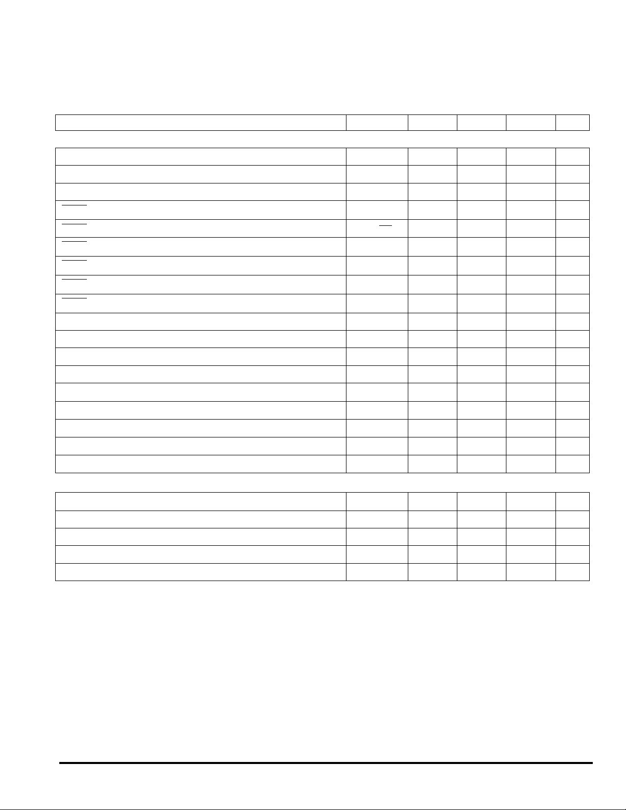
MAXIMUM RATINGS
All voltages are with respect to ground unless otherwise noted.
Rating Symbol Value Unit
Supply Voltage V
Switching Node SW -1.0 to 7.0 V
Buck Regulator Bootstrap Input (BOOT - SW) BOOT -0.3 to 8.5 V
Boost Regulator Output V
Boost Regulator Drain V
RESET Drain Voltage
Enable Pins (EN1, EN2)
Logic Pins (SDA, SCL, CLKSYN)
Analog Pins (INV, V
Analog Pins (LDRV
Analog Pins (CLKSEL, ADDR, RT, FREQ, V
ESD Voltage
Human Body Model (Note 1)
Machine Model (Note 2)
Storage Temperature T
Power Dissipation (T
Lead Soldering Temperature (Note 4) T
Maximum Junction Temperature T
Thermal Resistance, Junction to Ambient (Note 5) R
Thermal Resistance, Junction to Base (Note 6) R
OPERATING CONDITIONS
Supply Voltage (V
Operational Package Temperature (Ambient Temperature) T
Notes
1. ESD1 testing is performed in accordance with the Human Body Model (C
2. ESD2 testing is performed in accordance with the Machine Model (C
3. Maximum power dissipation at indicated junction temperature.
4. Lead soldering temperature limit is for 10 seconds maximum duration. Contact Motorola Sales Office for device immersion soldering time/
temperature limits.
5. Thermal resistance measured in accordance with EIA/JESD51-2.
6. Theoretical thermal resistance from the die junction to the exposed pins.
, RESET)
OUT
LFB, LDO, LCMP, CS)
,
= 85°C) (Note 3) P
A
, V
IN1
)V
IN2
DDI
, V
IN1
IN2
BST
BD
RESET
–
–
–
–
)
ZAP
–
V
ESD1
V
ESD2
STG
D
SOLDER
JMAX
JA
θ
JB
θ
, V
IN1
IN2
A
=100 pF, R
ZAP
=200 pF, R
ZAP
ZAP
=0 Ω).
=1500 Ω).
-0.3 to 7.0 V
-0.3 to 8.5 V
-0.3 to 9.5 V
-0.3 to 7.0 V
-0.3 to 7.0 V
-0.3 to 7.0 V
-0.3 to 7.0 V
-0.3 to 8.5 V
-0.3 to 3.6 V
±2000
±200
-65 to 150 °C
TBD W
260 °C
125 °C
68 °C/W
18 °C/W
2.8 to 6.0 V
-40 to 85 °C
V
MOTOROLA ANALOG INTEGRATED CIRCUIT DEVICE DATA 33702
For More Information On This Product,
Go to: www.freescale.com
5

Freescale Semiconductor, Inc.
STATIC ELECTRICAL CHARACTERISTICS
Characteristics noted under conditions -40°C ≤ T
J
application circuit (see Figure 20) unless otherwise noted.
Characteristic Symbol Min Typ Max Unit
GENERAL
Operating Voltage Range (V
Start-Up Voltage Threshold (Boost Switching)
Undervoltage Lockout
V
BST
Input DC Supply Current (Normal Operation Mode, Enabled)
Pin Input Supply Current (EN1 = EN2 = 0)
V
IN1
V
Pin Input Leakage Current (EN1 = EN2 = 0)
IN2
V
Internal Supply Voltage
DDI
nc...
V
Maximum Output Current
DDI
I
IN1
, V
IN2
)
BUCK CONVERTER
Buck Converter Output Voltage Range
I
= 30 mA to 3.0 A, V
VOUT
Buck Converter Feedback Voltage
= 30 mA to 3.0 A, V
I
VOUT
Includes Load Regulation Error
Buck Converter Voltage Margining Step
Buck Converter Line Regulation
V
= V
IN1
Buck Converter Load Regulation
I
VOUT
Input Leakage Current
V
OUT
V
OUT
cale Semiconductor,
High-Side Power MOSFET Q1 R
ID = 1.0 A, TA = 25°C, V
Low-Side Power MOSFET Q2 R
ID = 1.0 A, TA = 25°C, V
Frees
Buck Converter Peak Current Limit (High Level)
Buck Converter Valley Current Limit (Low Level)
V
Pull-Down MOSFET Q3 Current Limit
OUT
= 25°C, V
T
A
Pull-Down MOSFET Q3 R
V
OUT
= 1.0 A, TA = 25°C, V
I
D
Thermal Shutdown (Switcher, V
Thermal Shutdown Hysteresis
= 2.8 V to 6.0 V, I
IN2
= 30 mA to 3.0 A
= 5.0 V
= 8.0 V
BST
BST
BST
BST
IN1
IN1
= 8.0 V
= 8.0 V
= 8.0 V
OUT
= V
= 2.8 V to 6.0 V
IN2
= V
= 2.8 V to 6.0 V. No RB Resistor.
IN2
= 3.0 A
VOUT
DS(ON)
DS(ON)
DS(ON)
FET)
≤ 125°C unless otherwise noted. Input voltages V
V
IN
V
ST
V
BST_UVLO
I
IN
I
IN1
I
IN2
V
DDI
I
DDI
V
OUT
V
INV
V
MVO
REG
LNVO
REG
LDVO
I
VOUTLK
R
DS(ON)
R
DS(ON)
I
H_LIM
I
L_LIM
I
Q3_LIM
R
DS(ON)
T
SD
T
SDHys
2.8 – 6.0 V
–1.61.8V
–6.0–V
–60–mA
–9.0–mA
–TBD–µA
3.0 – 3.3 V
–TBD–µA
0.8 – 5.0
0.784 0.8 0.816
–1.0–%
-1.0 – 1.0
-1.0 – 1.0
–TBD–
––50
––50
3.4 4.5 6.0 A
1.7 2.25 3.0 A
–2.0–
––1.0
150 170 190 °C
–15–°C
IN1
= V
= 3.3 V using the typical
IN2
V
V
%
%
µA
mΩ
mΩ
A
Ω
33702 MOTOROLA ANALOG INTEGRATED CIRCUIT DEVICE DATA
6
For More Information On This Product,
Go to: www.freescale.com

nc...
I
cale Semiconductor,
Frees
Freescale Semiconductor, Inc.
STATIC ELECTRICAL CHARACTERISTICS (continued)
Characteristics noted under conditions -40°C ≤ T
application circuit (see Figure 20) unless otherwise noted.
Characteristic Symbol Min Typ Max Unit
ERROR AMPLIFIER (BUCK CONVERTER)
Input Impedance (Note 7)
Output Impedance (Note 7)
DC Open Loop Gain (Note 7)
Gain Bandwidth Product (Note 7)
Slew Rate (Note 7)
Output Voltage Swing – High Level
> 3.3 V, I
V
IN1
Output Voltage Swing – Low Level
I
= -1.0 mA (Note 7)
OEA
Slope Compensation Ramp (Note 7)
OSCILLATOR
Oscillator Low Level Output Voltage (Pin CLKSYN), CLKSEL Open
Oscillator High Level Output Voltage (Pin CLKSYN), CLKSEL Open
Oscillator Input Voltage Threshold (Pin CLKSYN), CLKSEL Grounded
Oscillator Frequency Adjusting Reference Voltage (FREQ)
Oscillator Frequency Adjusting Resistor Range
BOOST REGULATOR
Boost Regulator Output Voltage
I
= 20 mA, V
BST
Boost Regulator Start-Up Voltage
Boost Regulator Peak Current Limit (Power FET Peak Current)
Boost Regulator Power FET Valley Current Limit (Low Level)
Boost Power FET R
IBD = 1.0 A, TA = 25°C
Boost Regulator Recommended Output Capacitor
Boost Regulator Recommended Output Capacitor Maximum ESR
Notes
7. Design information only. It is not production tested.
= -1.0 mA (Note 7)
OEA
= V
IN1
DS(ON)
= 2.8 V to 6.0 V
IN2
≤ 125°C unless otherwise noted. Input voltages V
J
= V
IN1
R
IN
R
OUT
A
VOL
GBW – 35 – MHz
SR – 200 – V/µs
V
EA_OH
V
EA_OL
V
SCRamp
V
OSC_OL
V
OSC_OH
V
OSC_IH
V
FREQ
R
FREQ
V
BST
V
IN_BSU
I
P_BD
I
L_BD
R
DS(ON)
C
BST
ESR
CBST
– 500 – kΩ
– 150 – Ω
–80–dB
–2.0–
–0.4–
–0.6–V
––0.4V
3.0 – – V
1.2 1.6 2.0 V
–1.29–V
100 – 200 kΩ
7.5 8.0 8.5
–1.61.8V
0.75 1.0 1.5 A
450 600 800 mA
– 150 400
–10–µF
– 100 – mΩ
= 3.3 V using the typical
IN2
V
V
V
mΩ
MOTOROLA ANALOG INTEGRATED CIRCUIT DEVICE DATA 33702
For More Information On This Product,
Go to: www.freescale.com
7

Freescale Semiconductor, Inc.
STATIC ELECTRICAL CHARACTERISTICS (continued)
Characteristics noted under conditions -40°C
≤ TJ ≤ 125°C unless otherwise noted. Input voltages V
application circuit (see Figure 20) unless otherwise noted.
Characteristic Symbol Min Typ Max Unit
LINEAR REGULATOR (LDO)
LDO Output Voltage Range
V
= V
IN1
LDO Feedback Voltage, LFB Pin Connected to LDO Pin
V
IN1
Regulation Error
LDO Voltage Margining Step Size
LDO Line Regulation
V
IN1
LDO Load Regulation
nc...
I
I
LDO
LDO Ripple Rejection, Dropout Voltage V
Sinusoidal, f = 300 kHz, I
LDO Maximum Dropout Voltage (V
V
LDO
LDO Current Sense Comparator Threshold Voltage (V
LDO Pin Input Current
LDO Feedback Input Current (LFB Pin)
LDO Drive Output Current (LDRV
LDO Drive Current Limit (LDRV Pin)
CS Pin Input Leakage Current
V
CS
LDO Error Amplifier Input Impedance (LFB Pin)
= 2.8 V to 6.0 V, I
IN2
= V
= 2.8 V to 6.0 V, I
IN2
= V
= 2.8 V to 6.0 V, I
IN2
= 10 mA to 1000 mA
= 2.5 V, I
= 5.0 V
= 1000 mA
LDO
LDO
= 10 mA to 1000 mA
LDO
= 10 mA to 1000 mA. Includes Load
LDO
= 1000 mA
LDO
= 1.0 V, V
DO
= 500 mA
- V
LDO
)
Pin)
IN
cale Semiconductor,
LDO Error Amplifier Output Impedance (LCMP Pin)
LDO Pull-Down MOSFET Q4 Current Limit
T
= 25°C, V
A
Frees
LDO Pull-Down MOSFET Q4 R
ID = 1.0 A, TA = 25°C, V
LDO Recommended Output Capacitance
LDO Recommended Output Capacitor ESR
Thermal Shutdown (LDO Pull-Down FET Q4)
Thermal Shutdown Hysteresis
= 8.0 V (LDO Pin)
BST
BST
DS(ON)
= 8.0 V
RIPPLE
- V
CS
= +1.0 V p-p
)
LDO
V
REG
REG
V
I
R
ESR
T
V
LDO
V
LDO
MLDO
LNVLDO
LDVLDO
LDO_RR
V
DO
V
CSTH
I
LDO
I
LFB
I
LDRV
I
DRLIM
I
CSLK
R
IN
R
OUT
Q4_LIM
DS(ON)
C
LDO
CLDO
T
SD
SDHys
= V
IN1
0.8 – 5.0
0.784 0.8 0.816
–1.0–%
-1.0 – 1.0
-1.0 – 1.0
–40–
––TBD
35 45 55 mV
1.6 2.0 2.4 mA
-5.0 – 5.0 µA
2.0 3.6 5.0 mA
–3.6–mA
50 – 300
–TBD–Ω
–TBD–Ω
–-2.0–
––1.0
–10–µF
–TBD–mΩ
150 170 190 °C
–15–°C
= 3.3 V using the typical
IN2
V
V
%
%
dB
V
µA
A
Ω
33702 MOTOROLA ANALOG INTEGRATED CIRCUIT DEVICE DATA
8
For More Information On This Product,
Go to: www.freescale.com
nc...
I
cale Semiconductor,
Frees
Freescale Semiconductor, Inc.
STATIC ELECTRICAL CHARACTERISTICS (continued)
Characteristics noted under conditions -40°C ≤ T
application circuit (see Figure 20) unless otherwise noted.
Characteristic Symbol Min Typ Max Unit
CONTROL AND SUPERVISORY CIRCUITS
Enable (EN1, EN2) Input Voltage Threshold
Enable (EN1, EN2) Input Voltage Threshold Hysteresis
Enable (EN1, EN2) Pull-Down Resistance
RESET Low-Level Output Voltage, I
RESET Leakage Current, OFF State, Pulled Up to 5.0 V
RESET Undervoltage Threshold on V
RESET Overvoltage Threshold on V
RESET Undervoltage Threshold on V
RESET Overvoltage Threshold on V
Reset Timer Voltage Threshold
Reset Timer Source Current
Reset Timer Leakage Current
Reset Timer Saturation Voltage, Reset Timer Current = 300 µA
Maximum Value of the Reset Timer Capacitor
CLKSEL Threshold Voltage
CLKSEL Pull-Up Resistance
ADDR Threshold Voltage
ADDR Pull-Up Resistance
SDA, SCL Pins I2C Bus (STANDARD)
Input Threshold Voltage
Input Voltage Threshold Hysteresis
SDA, SCL Input Current, Input Voltage = 0.4 V to 6.0 V
SDA Low-Level Output Voltage, 3.0 mA Sink Current
SCA, SCL Capacitance
Notes
8. This parameter does not include the tolerance of the external resistor divider.
= 5.0 mA
OL
OUT
(∆V
OUT
LDO
(∆V
LDO
(∆V
(∆V
J
OUT/VOUT)
OUT/VOUT)
LDO/VLDO)
LDO/VLDO)
≤ 125°C unless otherwise noted. Input voltages V
(Note 8)
(Note 8)
(Note 8)
(Note 8)
V
TH_EN
V
IHYS
R
V
I
LKG-RST
V
OUTITh
V
OUTITh
V
LDOITh
V
LDOITh
V
TH-RT
I
S-RT
I
LKG-RT
V
SAT-RT
C
V
CLKS
th
R
PU-CLKS
V
ADDR
th
R
PU-ADDR
V
V
IHYS
V
C
PU
OL
Ith
I
OL
= V
IN1
1.2 1.6 2.0 V
–0.1–V
30 60 120 kΩ
––0.4V
––10µA
-10 -7.5 -5.0 %
5.0 7.5 10 %
-10 -7.5 -5.0 %
5.0 7.5 10 %
TBD 1.2 TBD V
20–30mA
-1.0 – 1.0 µA
– 100 TBD mV
t
I
I
––47µF
1.2 1.6 2.0 V
60 120 240 kΩ
1.2 1.6 2.0 V
60 120 240 kΩ
1.3 – 1.7 V
–0.2–V
––10µA
––0.4V
– – 10 pF
= 3.3 V using the typical
IN2
MOTOROLA ANALOG INTEGRATED CIRCUIT DEVICE DATA 33702
For More Information On This Product,
Go to: www.freescale.com
9

Freescale Semiconductor, Inc.
DYNAMIC ELECTRICAL CHARACTERISTICS
Characteristics noted under conditions -40°C
application circuit (see Figure 20) unless otherwise noted.
Characteristic Symbol Min Typ Max Unit
BUCK CONVERTER
Duty Cycle Range (Normal Operation) D 0 – 90 %
Switching Node SW Rise Time (Note 9)
I
= 3.0 A
LOAD
Switching Node SW Fall Time (Note 9)
I
= 3.0 A
LOAD
Maximum Deadtime (Note 9) t
Buck Control Loop Propagation Delay (Note 9)
V
< 0.8 V to VSW > 90% of High Level or V
INV
Low Level
nc...
Soft Start Duration (Power Sequencing Disabled, EN1 = 1, EN2 = 1) t
I
Fault Condition Timeout t
Retry Timer Cycle t
OSCILLATOR
Oscillator Default Frequency (Switching Frequency), FREQ Pin Open f
Oscillator Frequency Range f
Oscillator Frequency Accuracy
R
= 100 kΩ
F
Oscillator Frequency Accuracy
R
= 200 kΩ
F
Oscillator Output Signal Duty Cycle (Square Wave, 180° Out-of-Phase with the
Internal Suitable Oscillator)
Synchronization Pulse Minimum Duration t
BOOST REGULATOR
cale Semiconductor,
Boost Regulator FET Maximum ON Time t
Boost Regulator Control Loop Propagation Delay (Note 9) t
Boost Switching Node V
Frees
= 20 mA
I
BST
Boost Switching Node V
= 20 mA
I
BST
Notes
9. Design Information only. Not production tested.
Rise Time (Note 9)
BD
Fall Time (Note 9)
BD
≤ TJ ≤ 125°C unless otherwise noted. Input voltages V
t
RISE
–
t
FALL
–
–TBD–ns
–50–
200 350 800 µs
–10–ms
– 100 – ms
270 300 330 kHz
200 400 kHz
360 400 440
180 200 220
–50–
300 – – ns
–24–µs
–50–ns
–1540
–1540
> 0.8 V to VSW < 10% of
INV
D
t
PD
SS
FAULT
R
et
OSC
OSC
f
OSC
f
OSC
D
OSC
SYNC
ON
BST_PD
t
B_RISE
t
B_FALL
IN1
= V
= 3.3 V using the typical
IN2
TBD
TBD
–
–
ns
ns
ns
kHz
kHz
%
ns
ns
33702 MOTOROLA ANALOG INTEGRATED CIRCUIT DEVICE DATA
10
For More Information On This Product,
Go to: www.freescale.com

Freescale Semiconductor, Inc.
DYNAMIC ELECTRICAL CHARACTERISTICS (continued)
Characteristics noted under conditions -40°C
application circuit (see Figure 20) unless otherwise noted.
Characteristic Symbol Min Typ Max Unit
LINEAR REGULATOR (LDO)
LDO Output Current Slew Rate I
Fault Condition Timeout t
Retry Timer Cycle t
SCA, SCL PIN, I2C BUS (STANDARD)
SCL Clock Frequency
Bus Free Time Between a STOP and a START Condition
Hold Time (Repeated) START Condition (After this period, the first clock pulse
is generated.)
nc...
I
Low Period of the SCL Clock
High Period of the SCL Clock
SDA Fall Time from V
3.0 mA Sink Current
Setup Time for a Repeated START Condition
Data Hold Time for I
Data Setup Time
Setup Time for STOP Condition
Capacitive Load for Each Bus Line
Notes
10. Design Information only. Not production tested.
11. The device provides an internal hold time of at least 300 ns for the SDA signal (refer to the V
region of the falling edge of SCL.
2
to V
IH_MAX
C bus devices (Note 10), (Note 11)
, Bus Capacitance 10 pF to 400 pF,
IL_MIN
cale Semiconductor,
≤ TJ ≤ 125°C unless otherwise noted. Input voltages V
SR
FAULT
R
f
SCL
t
BUF
t
HD-STA
t
LOW
t
HIGH
t
F
t
SU-STA
t
HD-DAT
t
SU-DAT
t
SU-STO
C
et
B
– TBD – mA/µs
–1.0–ms
– 100 – ms
0 – 100 kHz
4.7 – – µs
4.0 – –
4.7 – – µs
4.0 – – µs
– – 250
4.7 – – µs
0––µs
250 – – ns
4.0 – – µs
– – 400 pF
of the SCL signal) to bridge the undefined
IH_MIN
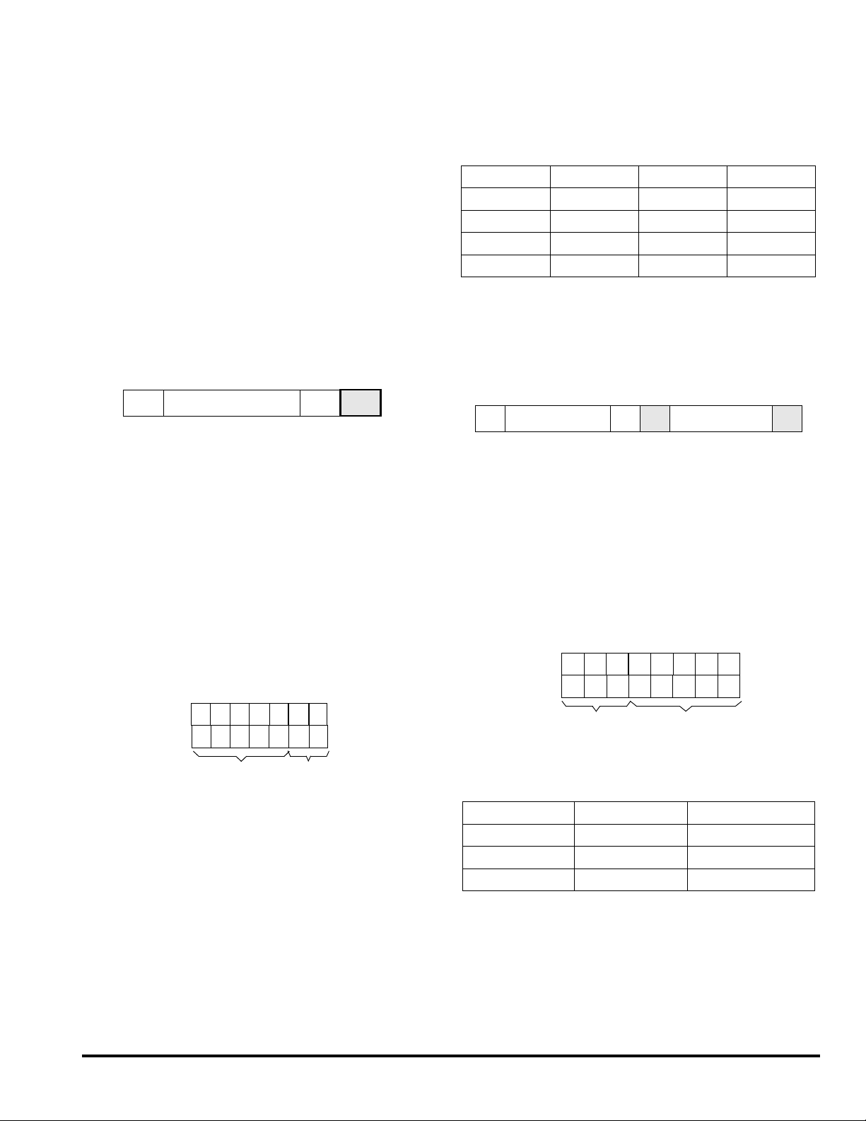
Timing Diagram
IN1
= V
= 3.3 V using the typical
IN2
µs
ns
Frees
t
HD-STA
t
HD-STA
MOTOROLA ANALOG INTEGRATED CIRCUIT DEVICE DATA 33702
t
HD-DAT
Figure 2. Definition of Time on the I2C Bus
For More Information On This Product,
t
SU-DAT
t
SU-STA
Go to: www.freescale.com
t
SU-STO
11

Freescale Semiconductor, Inc.
Electrical Performance Curves
nc...
I
Figure 3. Buck R
DS(ON)
(Temp)
Figure 6. I
LIM
(Temp)
cale Semiconductor,
Frees
Figure 4. F
OSC
(RF)
Figure 7. Vref (Temp)
Figure 5. Buck Efficiency
33702 MOTOROLA ANALOG INTEGRATED CIRCUIT DEVICE DATA
12
For More Information On This Product,
Go to: www.freescale.com
Figure 8. RT Timer (R
, Ct)
t

Freescale Semiconductor, Inc.
SYSTEM/APPLICATION INFORMATION
INTRODUCTION
nc...
I
cale Semiconductor,
Frees
The 33702 power supply integrated circuit provides the
means to efficiently supply the Power QUICC and other families
of Motorola microprocessors. It incorporates a highperformance synchronous buck regulator, supplying the
microprocessor’s core, and a low dropout (LDO) linear regulator
providing the microprocessor I/O and bus voltages.
FUNCTIONAL DESCRIPTION
Switching Regulator
The switching regulator is a high-frequency (300 kHz default,
adjustable in the range from 200 kHz to 400 kHz), synchronous
buck converter driving integrated high-side and low-side
N-channel power MOSFETs. The switching regulator output
voltage is adjustable by means of an external resistor divider to
provide the required output voltage within plus/ minus two
percent accuracy, and it is intended to directly power the core
of the microprocessor. The buck controller utilizes a Sensorless
PWM Current Mode Control topology to achieve excellent line
rejection, stabilize the feedback loop, and provide cycle-bycycle current limiting.
A typical bootstrap technique is used to provide voltage
necessary to properly enhance the high-side MOSFET gate.
When the regulator is supplied only from low-input voltage
(e.g., single +3.3 V supply rail), the bootstrap capacitor is
charged from the internal boost regulator output V
an external diode. This arrangement allows the 33702 to
operate from very low input voltage and also comply with the
power sequencing requirements of the supplied
microcontroller.
To avoid destruction of the supplied circuits, a current limit
with retry capability was implemented in the switching regulator.
When an overcurrent condition occurs and the switch current
reaches the peak current limit value, the main (high-side) switch
is turned off until the inductor current decays to the valley value,
which is one-half of the peak current limit. If an overcurrent
condition exists for 10 ms, the buck regulator control circuit
shuts the switcher OFF and the switcher retry timer starts to
time out. When the timer expires after 100 ms, the switcher
engages the start-up sequence and runs for 10 ms, repeatedly
checking for the overcurrent condition. During the current
limited operation (e.g., in case of short circuit on the switching
regulator output), the switching regulator operation is not
synchronized to the oscillator frequency.
The output voltage V
external resistor divider connected to the feedback control pin
INV. The switching regulator output voltage can be adjusted in
the range of 0.8 V to 5.0 V, but the V
always lower than the input voltage to the regulator. Power-up,
power-down, and fault management are coordinated with the
linear regulator.
can be adjusted by means of an
OUT
output voltage is
OUT
through
BST
This device incorporates many advanced features; e.g.,
precisely maintained up/down power sequencing, ensuring the
proper operation and protection of the CPU and power system.
At the same time, it provides high flexibility of configuration,
allowing the maximum optimization of the power supply system.
Thermal Shutdown
To increase the overall safety of the system designed with
the 33702, an internal thermal shutdown function has been
incorporated into the switching regulator circuit. The 33702
senses the temperature of the buck regulator main switching
FET (high-side FET Q1; see Figure 1), the low-side
(synchronous FET Q2), and control circuit. If the temperature of
any of the monitored components exceeds the limit of safe
operation (thermal shutdown), the switching regulator will be
shut down. After the temperature falls below the value given by
the thermal shutdown hysteresis window, the switcher will retry
to operate again.
The V
shutdown control. When the Q3 temperature exceeds the
thermal shutdown limit, the Q3 will be turned off without
affecting the switcher operation.
Soft Start
A switching regulator soft start feature is incorporated in the
33702. The soft start is active each time the IC is enabled, V
is reapplied, or after a fault retry. Other transient events do not
activate the soft start.
Boost Regulator
A boost regulator provides a high voltage necessary to
properly drive the buck regulator power MOSFETs, especially
during the low input voltage condition. The LDO regulator
external N-channel MOSFET gate is also powered from the
boost regulator. In order to properly enhance the high-side
MOSFETs when only a +3.3 V supply rail powers the integrated
circuit, the boost regulator provides an output voltage of 8.0 V
nominal value.
The 33702 boost regulator uses a simple hysteretic current
control technique, which allows fast power-up and does not
require any compensation. When the boost regulator main
power switch (low side) is turned on, the current in the inductor
starts to ramp up. After the inductor current reaches the upper
current limit (nominally set at 1.0 A), the low-side switch is
turned off and the current charges the output capacitor through
the internal rectifier. When the inductor current falls below the
valley current limit value (nominally 600 mA), the low-side
switch is turned on again, starting the next switching cycle. After
pull-down FET Q3 has an independent thermal
OUT
IN
MOTOROLA ANALOG INTEGRATED CIRCUIT DEVICE DATA 33702
For More Information On This Product,
Go to: www.freescale.com
13

Freescale Semiconductor, Inc.
the boost regulator output capacitor reaches its regulation limit,
the low-side switch is turned off until the output voltage falls
below the regulation limit again.
Oscillator
A 300 kHz (default) oscillator sets the switching frequency of
the buck regulator. The frequency of the oscillator can be
adjusted between 200 kHz and 400 kHz by an optional external
resistor R
circuit to ground. See Figure 4 for frequency resistor selection.
The CLKSYN pin can be configured either as an oscillator
output when the CLKSEL pin is left open or it can be used as a
synchronization input when the CLKSEL pin is grounded. The
oscillator output signal is a square wave logic signal with
50 percent duty cycle, 180 degrees out-of-phase with the
internal clock signal. This allows opposite phase
synchronization of two 3370x devices.
nc...
When the CLKSYN pin is used as synchronization input
I
(CLKSEL pin grounded), the external resistor R
the chart in Figure 4 should be used to synchronize the internal
slope compensation ramp to the external clock. Operation is
only recommended between 200 kHz and 400 kHz. The
supplied synchronization signal does not need to be 50 percent
duty cycle. Minimum pulse width is 300 ns.
connected from the FREQ pin of the integrated
F
chosen from
F
Low Dropout Linear Regulator (LDO)
The adjustable low dropout linear regulator (LDO) is capable
of supplying a 1.0 A output current. It has a current limit with
retry capability. When the voltage measured across the current
sense resistor reaches the 45 mV threshold, the control circuit
limits the current for 1.0 ms and if the overcurrent condition still
exists the linear regulator is turned off. At the same time the
overcurrent condition is detected, the Retry Timer starts to time
out. When the timer expires after 100 ms, the LDO tries to
power up again for 1.0 ms, repeatedly checking for the
overcurrent condition. The current limit of the LDO can be set
cale Semiconductor,
by using the following formula:
I
= 45 mV/R
LIM
Where RS is the LDO current sense resistor, connected
between the CS pin and the LDO pin output (see Figure 20).
Frees
When no current sense resistor is used, it is still possible to
detect the overcurrent condition by tying the current sense pin
CS to the V
is sensed by saturation of the linear regulator driver buffer.
The output voltage of the LDO can be adjusted by means of
an external resistor divider connected to the feedback control
pin LFB. The linear regulator output voltage can be adjusted in
the range of 0.8 V to 5.0 V, but the LDO output voltage is always
lower than the input voltage to the regulator. Power-up, powerdown, and fault management are coordinated with the
switching regulator.
Thermal Shutdown
The LDO pull-down FET Q4 has an independent thermal
shutdown control. When the Q4 temperature exceeds the
voltage. In this case, the overcurrent condition
BST
S
thermal shutdown limit, the Q4 will be turned off without
affecting the LDO operation.
Voltage Margining
The 33702 includes a voltage margining feature accessed
through the I
adjustment of the Switcher V
V
LDO
range of ±7%. This feature allows for worst case system
validation; i.e., determining the design margin. Margining
details are described in the section entitled I
beginning on page 19 of this datasheet.
RESET
The RESET pin is an open drain output. The Reset Control
circuit supervises both output voltages—the linear regulator
output V
either of these two regulators is out of regulation (high or low),
RESET pin is pulled low. There is a 20 µs delay filter
the
preventing erroneous resets. During power-up sequencing,
RESET is held low until the Reset Timer times out.
2
C bus. Voltage margining allows for independent
voltage and the linear output
OUT
. Each can be adjusted up and down in 1% steps to a
2
C Bus Operation,
and the switching regulator output V
LDO
OUT
. When
Reset Timer Power-Up Delay (RT)
The Reset Timer Power-Up Delay (RT) pin is used to set the
delay between the time when the LDO and switcher outputs are
active and stable and the release of the
external resistor and capacitor are used to program the timer.
The power-up delay can be obtained by using the following
formula:
T
= 10 ms + RtC
D
Where Rt is the Reset Timer programming resistor and Ct is the
Reset Timer programming capacitor, both connected in parallel
from RT to ground.
Note Observe the maximum Ct value and expect reduced
accuracy if R
is less than 10 kΩ.
t
RESET output. An
t
Watchdog Timer
A watchdog function is available via I2C bus communication.
It is possible to select either window watchdog or time-out
watchdog operation, as illustrated in Figure 9 on page 15.
Watchdog time-out starts when the watchdog function is
activated via I2C bus sending a Watchdog Programming
command byte, thus determining watchdog operation (window
or time-out) and period duration (refer to Table 1, page 15). If
the watchdog is cleared by receiving a new Watchdog
Programming command through the I
timer is reset and the new time-out period begins. If the
watchdog time expires, the
for a time determined by the RC components of the RT timer
plus 10 ms. After a watchdog time-out, the function is no longer
active.
RESET will become active (LOW)
2
C bus, the watchdog
33702 MOTOROLA ANALOG INTEGRATED CIRCUIT DEVICE DATA
14
For More Information On This Product,
Go to: www.freescale.com

V
Freescale Semiconductor, Inc.
nc...
I
cale Semiconductor,
Frees
Watchdog Closed
No Watchdog Clear Allowed
50% of Watchdog Period
Timing Selected via 1
Timing Selected via I
Figure 9. Watchdog Operation
Table 1. Watchdog Programming Command Byte
Address Value Action
01100000 1st Command
01100000 WD OFF
0 1 1 0 1 0 0 0 WD 1280 ms
0 1 1 0 1 0 0 1 WD 320 ms
01101010 WD 80 ms
01101011 WD 20 ms
0 1 1 0 1 1 0 0 WD 1280 ms
0 1 1 0 1 1 0 1 WD 320 ms
01101110 WD 80 ms
01101111 WD 20 ms
Notes
12.
The Watchdog feature will be turned
ON automatically after receiving any
other valid command byte changing
watchdog time.
When the Window Watchdog function is selected, the timer
cannot be cleared during the Closed Window time, which is
50% of the total watchdog period. When the watchdog is
cleared, the timer is reset and starts a new time-out period. If
the watchdog is not cleared during the Open Window time, the
RESET will become active (LOW) for a time determined by the
RC components of the RT timer plus 10 ms.
Watchdog Period
Window Watchdog
Window Open for Watchdog Clear
Watchdog Period
Time-Out Watchdog
(as a 2nd Command Byte)
Window Open
for Watchdog Clear
2
C Bus – See Table 1
2
C Bus – See Table 1
(Note 12)
WinOFF
WinOFF
WinOFF
WinOFF
WinON
WinON
WinON
WinON
EN1 and EN2 Control Pins
These two pins permit positive logic control of the Enable
function and selection of the Power Sequencing mode
concurrently. Table 2 depicts the EN1 and EN2 function and
Power Sequencing mode selection.
Both EN1 and EN2 pins have internal pull-down resistors
and both can withstand a short circuit to the supply voltage,
6.0 V.
Table 2. Operating Mode Selection
EN1 EN2 Operating Mode
0 0 Regulators Disabled
0 1 Standard Power Sequencing
1 0 Inverted Power Sequencing
1 1 Regulators Enabled,
No Power Sequencing
Power Sequencing Modes
The power sequencing of the two outputs of this power
supply IC is in compliance with the Motorola Power QUICC and
other 32-bit microprocessor requirements. When the input
voltage is applied, the switcher and linear regulator outputs
follow the supply rail voltage during power-up and power-down
in the limits given by the microcontroller power sequencing
specification, illustrated in Figures 10 through 12. There are two
possible power sequencing modes, Standard and Inverted, as
explained in more detail below. The third mode of operation is
Power Sequencing Disabled.
3.3 V Input Supply (I/O Voltage)
V Start-Up
Slope
1.0 V/ms
(typ.)
Figure 10. Standard Power Up / Down Sequence
∆V = 2.0 V
Max. Lead
V Start-Up
Figure 11. Standard Power Up / Down Sequence
1.8 V Core Voltage
∆V = 2.0 V
Max. Lead
in +3.3 V Supply System
5.0 V Input Supply
3.3 V I/O Voltage (V
1.8 V Core Voltage (V
∆V = 0.4 V
Max. Lag
in +5.0 V Supply System
LDO
)
∆V = 0.4 V
Max. Lag
∆V = 0.4 V
Max. Lag
)
OUT
∆V = 2.0
Max. Lead
∆V = 2.0 V
Max. Lead
MOTOROLA ANALOG INTEGRATED CIRCUIT DEVICE DATA 33702
For More Information On This Product,
Go to: www.freescale.com
15

Freescale Semiconductor, Inc.
∆V = 2.0 V
Max. Lead
V Start-Up
Figure 12. Inverted Power Up/ Down Sequence in +5.0 V
5.0 V Input Supply
3.3 V I/O Voltage (V
1.8 V Core Voltage
∆V = 0.4 V
Max. Lag
Supply System
OUT
(V
)
)
LDO
∆V = 0.4 V
Max. Lag
∆V = 2.0 V
Max. Lead
33702 POWER SEQUENCING
Standard Power Sequencing
When the power supply IC operates in the Standard Power
Sequencing mode, the switcher output provides the core
voltage for the microprocessor. This situation and operating
conditions are illustrated in Figure 10 and Figure 11. Table 2,
page 15, shows the Power Sequencing mode selection.
Inverted Power Sequencing
When the power supply IC is operating in the Inverted Power
Sequencing mode, the linear regulator (LDO) output provides
the core voltage for the microprocessor, as illustrated in
Figure 12. Table 2 shows the Power Sequencing mode
selection.
Requirements
nc...
I
1. I/O supply voltage not to exceed core voltage by more than
2.0 V.
2. Core supply voltage not to exceed I/O voltage by more
than 0.4 V.
Methods of Control
The 33702 has several methods of monitoring and
controlling the regulator output voltages, as described in the
paragraphs below. Power sequencing control is also achieved
through the intrinsic operation of the regulators. The EN1 and
EN2 pins can be used to disable the power sequencing (refer to
Table 2, page 15.
Intrinsic Operation
For both the LDO and switcher, whenever the output voltage
is below the regulation point, the LDO external Pass FET will be
on or the Buck High-Side FET will be on at a duty cycle
cale Semiconductor,
controlled by the switcher. Because these devices are FETs,
current can flow in either direction, balancing the voltages via
the common supply pin. The ability to maintain the FETs on will
depend on the available gate voltage, and thus the size of the
boost regulator storage capacitor.
Frees
Standard Power Sequencing Control
Comparators monitor voltage differences between the LDO
(LDO pin) and the switcher (V
1. LDO > V
forced off. This occurs whenever the LDO output voltage
exceeds the switcher output voltage by more than 1.8 V.
2. LDO > V
the LDO is insufficient and the LDO output voltage
exceeds the switcher output voltage by more than 1.9 V,
a 1.0 Ω shunt FET is turned on that discharges the LDO
load capacitor to ground. The shunt FET is used for
switcher output shorts to ground and for power down in
case of V
than the LDO.
3. LDO < V
LDO. Normal operation resumes when the LDO output
voltage is less than 1.7 V above the switcher output
voltage.
4. LDO < V
be forced off. This occurs whenever the LDO is less than
V
OUT
5. LDO < V
V
OUT
the Sync FET is forced on. This occurs when the switcher
output voltage exceeds the LDO output by more than
300 mV.
6. LDO > V
resumes when LDO > V
+ 1.8 V, turn off LDO. The LDO can be
OUT
+ 1.9 V, shunt LDO to ground. If turning off
OUT
≠ V
IN1
OUT
OUT
- 0.2 V.
OUT
sink FET. The Buck High-Side FET is forced off and
OUT
with the switcher output falling faster
IN2
+ 1.7 V, cancel (1) and (2) above, re-enable
- 0.2 V, turn off switcher. The switcher can
- 0.3 V, turn on Sync (LS) FET and 1.0Ω
, reset (4) and (5) above. Normal operation
pin) outputs as follows:
OUT
.
OUT
33702 MOTOROLA ANALOG INTEGRATED CIRCUIT DEVICE DATA
16
For More Information On This Product,
Go to: www.freescale.com

Freescale Semiconductor, Inc.
nc...
I
cale Semiconductor,
Frees
Inverted Power Sequencing Control
Comparators monitor voltage differences between the
switcher (V
1. V
OUT
can be forced off. This occurs whenever the V
voltage exceeds the LDO output voltage by more than
1.8 V.
2. V
OUT
the switcher V
voltage exceeds the LDO output voltage by more than
1.9 V, a 1.0 Ω shunt FET is turned on that discharges the
V
OUT
LDO output shorts to ground and for power-down in case
of V
V
OUT
3. V
OUT
V
OUT
voltage is less than 1.7 V above the LDO output voltage.
4. V
OUT
forced off. This occurs whenever the V
V
LDO
5. V
OUT
This occurs when the LDO output voltage exceeds the
V
OUT
6. V
OUT
resumes when V
pin) and LDO (LDO pin) outputs as follows:
OUT
> LDO + 1.8 V, turn off V
> LDO + 1.9 V, shunt V
is insufficient and the V
OUT
load capacitor to ground. The shunt FET is used for
≠ V
IN1
.
< LDO + 1.7 V, cancel (1) and (2) above, re-enable
. Normal operation resumes when the V
< LDO - 0.2 V, turn off LDO. The LDO can be
- 0.2 V.
< LDO - 0.3 V, turn on the 1.0Ω LDO sink FET.
output by more than 300 mV.
> LDO, reset (4) and (5) above. Normal operation
with LDO output falling faster than the
IN2
> LDO.
OUT
. The switcher V
OUT
OUT
to ground. If turning off
OUT
output
OUT
OUT
is less than
OUT
OUT
output
output
Standard Operating Mode
1. Single 3.3 V Supply, VIN = V
The 3.3 V supplies the microprocessor I/O voltage, the
switcher supplies core voltage (e.g., 1.8 V nominal), and the
LDO operates independently (see Figure 10, page 15). Power
sequencing depends only on the normal switcher intrinsic
operation to control the Buck High-Side FET.
Power Up
When V
point and the Buck High-Side FET will be on. In order not to
exceed the 2.0 V differential requirement between the I/O (V
and the core (V
and be able to maintain the 2.0 V or less differential. The
maximum slew rate for VIN is 1.0 V/ms.
Power Down
When V
therefore the Buck High-Side FET will be on. In the case where
V
OUT
attempt to maintain V
is rising, initially V
IN
), the switcher must start up at 2.0 V or less
OUT
is falling, V
IN
is falling faster than VIN, the Buck High-Side FET will
OUT
. In the case where VIN is falling faster
OUT
= V
IN1
will be below the regulation
OUT
will be below the regulation point;
= 3.3 V
IN2
IN
than V
load capacitor will be discharged through the Buck High-Side
FET to V
voltage (V
than a maximum of 0.4 V.
Shorted Load
1. V
2. V
3. V
2. Single 5.0 V Supply, V
V
switcher supplies the core (e.g., 1.8 V nominal) (see Figure 11,
page 15).
Power Up
current and capacitance, and the relative rise times of the V
and V
1. LDO rises faster than V
2. V
Power Down
capacitance and the relative fall times of the V
supplies. There are 2 cases:
)
1. V
2. LDO falls faster than V
, the Buck High-Side FET is also on, and the V
OUT
. Thus, provided VIN does not fall too fast, the core
IN
) will not exceed the I/O voltage (VIN) by more
OUT
shorted to ground. This will cause the I/O voltage to
OUT
exceed the core voltage by more than 2.0 V. No load
protection.
shorted to ground. Until the switcher load
IN
capacitance is discharged, the core voltage will exceed
the I/O voltage by more than 0.4 V. By the intrinsic
operation of the switcher, the load capacitor will be
discharged rapidly through the Buck High-Side FET to
.
V
IN
shorted to supply. No load protection. 33702
OUT
protected by current limit and thermal limit.
= V
IN1
IN2
The LDO supplies the microprocessor I/O voltage. The
This condition depends upon the regulator current limit, load
supplies. There are 2 cases:
IN2
OUT
methods (1) and (2) described in the Methods of Control
section, page 16.
rises faster than LDO. The switcher uses control
OUT
methods (4) and (5) described in the Methods of Control
section, page 16.
This condition depends upon the regulator load current and
falls faster than LDO. The LDO uses control
OUT
methods (1) and (2) described in the Methods of Control
section, page 16.
= V
In the case V
both the Buck High-Side FET and the LDO external Pass
FET, and will discharge the LDO load capacitor into the V
supply.
methods (4) and (5) described in the Methods of Control
section, page 16.
IN1
, the intrinsic operation will turn on
IN2
OUT
, or Dual Supply V
IN2
. The LDO uses control
. The switcher uses control
IN1
and V
IN1
IN2
OUT
≠
IN1
IN
MOTOROLA ANALOG INTEGRATED CIRCUIT DEVICE DATA 33702
For More Information On This Product,
Go to: www.freescale.com
17

Freescale Semiconductor, Inc.
Shorted Load
1. V
2. LDO shorted to ground. The switcher uses control
3. V
4. V
5. V
6. LDO shorted to supply. No load protection. 33702
shorted to ground. The LDO uses method (1) and
OUT
(2) described in the Methods of Control section, page 16.
methods (4) and (5) described in the Methods of Control
section, page 16.
shorted to ground. This is equivalent to the LDO
IN1
output shorted to ground.
shorted to ground. This is equivalent to the switcher
IN2
output shorted to ground.
shorted to supply. No load protection. 33702
OUT
protected by current limit and thermal limit.
protected by current limit and thermal limit.
Inverted Operating Mode
nc...
1. Single 3.3 V Supply, VIN = V
I
The 3.3 V supplies the microprocessor I/O voltage, the LDO
supplies core voltage (e.g., 1.8 V nominal), and the switcher
V
operates independently. Power sequencing depends only
OUT
on the normal LDO intrinsic operation to control the Pass FET.
Power Up
When VIN is rising, initially LDO will be below the regulation
point and the Pass FET will be on. In order not to exceed the
2.0 V differential requirement between the I/O (VIN) and the
core (LDO), the LDO must start up at 2.0 V or less and be able
to maintain the 2.0 V or less differential. The maximum slew
rate for V
Power Down
When V
therefore the Pass FET will be on. In the case where LDO is
cale Semiconductor,
falling faster than V
LDO. In the case where VIN is falling faster than LDO, the Pass
FET is also on, and the LDO load capacitor will be discharged
through the Pass FET to VIN. Thus, provided VIN does not fall
Frees
too fast, the core voltage (LDO) will not exceed the I/O voltage
(V
IN
Shorted Load
1. LDO shorted to ground. This will cause the I/O voltage to
2. V
is 1.0 V/ms.
IN
is falling, LDO will be below the regulation point;
IN
, the Pass FET will attempt to maintain
IN
) by more than maximum of 0.4 V.
exceed the core voltage by more than 2.0 V. No load
protection.
shorted to ground. Until the LDO load capacitance is
IN
discharged, the core voltage will exceed the I/O voltage
by more than 0.4 V. By the intrinsic operation of the LDO,
IN1
= V
= 3.3 V
IN2
the load capacitor will be discharged rapidly through the
Pass FET to V
3. LDO shorted to supply. No load protection.
2. Single 5.0 V Supply, V
V
IN2
The switcher V
The LDO supplies the core (e.g., 1.8 V nominal) (see Figure 12,
page 16).
Power Up
This condition depends upon the regulator current limit, load
current and capacitance, and the relative rise times of the V
and V
Power Down
capacitance and the relative fall times of the V
supplies. There are 2 cases:
Shorted Load
supplies. There are 2 cases:
IN2
1. V
2. LDO rises faster than V
This condition depends upon the regulator load current and
1. LDO falls faster than V
In the case V
the Buck High-Side FET and the LDO external Pass FET,
and will discharge the V
supply.
2. V
1. LDO shorted to ground. The V
2. V
3. V
4. V
5. LDO shorted to supply. No load protection.
6. V
rises faster than LDO. The switcher V
OUT
control methods (4) and (5) described in the Methods of
Control section, page 17.
methods (1) and (2) described in the Methods of Control
section, page 17.
methods (4) and (5) described in the Methods of Control
section, page 17.
falls faster than LDO. The LDO uses control
OUT
methods (1) and (2) described in the Methods of Control
section, page 17.
(5) described in the Methods of Control section, page 17.
shorted to ground. The LDO uses control methods
OUT
(1) and (2) described in the Methods of Control section.
shorted to ground. This is equivalent to the LDO
IN1
output shorted to ground.
shorted to ground. This is equivalent to the switcher
IN2
output shorted to ground.
V
OUT
shorted to supply. No load protection. 33702
OUT
protected by current limit and thermal limit.
.
IN
= V
IN1
supplies the microprocessor I/O voltage.
OUT
OUT
= V
IN1
the intrinsic operation will turn both
IN2
OUT
, or Dual Supply V
IN2
OUT
. The LDO uses control
OUT
and V
IN1
. The V
load capacitor into the VIN
OUT
uses control
OUT
uses methods (4) and
IN1
uses
IN2
≠
IN1
33702 MOTOROLA ANALOG INTEGRATED CIRCUIT DEVICE DATA
18
For More Information On This Product,
Go to: www.freescale.com
Freescale Semiconductor, Inc.
I2C BUS OPERATION
nc...
I
cale Semiconductor,
Frees
Introduction
The 33702 device is compatible with the I2C interface
standard. SDA and SCL pins are the Serial Data and Serial
Clock pins of the I
I2C Command and Data Formats
Communication Start
Communication starts with a START condition, followed by
the slave device unique address. Figure 13 illustrates the data
transfer beginning an I
address.
Figure 13. Communication Using 7-Bit Address
Slave Address Definition
33702 has the two LSB’s address bits defined by the state of
the CLKSEL pin and the ADDR pin.
Note The state of the CLKSEL pin also defines the
configuration of the oscillator synchronization CLKSYN pin.
This feature allows up to four 33702 ICs to communicate in
the same I
address bits. A different combination of bits A1 and A0 is
assigned to each individual part to assure its unique address.
Figure 14 illustrates the flexible addressing feature for a 7-bit
address. Table 3 provides the definition of the selectable
portion of the device address.
Figure 14. Address Bit Definition for 7-Bit Address
2
C bus.
2
C communication for a 7-bit slave
S 7-Bit Address R/W
2
C bus, all of them sharing the same high-order
102
Bits
11101A1A0
3456
Fixed Address Selectable
Address
Ack
Table 3. Definition of Selectable Portion of Device Address
CLKSEL Pin ADDR Pin A1 A0
Low Low 0 0
Low Open 0 1
Open Low 1 0
Open Open 1 1
Writing Data Into the Slave Device
After the address acknowledgment by the slave, DATA can
be written into the slave registers. The R/W bit must be set to 0
so DATA will be read. Figure 15 shows the data write
sequence. Actions performed by the slave device are grayed.
S 7-Bit Address 0Ack DATA Ack
Figure 15. Data Transfer for Write Operations
Data Definition
For the sake of 33702 acting as a slave device, the master
writes a Command Byte and writes one Data Byte. The
Command Byte identifies the kind of operation required by the
master and has two fields, as illustrated in Figure 16:
1. Address field
2. Value field
The address field is selected from the list in Table 4.
Bits
7
6
D6
D7
Address Field Value Field
Figure 16. Command Byte
Table 4. Address Field Definitions
Code Operation Write
001 Voltage Margining W
010 Not Used –
011 Watchdog W
D5
321045
D4 D3 D1 D0
D2
Refer to Table 5, page 20, which summarizes the value field
definitions for the entire set of operation options.
MOTOROLA ANALOG INTEGRATED CIRCUIT DEVICE DATA 33702
For More Information On This Product,
Go to: www.freescale.com
19
Freescale Semiconductor, Inc.
Table 5. Command Byte Definitions
Operation Address Value Action
Voltage Margining
(As a 2nd
Command Byte)
LDO Output: x=0 0 0 1 x 0 1 0 1 + 5%
Switcher Output x=1 001x0110 + 6%
nc...
I
Watchdog
Programming
(As a 2nd
Command Byte)
cale Semiconductor,
Frees
Notes
13.
The Watchdog feature will be turned ON automatically
after receiving any other valid command byte changing
watchdog time.
001000001st Command
001x0000Output Normal
001x0001 + 1%
001x0010 + 2%
001x0011 + 3%
001x0100 + 4%
001x0111 + 7%
001x1001 - 1%
001x1010 - 2%
001x1011 - 3%
001x1100 - 4%
001x1101 - 5%
001x1110 - 6%
001x1111 - 7%
011000001st Command
01100000 WD OFF
(Note 13)
0 1 1 0 1 0 0 0 WD 1280 ms
0 1 1 0 1 0 0 1 WD 320 ms
01101010 WD 80 ms
01101011 WD 20 ms
0 1 1 0 1 1 0 0 WD 1280 ms
0 1 1 0 1 1 0 1 WD 320 ms
01101110 WD 80 ms
01101111 WD 20 ms
WinOFF
WinOFF
WinOFF
WinOFF
WinON
WinON
WinON
WinON
Security in Writing Commands
All writing operations are critical and must not be
inadvertently latched after a false command. To improve the
security level, a so-called first command is defined to initiate
each write communications.
A first command has the Command Byte address field equal
to the related operation one, followed by a null value field (all
zeros). Table 6 summarizes first command definitions. The
master sends the first command before the Command Byte for
the intended operation.
Table 6. First Command Definitions
First Command Operation
001 00000 Voltage Margining
011 00000 Watchdog Programming
Voltage Margining Operation
After starting the communication in Writing mode, the master
sends the first command followed by the specific Command
Byte to set the required voltage margining for either the LDO or
the switcher (see Figure 17). To achieve a simultaneous set for
both LDO and switcher, two specific commands must be issued
in sequence after the first command, one for each supply.
00 000001001 xxxxx
First Byte for Voltage Margining
Figure 17. Voltage Margining Programming
Note x bits are defined in Table 5.
Ack
Command Byte
(One Supply Only)
Watchdog Programming Operation
For watchdog operation control, the master periodically
sends a watchdog first command followed by a command byte
selecting, or confirming, the watchdog period according to the
options listed in Table 5. Also see Figure 18.
The internal watchdog timer will be cleared each time a
watchdog command is written into the device, provided it
arrives during the window open time. The Command 01100000
sent twice will shut the time OFF, and the watchdog function will
be disabled. Any other valid watchdog command turns on the
timer again.
01 000001101 xxxxx
First Byte for Watchdog Programming
Ack
Command Byte
Figure 18. Watchdog Timer Programming
Note x bits are defined in Table 5.
33702 MOTOROLA ANALOG INTEGRATED CIRCUIT DEVICE DATA
20
For More Information On This Product,
Go to: www.freescale.com

Freescale Semiconductor, Inc.
Communication Stop
Only the master can terminate the data transfer by issuing a
STOP condition. The slave waits for this condition to resume its
initial state waiting for the next START condition (see
Figure 19).
Data Transfer Example
The master device controlling the I2C bus will always start
addressing a 33702 slave IC in writing mode (R/W = 0) in order
to be able to write a Command Byte just after the address
acknowledge. I
master-transmitter and slave-receiver configuration.
Eventually this Command Byte can again define a Write
operation (e.g., Voltage Margining, see Figure 19), and the
master will keep the data transfer direction.
Figure 19 illustrates a communication beginning with the
nc...
I
slave address, the first command for voltage margining, and a
third byte containing the address field 001 and the value field
00101 corresponding with the LDO fifth setting (LDO output
voltage = +5% above its nominal value). If a simultaneous
2
C bus protocol defines this circumstance as a
setting for switcher is needed, a fourth byte should be included
before the STOP condition (P); for instance, 001 10010 to set
switcher in its second setting (switcher output voltage = +2%
above its nominal value).
S
A5
START
Slave Address
First Command for Voltage Margining
Figure 19. Complete Data Transfer Example
A2 A1
A3
001000Ack00
Address Field Value Field = LDO
0
Write
1
AckA6 A4 A0
00
th
Setting
5
10
1
Ack00
P
STOP
cale Semiconductor,
Frees
MOTOROLA ANALOG INTEGRATED CIRCUIT DEVICE DATA 33702
For More Information On This Product,
Go to: www.freescale.com
21
nc...
I
cale Semiconductor,
Frees
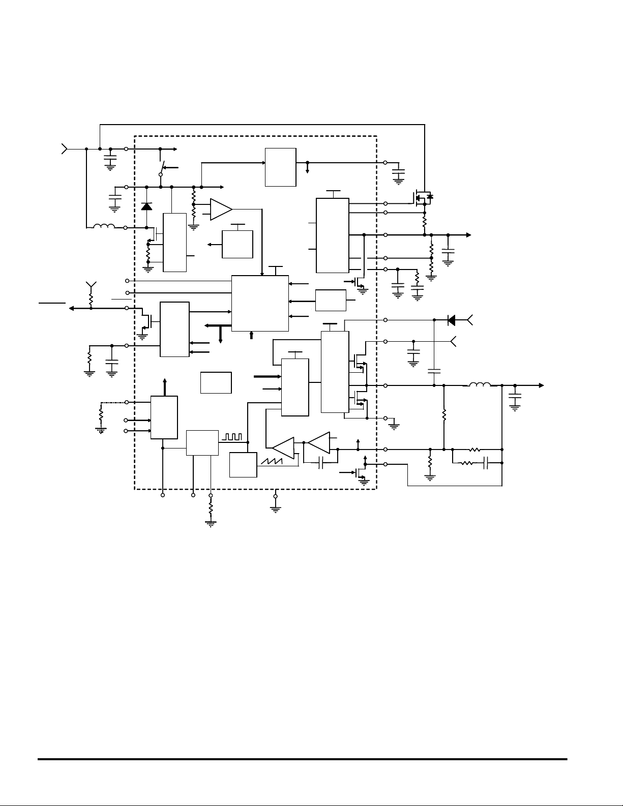
+3.3 V
+3.3V
+3.3V
Supply
Supply
Supply
Voltage
Voltage
Voltage
Reset
Reset
RESET
to MCU
to MCU
to MCU
10uF
10uF
10 µF
10uF
10uF
10 µF
+3.3V
+3.3V
+3.3 V or
or
or
V
V
V
V
LDO
LDO
LDO
LDO
5.1k
5.1k
R
Rt
Rt
t
100k
100k
R
R
pd
pd
10k
10k
C
C
IN
IN
C
C
BST
BST
10 µH
10uH
10uH
L
L
BST
BST
C
t
Ct
Ct
V
IN1
VIN1
VIN1
V
BST
VBST
VBST
V
VBD
VBD
BD
EN1
EN1
EN2
EN2
RESET
RESET
RT
RT
100nF
100nF
ADDR
ADDR
SDA
SDA
SCL
SCL
Freescale Semiconductor, Inc.
APPLICATION INFORMATION
V
VIN
VIN
IN
8.0V
8.0V
Interface
Interface
CLKSEL
CLKSEL
Control
Control
Control
Reset
Reset
Control
Control
I2C
I2C
I2C
Control
Control
I2C
I2C
I2C
Boost
Boost
Boost
POR
POR
Timer
Timer
Switcher
Switcher
Oscillator
Oscillator
300kHz
300kHz
CLKSYN
CLKSYN
Vref
Vref
Vref
Vref
Vref
Vref
SysCon
SysCon
INV
INV
LFB
LFB
Thermal
Thermal
-
-
+
+-+
Reference
Reference
Reset
Reset
Limit
Limit
FREQ
FREQ
R
R
F
F
(Optional)
(Optional)
VBST
VBST
V
BST
Power
Power
Enable
Enable
V
DDI
VDDI
VDDI
Bandgap
Bandgap
Voltage
Voltage
Voltage Margining
Voltage Margining
W-dog Timer
W-dog Timer
Watchdog Timer
Control
Control
Slope
Slope
Slope
Comp.
Comp.
Comp.
Figure 20. Simplified Block Diagram and Typical Application
Power
Power
Sequencing
Sequencing
I2C
I2C
I2C
SysCon
SysCon
SoftSt
SoftSt
V
VDDI
VDDI
DDI
Internal
Internal
Supply
Supply
V
DDI
VDDI
VDDI
PWM
PWM
Comp.
Comp.
(4)
(4)
GND
GND
Vref
Vref
V
VLDO
VLDO
Power
Power
Down
Down
V
VOUT
VOUT
Current
Current
V
DDI
VDDI
VDDI
Buck
Buck
Buck
Control
Control
Control
Logic
Logic
Logic
+
+-+
-
-
VDDI
VDDI
V
V
DDI
VDDI
VDDI
LDO
OUT
Limit
Limit
Error
Error
Amp.
Amp.
DDI
V
VBST
VBST
BST
Linear
Linear
Linear
Regulator
Regulator
Regulator
Control
Control
Control
I
I-lim
I-lim
I-lim
LIM
Pow. Seq.
Pow. Seq.
PWR Seq.
UVLO
UVLO
V
BST
VBST
VBST
Buck
Buck
Buck
HS
HS
HS
&
&
&
LS
LS
LS
Driver
Driver
Driver
0.8V
0.8V
+
+-+
-
-
Pow.
Pow.
PWR Seq.
Seq.
Seq.
V
VBST
VBST
To Reset
To Reset
Control
Control
V
VOUT
VOUT
OUT
Q4
Q4
BST
Q3
Q3
Q1
Q1
Q2
Q2
V
DDI
VDDI
VDDI
LDRV
LDRV
CS
CS
LDO
LDO
LFB
LFB
LCMP
LCMP
100pF
100pF
BOOT
BOOT
V
IN2
VIN2
VIN2
(2)
(2)
2 x 10 uF
2 x 10 uF
2 x 10 µF
SW
SW
(2)
(2)
PGND
PGND
(2)
(2)
INV
INV
V
VOUT
VOUT
OUT
C
C
1.0 uF
1.0 uF
1.5k
1.5k
IN
IN
?k
?k
?k
?k
?k
?k
R
R
0.068 R
0.068 R
6.8nF
6.8nF
C
C
B
B
Q
Q
S
S
R
R
LDO
LDO
Ω
0.1 µF
0.1uF
0.1uF
b
b
V
V
V
LDO
LDO
LDO
C
C
LDO
LDO
5 x 2.2 uF
5 x 2.2 uF
5 x 2.2 µF
+3.3 V
+3.3V
+3.3V
Supply
Supply
Supply
Voltage
Voltage
Voltage
D
D
B
B
?k
?k
?
?
= 2.5V
= 2.5V
= 2.5 V
@ 1.0A
@ 1.0A
@ 1.0 A
V
VBST
VBST
BST
L1
L1
4.7 uH
4.7 uH
4.7 µH
?k
?k
?pF
?pF
V
V
V
OUT
OUT
OUT
C
C
O
O
50 uF
50 uF
50 µF
= 1.8V
= 1.8V
= 1.8 V
@ 3.0 A
3.0 A
@
@
33702 MOTOROLA ANALOG INTEGRATED CIRCUIT DEVICE DATA
22
For More Information On This Product,
Go to: www.freescale.com
Freescale Semiconductor, Inc.
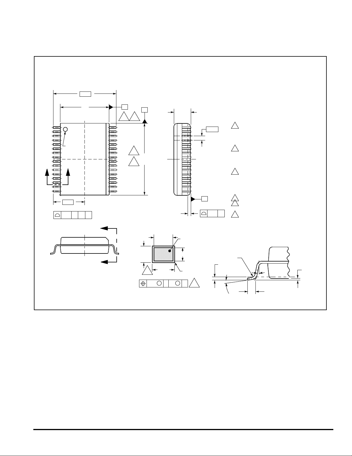
PACKAGE DIMENSIONS
DWB SUFFIX
32-LEAD SOIC WIDE BODY
PLASTIC PACKAGE
CASE 1324-02
ISSUE A
10.3
7.6
7.4
1
PIN 1 ID
nc...
I
BB
16
5.15
2X 16 TIPS
0.3 A
B C
A
A
cale Semiconductor,
C
32
17
B
95
4
11.1
10.9
9
(0.29)
0.25
0.19
0.38
6
0.22
0.13MCAMB
SECTION A-A
ROTATED 90 CLOCKWISE
°
2.65
2.35
BASE METAL
(0.203)
PLATING
30X
0.65
C
L
SEATING
A
PLANE
32X
0.10
R0.08 MIN
8
NOTES:
1. ALL DIMENSIONS ARE IN MILLIMETERS.
2. DIMENSIONING AND TOLERANCING PER ASME
Y14.5M, 1994.
3. DATUMS B AND C TO BE DETERMINED AT THE PLANE
WHERE THE BOTTOM OF THE LEADS EXIT THE
PLASTIC BODY.
4. THIS DIMENSION DOES NOT INCLUDE MOLD FLASH,
PROTRUSION OR GATE BURRS. MOLD FLASH,
PROTRUSION OR GATE BURRS SHALL NOT EXCEED
0.15 MM PER SIDE. THIS DIMENSION IS DETERMINED
AT THE PLANE WHERE THE BOTTOM OF T HE LEADS
EXIT THE PLASTIC BODY.
5. THIS DIMENSION DOES NOT INCLUDE INTERLEAD
FLASH OR PROTRUSIONS. INTERLEAD FLASH AND
PROTRUSIONS SHALL NOT EXCEED 0.25 MM PER
SIDE. THIS DIMENSION IS DETERMINED AT THE
PLANE WHERE THE BOTTOM OF TH E LEADS EXIT THE
PLASTIC BODY.
6. THIS DIMENSION DOES NOT INCLUDE DAMBAR
PROTRUSION. ALLOWABLE DAMBAR PROTRUSION
SHALL NOT CAUSE THE LEAD WIDTH TO EXCEED 0.4
MM PER SIDE. DAMBAR CANNOT BE LOCATED ON
THE LOWER RADIUS OR THE FOOT. MINIMUM SPACE
BETWEEN PROTRUSION AND ADJACENT LEAD
SHALL NOT LESS THAN 0.07 MM.
7. EXACT SHAPE OF EACH CORNER IS OPTIONAL.
8. THESE DIMENSIONS APPLY TO THE FLAT SECTION
OF THE LEAD BETWEEN 0.10 MM AND 0.3 MM FROM
A
0.25
GAUGE PLANE
THE LEAD TIP.
9. THE PACKAGE TOP MAY BE SMALLER THAN THE
PACKAGE BOTTOM. THIS DIMENSION IS
DETERMINED AT THE OUTERMOST EXTREMES OF
THE PLASTIC BODY EXCLU SIVE OF MOLD FLASH, TIE
BAR BURRS, GATE BURRS AND INTER-LEAD FLASH,
BUT INCLUDING ANY MISMATCH BETWEEN THE TOP
AND BOTTOM OF THE PLASTIC BODY.
°
0
MIN
0.9
°
8
0
0.5
°
SECTION B-B
0.29
0.13
Frees
MOTOROLA ANALOG INTEGRATED CIRCUIT DEVICE DATA 33702
For More Information On This Product,
Go to: www.freescale.com
23

Freescale Semiconductor, Inc.
nc...
I
cale Semiconductor,
Frees
Information in this document is provided solely to enable system and software implementers to use Motorola products. There are no express or implied
copyright licenses granted hereunder to design or fabricate any integrated circuits or integrated circuits based on the information in this document.
Motorola reserves the right to make changes without further notice to any products herein. Motorola makes no warranty, representation or guarantee
regarding the suitability of its products for any particular purpose, nor does Motorola assume any liability arising out of the application or use of any product
or circuit, and specifically disclaims any and all liability, including without limitation consequential or incidental damages. “Typical” parameters which may be
provided in Motorola data sheets and/or specifications can and do vary in different applications and actual performance may vary over time. All operating
parameters, including “Typicals” must be validated for each customer application by customer’s technical experts. Motorola does not convey any license
under its patent rights nor the rights of others. Motorola products are not designed, intended, or authorized for use as components in systems intended for
surgical implant into the body, or other applications intended to support or sustain life, or for any other application in which the failure of the Motorola product
could create a situation where personal injury or death may occur. Should Buyer purchase or use Motorola products for any such unintended or
unauthorized application, Buyer shall indemnify and hold Motorola and its officers, employees, subsidiaries, affiliates, and distributors harmless against all
claims, costs, damages, and expenses, and reasonable attorney fees arising out of, directly or indirectly, any claim of personal injury or death associated
with such unintended or unauthorized use, even if such claim alleges that Motorola was negligent regarding the design or manufacture of the part.
MOTOROLA and the Stylized M Logo are registered in the US Patent and Trademark Office. All other product or service names are the property of their
respective owners.
© Motorola, Inc. 2003
HOW TO REACH US:
USA/EUROPE/LOCATIONS NOT LISTED: JAPAN: Motorola Japan Ltd.; SPS, Technical Information Center
Motorola Literature Distribution 3-20-1 Minami-Azabu. Minato-ku, Tokyo 106-8573, Japan
P.O. Box 5405, Denver, Colorado 80217 81-3-3440-3569
1-800-521-6274 or 480-768-2130
ASIA/PACIFIC: Motorola Semiconductors H.K. Ltd.; Silicon Harbour Centre
2 Dai King Street, Tai Po Industrial Estate, Tai Po, N.T., Hong Kong
852-26668334
HOME PAGE: http://motorola.com/semiconductors
For More Information On This Product,
Go to: www.freescale.com
MC33702/D
 Loading...