查询MPC17550供应商
Freescale Semiconductor, Inc.
MOTOROLA
SEMICONDUCTOR TECHNICAL DATA
Document order number: MPC17550
Rev 1.0, 03/2004
Advance Information
17550
Quad H-Bridge Micromotor Driver
with DC/DC Boost Converter
The 17550 is a monolithic quad H-Bridge power IC ideal for portable
electronic applications containing tiny bipolar stepper motors and/or brush
DC-motors powered by two-to-four cell NiCd/NiMH batteries.
The 17550 operates from 2.5 V to 5.5 V, with independent control of each
H-Bridge via parallel 3.0 V or 5.0 V logic-compatible I/O. The device features
an on-board DC/DC boost converter that allows motor operation all the way
down to 1.6 V (the boost converter supplies the gate-drive voltage for each of
the four independent H-bridge output stages). Each output bridge has its own
gate-drive and logic circuitry with built-in shoot-through current protection.
nc...
I
The 17550 has four operating modes: Forward, Reverse, Brake, and
Tri-Stated (High Impedance). The 17550 has a low total R
@ 25°C. In addition, it can be set into a very low current-drain standby mode.
The H-Bridge outputs can be independently PWM’ed at up to 200 kHz for
speed/torque and current control. The 17550 can efficiently drive many types
of micromotors owing to its low output resistance and high output slew rates.
DS(ON)
of 1.2 Ω max
QUAD H-BRIDGE MICROMOTOR
DRIVER WITH DC/DC BOOST
CONVERTER
EV (Pb-FREE) SUFFIX
CASE 1522-01
36-LEAD VMFP
cale Semiconductor,
Frees
Features
• Low Total R
• Output Current 700 mA (Continuous per Output)
• Shoot-Through Current Protection Circuit
• PWM Control Input Frequency up to 200 kHz
• Built-In DC/DC Boost Converter
• Low Power Consumption Standby Mode
• Undervoltage Detection and Shutdown Circuit
• Pb-Free Packaging Designated by Suffix Code EV
0.7 Ω (Typ), 1.2 Ω (Max) @ 25°C
DS(ON)
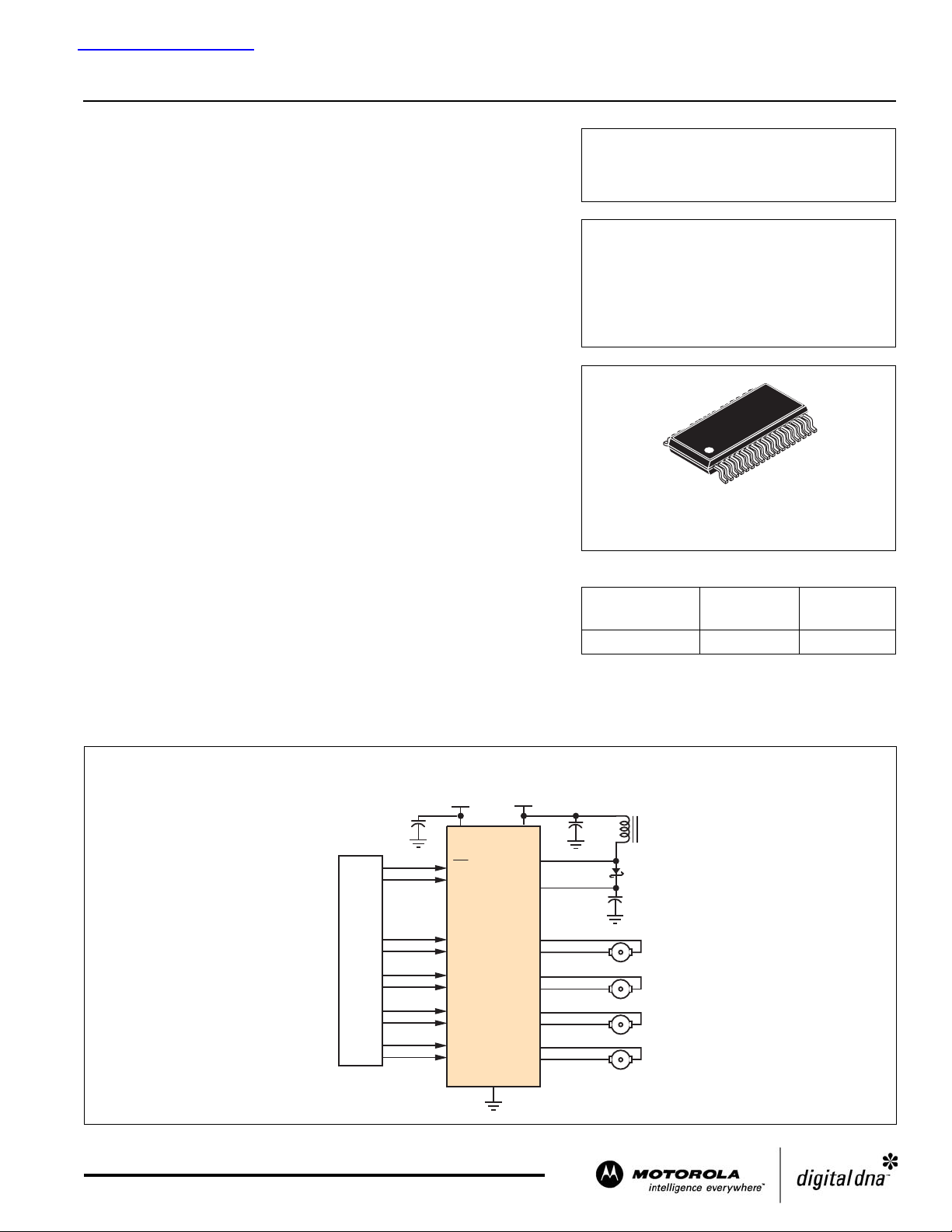
17550 Simplified Application Diagram
MCU
Simplified Application Diagram
V
M
VM
OE
PSB
INAF
INAR
INBF
INBR
INCF
INCR
INDF
INDR
17550
GND
V
V
DD
LX
VG
HBAF
HBAR
HBBF
HBBR
HBCF
HBCR
HBDF
HBDR
DD
ORDERING INFORMATION
Device
MPC17550EV/EL -10°C to 60°C 36 VMFP
Temperature
Range (T
)
A
Package
This document contains certain information on a new product.
Specifications and information herein are subject to change without notice.
© Motorola, Inc. 2004
For More Information On This Product,
Go to: www.freescale.com

Freescale Semiconductor, Inc.
GND
V
DD
PSB
INAF
INAR
nc...
I
INBF
INBR
LX VG
DC/DC
Converter
V
DD
VG
V
DD
V
DD
HBA
HBB
AGND
VMA
HBAF
HBAR
PGND
VMB
HBBF
cale Semiconductor,
Frees
OE
INCF
INCR
INDF
INDR
HBBR
V
DD
Control
Logic
Gate
Driver
and
Level
Shifter
PGND
HBC
VMC
HBCF
HBCR
PGND
HBD
VMD
HBDF
HBDR
PGND
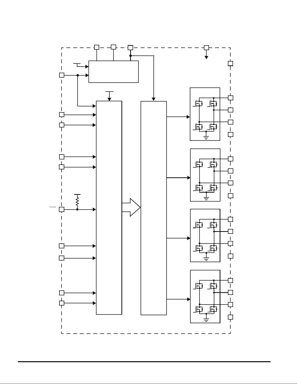
Figure 1. 17550 Simplified Internal Block Diagram
17550 MOTOROLA ANALOG INTEGRATED CIRCUIT DEVICE DATA
2
For More Information On This Product,
Go to: www.freescale.com

Freescale Semiconductor, Inc.
nc...
I
cale Semiconductor,
Frees
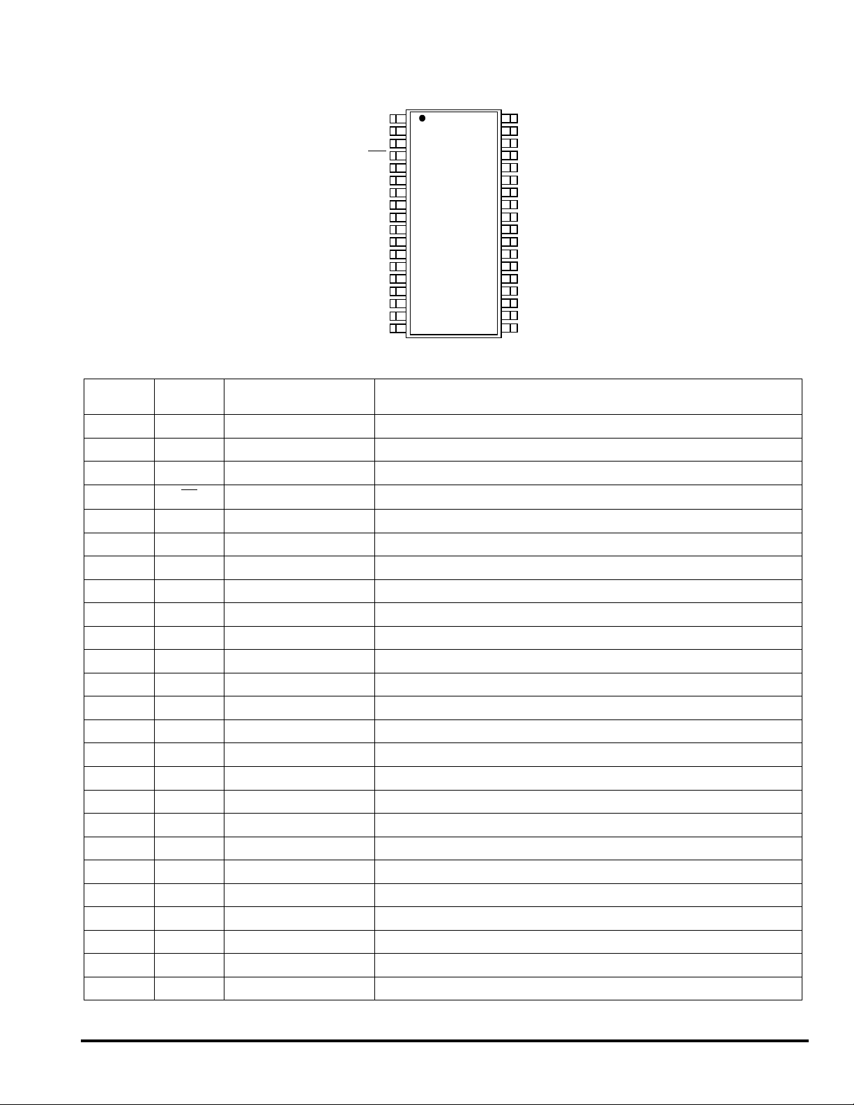
TERMINAL FUNCTION DESCRIPTION
Terminal
1 AGND Analog Ground
2 NC No Connect
3 PSB Power Standby
4 OE Output Enable
5, 9
6 HBAF HBA Forward Output
8 HBAR HBA Reverse Output
10, 14 VMB Motor Drive Power Supply B
11 HBBR HBB Reverse Output
7, 12, 25, 30 PGND Power Ground
13 HBBF HBB Forward Output
15 INAR Input Control HBA Reverse
16 INAF
17 INBF Input Control HBB Forward
18 INBR Input Control HBB Reverse
19 INDR Input Control HBD Reverse
20 INDF Input Control HBD Forward
21 INCF Input Control HBC Forward
22 INCR Input Control HBC Reverse
23, 27 VMD Motor Drive Power Supply D
24 HBDF HBD Forward Output
26 HBDR HBD Reverse Output
28, 32 VMC Motor Drive Power Supply C
29 HBCR HBC Reverse Output
31 HBCF HCB Forward Output
Terminal
Name
VMA Motor Drive Power Supply A
Formal Name Definition
Input Control HBA Forward Control signal input for H-Bridge A forward.
AGND
NC
PSB
OE
VMA
HBAF
PGND
HBAR
VMA
VMB
HBBR
PGND
HBBF
VMB
INAR
INAF
INBF
INBR
1
2
3
4
5
6
7
8
9
10
11
12
13
14
15
16
17
18
Analog and logic signal ground reference terminal.
No connection to this terminal.
Power standby mode control terminal.
Logic output Enable control of H-Bridges (Low = True).
Power supply voltage connection for Motor “A” (top of HBA).
Forward output of H-Bridge A.
Reverse output of H-Bridge A.
Power supply voltage connection for Motor “B” (top of HBB).
Reverse output of H-Bridge B.
Power ground connection.
Forward output of H-Bridge B.
Control signal input for H-Bridge A reverse.
Control signal input for H-Bridge B forward.
Control signal input for H-Bridge B reverse.
Control signal input for H-Bridge D reverse.
Control signal input for H-Bridge D forward.
Control signal input for H-Bridge C forward.
Control signal input for H-Bridge C reverse.
Power supply voltage connection for Motor “D” (top of HBD).
Forward output of H-Bridge D.
Reverse output of H-Bridge D.
Power supply voltage connection for Motor “C” (top of HBC).
Reverse Output of H-Bridge C.
Forward Output of H-Bridge C.
36
VG
35
V
34
33
32
31
30
29
28
27
26
25
24
23
22
21
20
19
DD
LX
GND
VMC
HBCF
PGND
HBCR
VMC
VMD
HBDR
PGND
HBDF
VMD
INCR
INCF
INDF
INDR
MOTOROLA ANALOG INTEGRATED CIRCUIT DEVICE DATA 17550
For More Information On This Product,
Go to: www.freescale.com
3

Freescale Semiconductor, Inc.
TERMINAL FUNCTION DESCRIPTION (continued)
Terminal
Name
DD
Formal Name Definition
Transistor Output
Logic Supply
Supply
nc...
I
Terminal
33 GND Ground
34 LX DC/ DC Converter Switching
35 V
36 VG Gate-Driver Circuit Power
Control circuit ground terminal for DC/DC circuit ground.
Open-drain output of the internal DC/DC converter circuit.
Control circuit power supply terminal.
Input terminal for the gate-drive voltage.
cale Semiconductor,
Frees
17550 MOTOROLA ANALOG INTEGRATED CIRCUIT DEVICE DATA
4
For More Information On This Product,
Go to: www.freescale.com

Freescale Semiconductor, Inc.
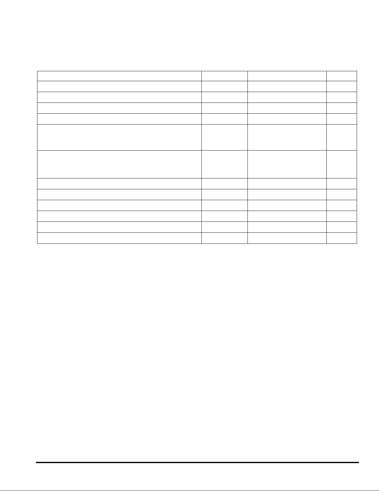
MAXIMUM RATINGS
All voltages are with respect to ground unless otherwise noted. Exceeding the ratings may cause a malfunction or permanent
damage to the device.
Rating Symbol Value Unit
Motor Supply Voltage
Gate-Driver Circuit Power Supply Voltage V
Logic Supply Voltage
Signal Input Voltage (Note 1)
Driver Output Current
Continuous (Note 2)
Peak (Note 3)
ESD Voltage
Human Body Model (Note 4)
nc...
I
cale Semiconductor,
Machine Model (Note 5)
Storage Temperature Range
Operating Ambient Temperature
Operating Junction Temperature
Thermal Resistance (Note 6) R
Power Dissipation (Note 7)
Soldering Temperature (Note 8) T
Notes
1. V
is the voltage level applied to any input terminal.
IN
is measured as the load current flowing through the H-bridge.
2. I
O
= 25°C, pulse width < 10 ms at intervals > 0.2 seconds.
3. T
A
4. ESD1 testing is performed in accordance with the Human Body Model (C
5. ESD2 testing is performed in accordance with the Machine Model (CZAP = 200 pF, RZAP = 0 Ω).
6. Mounted on 37 x 50 Cu area (1.6 mm FR-4 PCB).
7. Maximum at T
8. Soldering temperature limit is for 10 seconds maximum duration. Not designed for immersion soldering. Exceeding these limits may cause
malfunction or permanent damage to the device.
= 25°C.
A
V
M
G
V
DD
V
IN
I
O
I
OPK
V
ESD1
V
ESD2
T
STG
T
A
T
J
JA
θ
P
D
SOLDER
= 100 pF, R
ZAP
= 1500 Ω).
ZAP
-0.5 to 9.0 V
VDD-0.5 to 14 V
-0.5 to 6.0 V
-0.5 to VDD+0.5 V
0.7
2.0
±2000
±100
-65 to 150 °C
-10 to 60 °C
-10 to 150 °C
TBD °C/W
1500 mW
260 °C
A
V
Frees
MOTOROLA ANALOG INTEGRATED CIRCUIT DEVICE DATA 17550
For More Information On This Product,
Go to: www.freescale.com
5
 Loading...