

MOSYS M1T2HT18FL32E Datasheet
High Speed Flow-through 2-Mbit (64Kx32)
Standard 1T-SRAM
®
Embedded Memory Macro
M1T2HT18FL32E
M1T2HT18FL32E Rev 1_02 Page 1
© 2001 MoSys Inc., All Rights Reserved, 1020 Stewart Drive, Sunnyvale, CA 94085
• High Speed 1T-SRAM Standard Macro
• 100 MHz operation
• 1-Clock cycle time
• Flow-through read access timing
• Late write mode timing
• 32-Bit wide data buses
• Byte Write Enables
• Simple standard SRAM interface
• Fast delivery
• Ultra-Dense Memory
• 7.2mm
2
size per macro instance
• Redundancy & fuses included in macro area
• Silicon-Proven 1T-SRAM Technology
• Qualification programs completed
• Products in volume production
• High Yield and Reliability
• Built-in redundancy for enhanced yield
• Standard Logic Process
• TSMC 0.18µm CL018G process
• Logic design rules
• Uses 4 metal layers
• Routing over macro possible in layers 5+
• Power
• Single voltage 1.8V Supply
• Low power consumption
General Description
The M1T2HT18FL32E is a 2Mbit (2,169,152 bits), high speed, embedded 1T-SRAM macro. The
M1T2HT18FL32E is organized as 64K(65,536 words of 32 bits. T he m acro em ploys a flowthrough read tim ing
interface with late write timing. W rite contr ol over individual bytes in the input data is achieved through the use
of the byte write enable (bweb) input signals . The M1T2HT18FL32E m acro is implemented us ing MoSys 1TSRAM technology, resulting in extremely high density and performance.
High Speed Flow-through 2-Mbit (64Kx32)
Standard 1T-SRAM
®
Embedded Memory Macro
M1T2HT18FL32E
M1T2HT18FL32E Rev 1_02 Page 2
© 2001 MoSys Inc., All Rights Reserved, 1020 Stewart Drive, Sunnyvale, CA 94085
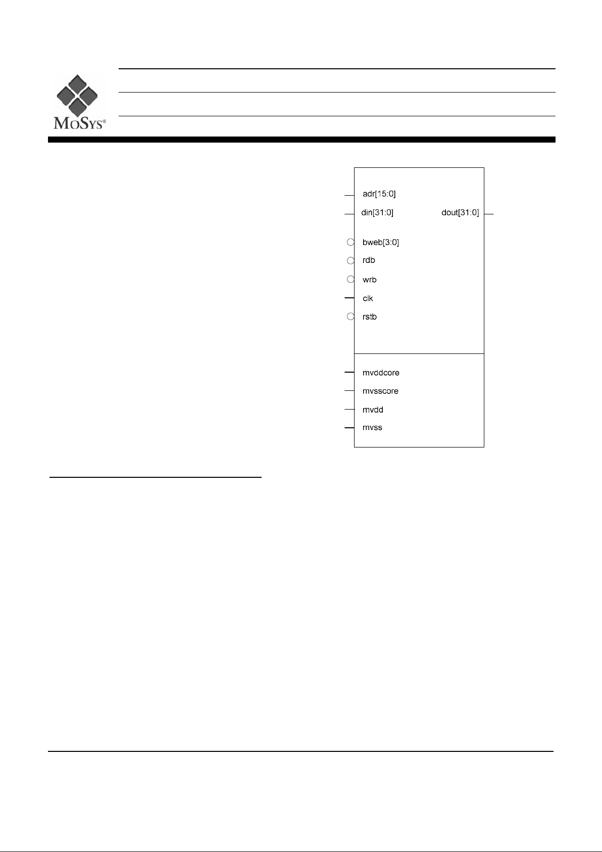
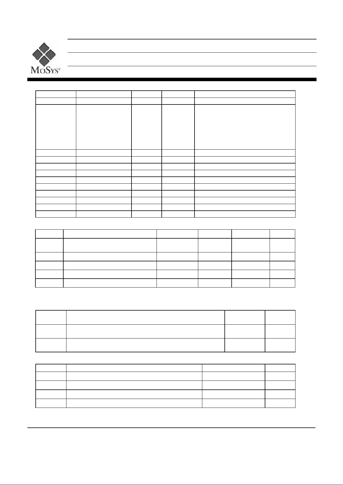
Memory Interface Signal List
Signal Name Valid Logic Direction Description
adr[15:0] Positive clk edge Positive Input Memory address
bweb[3:0] Positive clk edge Negative Input Memory byte write enables
bweb[n] = 0 enables data write
bweb[n] = 1 disables data write
bweb[3] controls writing of din[31:24]
bweb[2] controls writing of din[23:16]
bweb[1] controls writing of din[15:8]
bweb[0] controls writing of din[7:0]
rdb Positive clk edge Negative Input Memory read
wrb Positive clk edge Negative Input Memory write
din[31:0] Positive clk edge Positive Input Memory data in bus
dout[31:0] Positive clk edge Positive Output Memory data out bus
rstb Positive clk edge Negative Input Memory initialization reset
clk Clock Positive Input Memory Clock
mvddcore Memory core supply voltage
mvsscore Memory core ground
mvdd Memory interface supply voltage
mvss Memory interface ground
Recommended Operating Conditions
Symbol Parameter Condition Min Max Units
VDD Supply Voltage Range (1.8V
±10%)
Operating 1.62 1.98 V
TJ Junction Temperature Nominal VDD 0 125 °C
tCYC Cycle Time
Operating
5.0 33.3*
ns.
tCKH Clock High
Operating
0.45*tCYC 0.55*tCYC
ns.
tCKL Clock Low
Operating
0.45*tCYC 0.55*tCYC
ns.
Note: Minimum clock frequency limit adjustable to meet system timing requirements
Power Requirements
Symbol Condition
Current
per Instance
Units
I
DD1
Operating current, VDD=1.8V, clock frequency = 100MHz,
output not loaded, memory accessed every clock
0.85 mA/MHz
I
DD2
Standby current, VDD =1.8V, clock frequency =100MHz,
memory not accessed
0.35 mA/MHz
Input Loading
Symbol Condition Load Capacitance Units
C
DIN
din signal input loading 0.1 pF
C
ADR
adr signal input loading 0.1 pF
C
CTL
rdb, wrb and bweb signal input loading 0.1 pF
C
CLK
clk signal input loading 1.0 pF
 Loading...