


Mosel Vitelic V62C3801024LL-70V, V62C3801024LL-70T, V62C3801024LL-70B, V62C3801024LL-55V, V62C3801024LL-55T Datasheet
...
1
2
3
4
5
6
7
8
9
16
15
14
13
12
11
10
A
8
A
9
A
11
A
13
WE
CE
2
A
15
Vcc
NC
A
16
A
14
A
12
A
7
A
6
A
5
A
4
32
31
30
29
28
27
26
25
24
17
18
19
20
21
22
23
CE1
A
10
OE
I/O
8
I/O
7
I/O
6
I/O
5
I/O
4
GND
I/O
3
I/O
2
I/O
1
A
0
A
1
A
2
A
3
1024
X
1024
ROW DECODER
SENSE AMP
INPUT BUFFER
COLUMN DECODER
CONTROL
CIRCUIT
I/O
7
I/O
0
OE
WE
CE1
CE2
A9A10A11A12A13A14A15A
16
A
8
A
7
A
6
A
5
A
4
A
3
A
2
A
1
A
0
V62C3801024L(L)
Ultra Low Power
128K x 8 CMOS SRAM
Features
• Ultra Low-power consumption
- Active: 30mA at 55ns
- Stand-by: 5
µA (CMOS input/output)
1 µA CMOS input/output, L version
• Single +2.7V to 3.3V Power Supply
• Equal access and cycle time
• 55/70/85/100 ns access time
• Easy memory expansion with CE1
, CE2
and OE
inputs
• 2.0V data retention mode
• TTL compatible, Tri-state input/output
• Automatic power-down when deselected
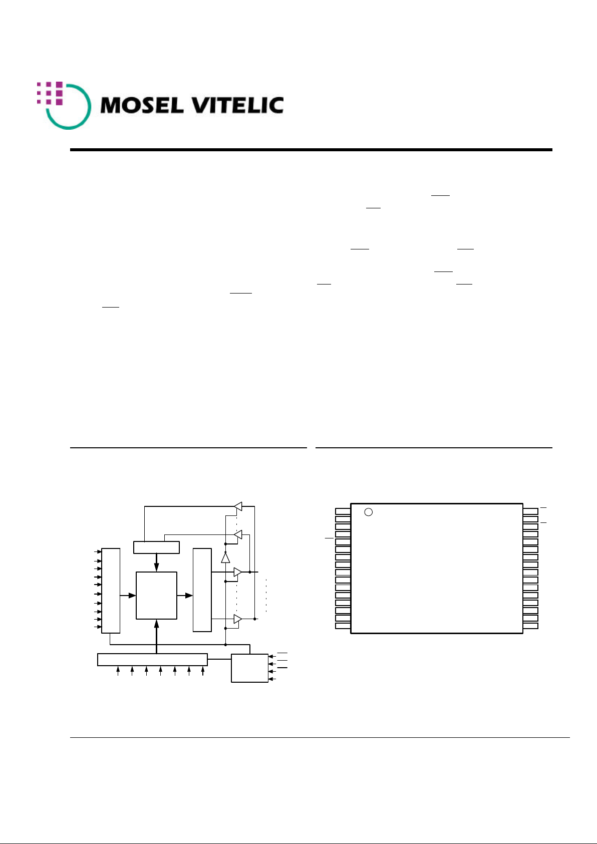
Functional Description
The V62C3801024L is a low power CMOS Static RAM organized as 131,072 words by 8 bits. Easy memory expansion is
provided by an active LOW CE1
, an active HIGH CE2, an a-
ctive LOW OE
, and Tri-state I/O’s. This device has an au-
tomatic power-down mode feature when deselected.
Writing to the device is accomplished by taking Chip E-
nable 1 (CE1
) with Write Enable (WE) LOW, and Chip Enable 2 (CE2) HIGH. Reading from the device is performed
by taking Chip Enable 1 (CE1
) with Output Enable
(OE) LOW while Write Enable (WE) and Chip Enable 2
(CE2) is HIGH. The I/O pins are placed in a high-impedance state when the device is deselected: the outputs are disabled during a write cycle.
The V62C3801024LL comes with a 2V data retention feature
and Lower Standby Power. TheV62C3801024L is available in
a 32-pin 8 x 20 mm TSOP1 / STSOP / 48-fpBGA packages.
32-Pin TSOP1 / STSOP (See next page)
Logic Block Diagram
1024
X
1024
ROW DECODER
SENSE AMP
INPUT BUFFER
COLUMN DECODER
CONTROL
CIRCUIT
I/O
8
I/O
1
OE
WE
CE1
CE2
A10A11A12A13A14A15A
16
A
8
A
7
A
6
A
5
A
4
A
3
A
2
A
1
A
0
A9
REV. 1.1 April 2001 V62C3801024L(L)
1
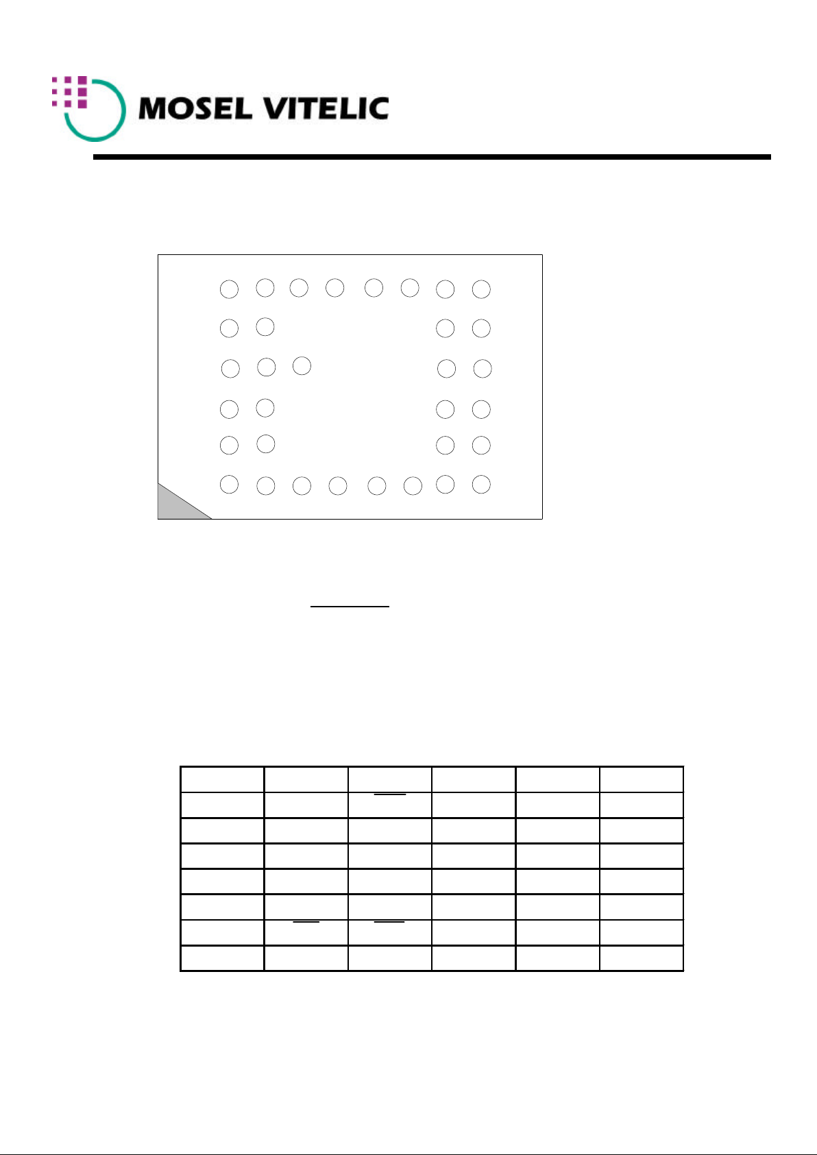
V62C3801024L(L)
2
Top View
48-CSP Ball-Grid Array package (shading indicates no ball)
1 2 3 4 5 6
A
A0A1CE2
A3A6A
8
B
I/O4A2WE
A4A7I/O
0
C
I/O5NCNCA5NC
I/O
1
D
VSSNCNCNCNCV
DD
E
VDDNCNCNCNCV
SS
F
I/O6NCNCNCNCI/O
2
G
I/O7OE
CE1A16A15I/O
3
H
A9A10A11A12A13A
14
MOSEL VITELIC V62C3801024L(L)B
TOP VIEW
6
5
4
3
2
1
A B C D E F G H
REV. 1.1 April 2001 V62C3801024L(L)
V62C3801024L(L)
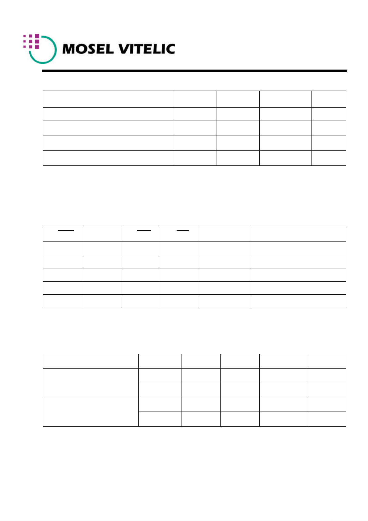
Absolute Maximum Ratings *
* Note: Stresses greater than those listed above Absolute Maximum Ratings may cause permanent damage to the device. This is a stress rating only and functional operation of the device at these or any conditions outside those indicated in the operational sections of this specification is not implied. Exposure to Absolute Maximum Rating conditions for extended periods may affect reliability.
Parameter Symbol Minimum Maximum Unit
Voltage on Any Pin Relative to Gnd Vt -0.5 4.6 V
Power Dissipation P
T
− 1.0 W
Storage Temperature (Plastic) Tstg -55 +150
0
C
Temperature Under Bias Tbias -40 +85
0
C
Truth Table
* Key: X = Don’t Care, L = Low, H = High
CE1 CE2 WE OE Data Mode
H X X X High-Z Standby
X L X X High-Z Standby
L H H L Data Out Active, Read
L H H H High-Z Active, Output Disable
L H L X Data In Active, Write
3
Recommended Operating Conditions (T
A
= 00C to +700C / -400C to 850C**)
* VIL min = -1.0V for pulse width less than tRC/2.
** For Industrial Temperature
Parameter Symbol Min Typ Max Unit
V
CC
2.7 3.0 3.3 V
Gnd 0.0 0.0 0.0 V
V
IH
2.2 - VCC + 0.5 V
V
IL
-0.5* - 0.6 V
Supply Voltage
Input Voltage
REV. 1.1 April 2001 V62C3801024L(L)