

Mosel Vitelic V61C3181024-15T, V61C3181024-15R, V61C3181024-12T, V61C3181024-12R, V61C3181024-10T Datasheet
...
MOSEL VITELIC
1
V61C3181024
128K X 8 HIGH SPEED
STATIC RAM
PRELIMINARY
V61C3181024 Rev. 1.3 February 1999
Features
■
High-speed: 10, 12, 15 ns
■
Fully static operation
■
All inputs and outputs directly TTL compatible
■
Three state outputs
■
Low data retention current (V
CC
= 2V)
■
Single 3.3V ± 0.3 Power Supply
■
Low CMOS Standby current of 5 mA max
■
Packages
– 32-pin TSOP
– 32-pin 300 mil SOJ
Description
The V61C3181024 is a 1,048,576-bit static
random-access memory organized as 131,072
words by 8 bits. Inputs and three-state outputs are
TTL compatible and allow for direct interfacing
with common system bus structures. The
V61C3181024 is available in 32-pin SOJ and
TSOP.
Device Usage Chart
Operating
Temperature
Range
Package Outline Access Time (ns)
Temperature
MarkT R 10 12 15
0 °
C to 70 ° C ••••• Blank
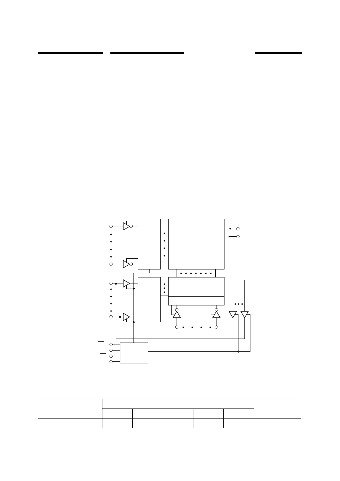
Functional Block Diagram
Row
Decoder
Memory Array
Input
Data
Circuit
Column I/O
Column Decoder
Control
Circuit
V
CC
GND
A
0
3181024 01
A
8
I/O
0
I/O
7
CE
2
OE
WE
CE
1
A
9
A
16
2
V61C3181024 Rev. 1.3 February 1999
MOSEL VITELIC
V61C3181024
Pin Descriptions
A
0
–A
16
Address Inputs
These 17 address inputs select one of the 128K x 8
bit segments in the RAM.
CE
1
, CE
2
Chip Enable Inputs
CE
1
is active LOW and CE
2
is active HIGH. Both
chip enables must be active to read from or write to
the device. If either chip enable is not active, the
device is deselected and is in a standby power
mode. The I/O pins will be in the high-impedance
state when deselected.
OE
Output Enable Input
The Output Enable input is active LOW. When OE
is LOW with CE LOW and WE HIGH, data of the
selected memory location will be available on the
I/O pins. When OE is HIGH, the I/O pins will be in
the high impedance state.
WE
Write Enable Input
An active LOW input, WE input controls read and
write operations. When CE and WE inputs are both
LOW, the data present on the I/O pins will be
written into the selected memory location.
I/O
0
–I/O
7
Data Input and Data Output Ports
These 8 bidirectional ports are used to read data
from and write data into the RAM.
V
CC
Power Supply
GND Ground
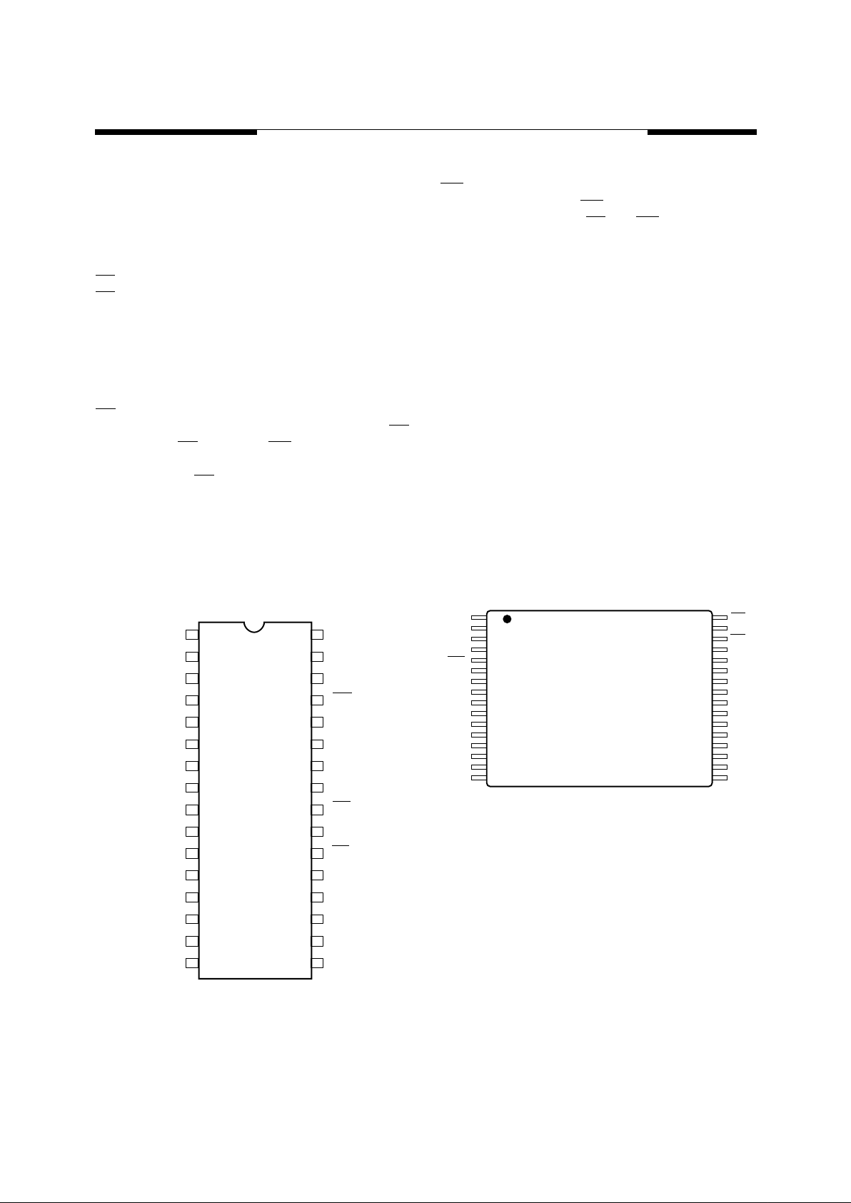
Pin Configurations (Top View)
32-Pin SOJ 32-Pin TSOP-I
1 32
3181024 02
2
31
3
30
4 29
5 28
6
27
7
26
8 25
9 24
10
23
11
22
12 21
13 20
14 19
15
18
16
17
A
10
A
9
A
8
A
7
A
6
A
5
A
4
A
3
A
2
A
1
A
0
I/O
0
I/O
1
I/O
2
GND
NC
A
11
CE
2
WE
A
12
A
13
A
14
A
15
OE
A
16
CE
1
I/O
7
I/O
6
I/O
5
I/O
4
I/O
3
V
CC
1
2
3
4
5
6
7
8
9
10
11
12
13
14
15
16
32
31
30
29
28
27
26
25
24
23
22
21
20
19
18
17
3181024 03
A15
A14
A13
A12
A11
VCC
NC
A10
A9
A8
A7
A6
A5
A4
A16
CE2
WE
I/O6
I/O7
I/O5
I/O4
I/O3
OE
I/O1
I/O2
VSS
CE1
I/O0
A0
A1
A2
A3
MOSEL VITELIC
V61C3181024
3
V61C3181024 Rev. 1.3 February 1999
Part Number Information
Absolute Maximum Ratings
(1)
NOTE:
1. Stresses greater than those listed under “Absolute Maximum Ratings” may cause permanent damage to the device. This is a stress
rating only and functional operation of the device at these or any other conditions above those indicated in the operational sections
of this specification is not implied. Exposure to absolute maximum rating conditions for extended periods may affect
reliability.
Symbol Parameter Commercial Units
V
N
Input Voltage -0.5 to V
CC
+ 0.5 V
V
DQ
Input/Output Voltage Applied V
CC
+ 0.5 V
T
BIAS
Temperature Under Bias -10 to +125
°
C
T
STG
Storage Temperature -65 to +150
°
C
SRAM
FAMILY
C = CMOS PROCESS
61 = HIGH SPEED
31 = 3.3V
OPERATING
VOLTAGE
1024K
ORGANIZATION
PKG
SPEED
3181024 05
PWR.
61 C 831 1024 –
MOSEL-VITELIC
V
8 = 8-bit
10 ns
12 ns
15 ns
TEMP.
BLANK = 0°C to 70°C
BLANK = STANDARD
T = TSOP STANDARD
R = 300 mil SOJ
DENSITY
Capacitance*
T
A
= 25 ° C, f = 1.0MHz
NOTE:
1. This parameter is guaranteed by design and not tested.
Truth Table
NOTE:
X = Don’t Care, L = LOW, H = HIGH
Symbol Parameter Conditions Max. Unit
C
IN
Input Capacitance V
IN
= 0V 6 pF
C
OUT
Output Capacitance V
I/O
= 0V 8 pF
Mode CE
1
CE
2
OE
WE
I/O
Operation
Standby H X X X High Z
Standby X L X X High Z
Output Disable L H H H High Z
Read L H L H D
OUT
Write L H X L D
IN
 Loading...