


Mosel Vitelic V58C265164S Datasheet
■
■
■
■
■
■
■
■
■
■
■
■
■
■
■
■
■
■
MOSEL VITELIC
V58C265164S
64 Mbit DDR SDRAM
2.5 VOLT 4M X 16
System Frequency (f
Clock Cycle Time (t
Clock Cycle Time (t
Clock Cycle Time (t
Features
4 banks x 1Mbit x 16 organization
High speed data transfer rates with system
frequency up to 250 MHz
Data Mask for Write Control (DM)
Four Banks controlled by BA0 & BA1
Programmable CAS Latency: 2, 2.5, 3
Programmable Wrap Sequence: Sequential
or Interleave
Programmable Burst Length:
2, 4, 8 for Sequential Type
2, 4, 8 for Interleave Type
Automatic and Controlled Precharge Command
Suspend Mode and Power Down Mode
Auto Refresh and Self Refresh
Refresh Interval: 4096 cycles/64 ms
Available in 66-pin 400 mil TSOP-II
SSTL-2 Compatible I/Os
Double Data Rate (DDR)
Bidirectional Data Strobe (DQs) for input and
output data, active on both edges
On-Chip DLL aligns DQ and DQs transitions with
CLK transitions
Differential clock inputs CLK and CLK
Power supply 2.5V ± 0.2V
) 250 MHz 225 MHz 200 MHz 183 MHz
CK
) 4 ns 4.5 ns 5 ns 5.5 ns
CK3
) 4.8 ns 5.4 ns 6 ns 6.6 ns
CK2.5
) 6 ns 6.75 ns 7.5 ns 8.25 ns
CK2
PRELIMINARY
445555
Description
The V58C265164S is a four bank DDR DRAM
organized as 4 banks x 1Mbit x 16. The
V58C265164S achieves high speed data transfer
rates by employing a chip architecture that
prefetches multiple bits and then synchronizes the
output data to a system clock
All of the control, address, circuits are synchronized with the positive edge of an externally supplied clock. I/O transactions are possible on both
edges of DQS.
Operating the four memory banks in an interleaved fashion allows random access operation to
occur at a higher rate than is possible with standard
DRAMs. A sequential and gapless data rate is possible depending on burst length, CAS latency and
speed grade of the device.
Device Usage Chart
Operating
Temperature
Range
0°C to 70°C • • • • • • • Blank
V58C265164S Rev. 1.7 August 2001
Package Outline CLK Cycle Time (ns) Power
1
Temperature
MarkJEDEC 66 TSOP II -4 -45 -5 -55 Std. L
MOSEL VITELIC
66 Pin Plastic TSOP-II
PIN CONFIGURATION
Top View
DD
NC
NC
DD
NC
CS
NC
A0
A1
A2
A3
DD
1
2
0
3
4
1
5
2
6
7
3
8
4
9
10
5
11
6
12
13
7
14
15
DDR SDRAM
16
17
18
19
20
21
22
23
24
25
26
27
28
29
30
31
32
33
V
DQ
V
DDQ
DQ
DQ
V
SSQ
DQ
DQ
V
DDQ
DQ
DQ
V
SSQ
DQ
V
DDQ
LDQS
V
LDM
WE
CAS
RAS
BA0
BA1
A10/AP
V
64M
66
65
64
63
62
61
60
59
58
57
56
55
54
53
52
51
50
49
48
47
46
45
44
43
42
41
40
39
38
37
36
35
34
V
SS
DQ
15
V
SSQ
DQ
14
DQ
13
V
DDQ
DQ
12
DQ
11
V
SSQ
DQ
10
DQ
9
V
DDQ
DQ
8
NC
V
SSQ
UDQS
NC
V
REF
V
SS
UDM
CLK
CLK
CKE
NC
NC
A11
A9
A8
A7
A6
A5
A4
V
SS
V58C265164S
Pin Names
CLK, CLK
CKE Clock Enable
CS Chip Select
RAS Row Address Strobe
CAS Column Address Strobe
WE Write Enable
UDQS, LDQS Data Strobe (Bidirectional)
–A
A
0
11
BA0, BA1 Bank Select
DQ
–DQ
0
15
UDM, LDM Data Mask
V
DD
V
SS
V
DDQ
V
SSQ
NC Not connected
V
REF
Differential Clock Input
Address Inputs
Data Input/Output
Power (+2.5V)
Ground
Power for I/O’s (+2.5V)
Ground for I/O’s
Reference Voltage for Inputs
V58C265164S Rev. 1.7 August 2001
2
*
MOSEL VITELIC
Capacitance*
T
= 0 to 70 ° C, V
A
Symbol Parameter
C
I1
C
I2
C
IO
C
CLK
Note: Capacitance is sampled and not 100% tested.
Input Capacitance (A0 to A11) 5 pF
Input Capacitance
RAS
Output Capacitance (DQ) 6.5 pF
Input Capacitance (CCLK, CLK
Block Diagram
Column address
counter
= 2.5 V ± 0.2 V, f = 1 Mhz
CC
, CAS, WE, CS, CKE
Column Addresses
)4pF
Column address
buffer
Max. Unit
5pF
V58C265164S
Absolute Maximum Ratings*
Operating temperature range..................0 to 70 °C
Storage temperature range ................-55 to 150 °C
Input/output voltage.................. -0.3 to (V
Power supply voltage .......................... -0.3 to 4.6 V
Power dissipation ...........................................1.6 W
Data out current (short circuit).......................50 mA
*Note: Stresses above those listed under “Absolute Maximum
Ratings” may cause permanent damage of the device.
Exposure to absolute maximum rating conditions for
extended periods may affect device reliability.
Row Addresses
A0 - A11, BA0, BA1A0 - A7, AP, BA0, BA1
Row address
buffer
Refresh Counter
+0.3) V
CC
Row decoder
Memory array
Bank 0
4096 x 256
Column decoder
Sense amplifier & I(O) bus
x 16 bit
CLK, CLK
DQS
Row decoder
Memory array
Bank 1
4096 x 256
Column decoder
Sense amplifier & I(O) bus
DLL
Strobe
Gen.
x 16 bit
Column decoder
Sense amplifier & I(O) bus
Input buffer Output buffer
-IQ
I/Q
0
15
Data Strobe
Row decoder
Memory array
Bank 2
4096 x 256
x 16 bit
Row decoder
Memory array
Bank 3
4096 x 256
CS
x 16 bit
RAS
CAS
WE
Column decoder
Sense amplifier & I(O) bus
Control logic & timing generator
CLK
CLK
CKE
LDM
UDM
V58C265164S Rev. 1.7 August 2001
3
MOSEL VITELIC
V58C265164S
Signal Pin Description
Pin Type Signal Polarity Function
CLK
CLK
CKE Input Level Active High Activates the CLK signal when high and deactivates the CLK signal when low, thereby
CS Input Pulse Active Low CS enables the command decoder when low and disables the command decoder when
RAS, CAS WEInput Pulse Active Low When sampled at the positive rising edge of the clock, CAS, RAS, and WE define the
DQS Input/
A0 - A11 Input Level — During a Bank Activate command cycle, A0-A11 defines the row address (RA0-RA11)
Input Pulse Positive
Edge
Pulse Active High Active on both edges for data input and output.
Output
The system clock input. All inputs except DQs and DMs are sampled on the rising edge
of CLK.
initiates either the Power Down mode, Suspend mode, or the Self Refresh mode.
high. When the command decoder is disabled, new commands are ignored but previous
operations continue.
command to be executed by the SDRAM.
Center aligned to input data
Edge aligned to output data
when sampled at the rising clock edge.
During a Read or Write command cycle, A0-An defines the column address (CA0-CAn)
when sampled at the rising clock edge.CAn depends from the SDRAM organization:
8M x 8 SDRAM CAn = CA8 (Page Length = 512 bits)
In addition to the column address, A10(=AP) is used to invoke autoprecharge operation
at the end of the burst read or write cycle. If A10 is high, autoprecharge is selected and
BA0, BA1 defines the bank to be precharged. If A10 is low, autoprecharge is disabled.
During a Precharge command cycle, A10(=AP) is used in conjunction with BA0 and BA1
to control which bank(s) to precharge. If A10 is high, all four banks will be precharged
simultaneously regardless of state of BA0 and BA1.
BA0,
BA1
DQx Input/
DM Input Pulse Active High In Write mode, DM has a latency of zero and operates as a word mask by allowing input
VDD, VSS Supply Power and ground for the input buffers and the core logic.
VDDQ
VSSQ
VREF Input Level — SSTL Reference Voltage for Inputs
Input Level — Selects which bank is to be active.
Level — Data Input/Output pins operate in the same manner as on conventional DRAMs.
Output
data to be written if it is low but blocks the write operation if is high.
Supply ——Isolated power supply and ground for the output buffers to provide improved noise
immunity.
V58C265164S Rev. 1.7 August 2001
4
■
MOSEL VITELIC
V58C265164S
Functional Description
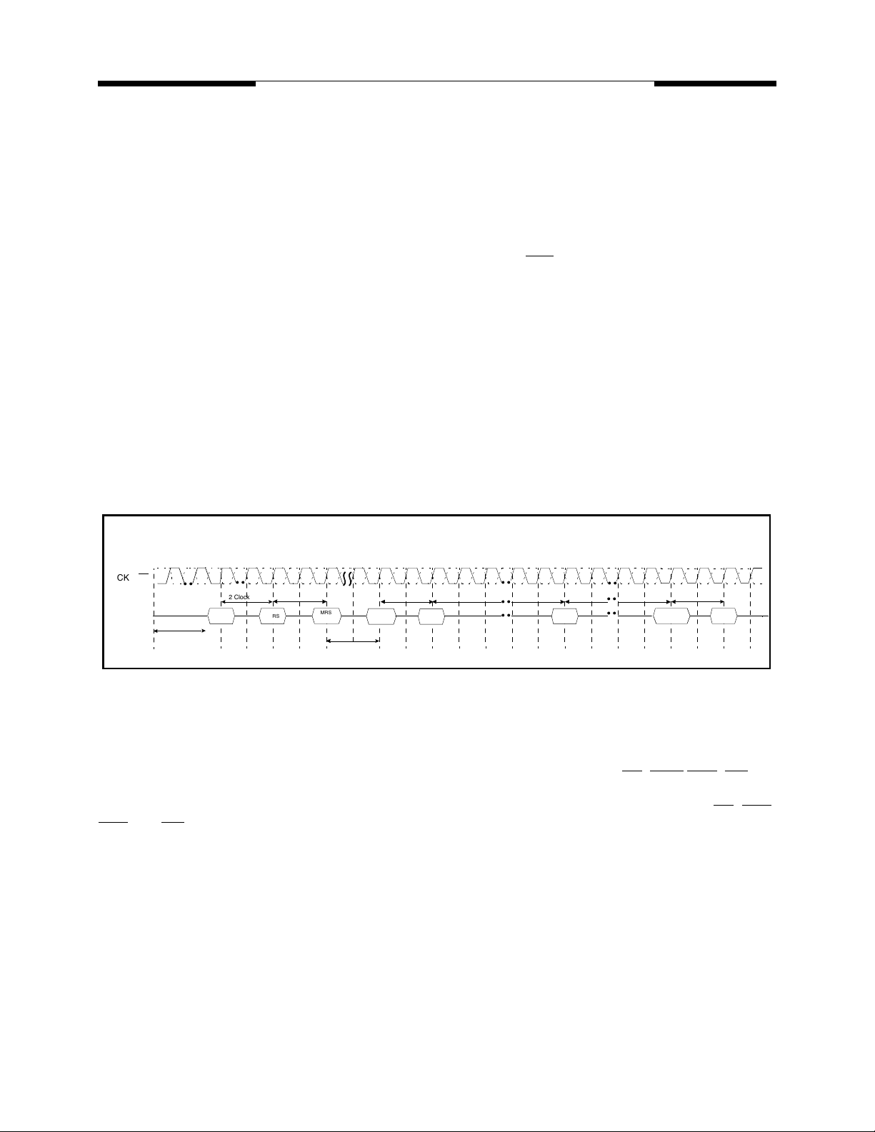
Power-Up Sequence
The following sequence is required for POWER UP.
1. Apply power and attempt to maintain CKE at a low state (all other inputs may be undefined.)
- Apply VDD before or at the same time as VDDQ.
- Apply VDDQ before or at the same time as VTT & Vref.
2. Start clock and maintain stable condition for a minimum of 200us.
3. The minimum of 200us after stable power and clock (CLK, CLK), apply NOP & take CKE high.
4. Precharge all banks.
5. Issue EMRS to enable DLL.(To issue “DLL Enable” command, provide “Low” to A0, “High” to BA0
and “Low” to all of the rest address pins, A1~A11 and BA1)
6. Issue a mode register set command for “DLL reset”. The additional 200 cycles of clock input is
required to lock the DLL. (To issue DLL reset command, provide “High” to A8 and “Low” to BA0)
7. Issue precharge commands for all banks of the device.
8. Issue 2 or more auto-refresh commands.
9. Issue a mode register set command to initialize device operation.
Note1 Every “DLL enable” command resets DLL. Therefore sequence 6 can be skipped during power up. Instead of it,
the additional 200 cycles of clock input is required to lock the DLL after enabling DLL.
Power up Sequence & Auto Refresh(CBR)
1 2 3 4 5 6 7 8 9 10 11 12 13 14 15 16 17 18 19
0
CK, CK
Command
••
200 µS Power up
to 1st command
precharge
ALL Banks
2 Clock min.
EMRS
t
precharge
ALL Banks
RP
1st Auto
Refresh
2 Clock min.
MRS
DLL Reset
min. 200 Cycle
654788
••••
t
RFC
••
••
2nd Auto
Refresh
••
t
RFC
••
••
Mode
Register Set
2 Clock min.
Any
Command
Extended Mode Register Set (EMRS)
The extended mode register stores the data for enabling or disabling DLL. The default value of the extended mode register is not defined, therefore the extended mode register must be written after power up for enabling or disabling DLL. The extended mode register is written by asserting low on CS, RAS, CAS, WE and
high on BA
the extended mode register). The state of address pins A
CAS and WE low is written in the extended mode register. Two clock cycles are required to complete the
write operation in the extended mode register. The mode register contents can be changed using the same
command and clock cycle requirements during operation as long as all banks are in the idle state. A
for DLL enable or disable. “High” on BA
must be set to low for proper EMRS operation. A
A
= 1 half strength. Refer to the table for specific codes.
1
(The DDR SDRAM should be in all bank precharge with CKE already high prior to writing into
0
is used for EMRS. All the other address pins except A
0
is used at EMRS to indicate I/O strength A
1
~ A
0
and BA
11
in the same cycle as CS, RAS,
1
is used
0
and BA
0
= 0 full strength,
1
0
V58C265164S Rev. 1.7 August 2001
5
MOSEL VITELIC
V58C265164S
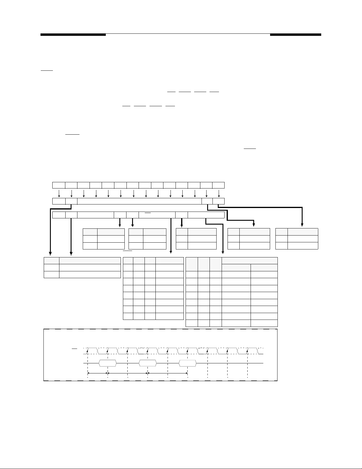
Mode Register Set (MRS)
The mode register stores the data for controlling the various operating modes of DDR SDRAM. It programs
CAS latency, addressing mode, burst length, test mode, DLL reset and various vendor specific options to
make DDR SDRAM useful for a variety of different applications. The default value of the mode register is not
defined, therefore the mode register must be written after EMRS setting for proper DDR SDRAM operation.
The mode register is written by asserting low on CS, RAS, CAS, WE and BA
in all bank precharge with CKE already high prior to writing into the mode register). The state of address pins
A
~ A
0
cycles are required to meet t
in the same cycle as CS, RAS, CAS, WE and BA0 low is written in the mode register. Two clock
11
spec. The mode register contents can be changed using the same com-
MRD
mand and clock cycle requirements during operation as long as all banks are in the idle state. The mode register is divided into various fields depending on functionality. The burst length uses A
uses A
mode during production test. A
, CAS latency (read latency from column address) uses A
3
is used for DLL reset. A
8
must be set to low for normal MRS operation. Refer
7
~ A
4
to the table for specific codes for various burst length, addressing modes and CAS latencies.
1. MRS can be issued only at all banks precharge state.
2. Minimum tRP is required to issue MRS command.
BA1 BA 0 A11 A 10 A9 A8 A7 A 6 A 5 A4 A 3 A 2 A1 A 0
0 RFU : Must be set "0"
MRS
0 TM CAS Latency BT Burst LengthRFU DLL
MRS
DLLI/O
(The DDR SDRAM should be
0
~ A
, addressing mode
0
. A
is a Mosel Vitelic specific test
6
7
Address Bus
Extended Mode Register
Mode Register
2
A8 DLL Reset
0No
1Yes
BA0 An ~ A0
0 (Existing)MRS Cycle
1 Extended Funtions(EMRS)
* RFU(Reserved for future use)
should stay "0" during MRS
cycle.
Mode Register Set
CK, CK
Command
Precharge
All Banks
tCK
A7 mode
0 Normal
1 Test
CAS
Latency
A6 A5 A4 Latency
0 0 0 Reserve
0 0 1 Reserve
01 0 2
01 1 3
1 0 0 Reserve
10 1
1 1 0 2.5
1 1 1 Reserve
201 534 867
Register Set
*2
tRP
*1
Mode
Reserve
t
MRD
A3 Burst Type
0 Sequential
1 Interleave
Burst Length
A2 A1 A0
0 0 0 Reserve Reserve
001 2 2
010 4 4
011 8 8
1 0 0 Reserve Reserve
1 0 1 Reserve Reserve
1 1 0 Reserve Reserve
1 1 1 Reserve Reserve
Any
Command
Sequential Interleave
A1 I/O Strength
0 Full
1 Half
Latency
A0 DLL Enable
0 Enable
1 Disable
V58C265164S Rev. 1.7 August 2001
6
MOSEL VITELIC
V58C265164S
Mode Register Set Timing
T5T0 T1 T2 T3 T4 T6 T7 T8
t
CK
CK
CK,
Command
Mode Register set (MRS) or Extended Mode Register Set (EMRS) can be issued only when all banks are in the idle state.
If a MRS command is issued to reset the DLL, then an additional 200 clocks must occur prior to issuing any new command
to allow time for the DLL to lock onto the clock.
Pre- All MRS/EMRS ANY
t
RP
t
MRD
T9
Burst Mode Operation
Burst Mode Operation is used to provide a constant flow of data to memory locations (Write cycle), or from
memory locations (Read cycle). Two parameters define how the burst mode will operate: burst sequence and
burst length. These parameters are programmable and are determined by address bits A
Mode Register Set command. Burst type defines the sequence in which the burst data will be delivered or
stored to the SDRAM. Two types of burst sequence are supported: sequential and interleave. The burst
length controls the number of bits that will be output after a Read command, or the number of bits to be input
after a Write command. The burst length can be programmed to values of 2, 4, or 8. See the Burst Length
and Sequence table below for programming information.
0
—A
during the
3
Burst Length and Sequence
Burst Length Starting Length (A
2
4
8
, A
, A
2
xx0 0, 1 0, 1
xx1 1, 0 1, 0
x00 0, 1, 2, 3 0, 1, 2, 3
x01 1, 2, 3, 0 1, 0, 3, 2
x10 2, 3, 0, 1 2, 3, 0, 1
x11 3, 0, 1, 2 3, 2, 1, 0
000 0,1, 2, 3, 4, 5, 6, 7 0,1, 2, 3, 4, 5, 6, 7
001 1, 2, 3, 4, 5, 6, 7, 0 1, 0, 3, 2, 5, 4, 7, 6
010 2, 3, 4, 5, 6, 7, 0, 1 2, 3, 0, 1, 6, 7, 4, 5
011 3, 4, 5, 6, 7, 0, 1, 2 3, 2, 1, 0, 7, 6, 5, 4
100 4, 5, 6, 7, 0, 1, 2, 3 4, 5, 6, 7, 0, 1, 2, 3
101 5, 6, 7, 0, 1, 2, 3, 4 5, 4, 7, 6, 1, 0, 3, 2
110 6, 7, 0, 1, 2, 3, 4, 5, 6 6, 7, 4, 5, 2, 3, 0, 1
111 7, 0, 1, 2, 3, 4, 5, 6 7, 6, 5, 4, 3, 2, 1, 0
) Sequential Mode Interleave Mode
1
0
V58C265164S Rev. 1.7 August 2001
7
MOSEL VITELIC
V58C265164S
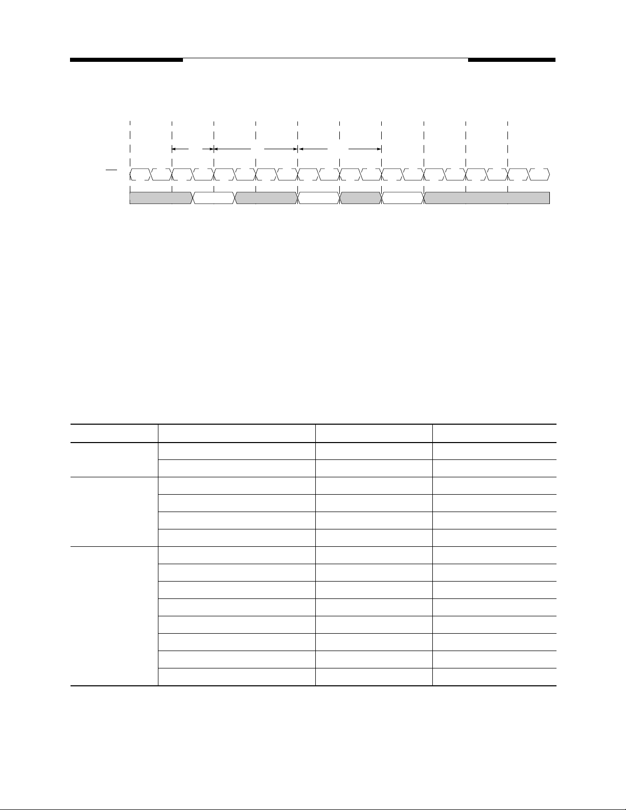
Bank Activate Command
The Bank Activate command is issued by holding CAS and WE high with CS and RAS low at the rising
edge of the clock. The DDR SDRAM has four independent banks, so two Bank Select addresses (BA
BA
) are supported. The Bank Activate command must be applied before any Read or Write operation can
1
and
0
be executed. The delay from the Bank Activate command to the first Read or Write command must meet or
exceed the minimum RAS to CAS delay time (t
min). Once a bank has been activated, it must be pre-
RCD
charged before another Bank Activate command can be applied to the same bank. The minimum time interval
between interleaved Bank Activate commands (Bank A to Bank B and vice versa) is the Bank to Bank delay
time (t
RRD
min).
Bank Activation Timing
(CAS Latency = 2; Burst Length = Any)
T0 T1 T2 T3 Tn Tn+1 Tn+2 Tn+3 Tn+4 Tn+5
t
CK, CK
BA/Address
Command
Bank/Row
Activate/A
t
RAS
t
RCD
(min)
(min)
Bank/Col
Read/A
RC
Bank
Pre/A
Bank/Row
Activate/A Activate/B
t
RRD
(min)tRP(min)
Bank/Row
Begin Precharge Bank A
Read Operation
With the DLL enabled, all devices operating at the same frequency within a system are ensured to have
the same timing relationship between DQ and DQS relative to the CK input regardless of device density, process variation, or technology generation.
The data strobe signal (DQS) is driven off chip simultaneously with the output data (DQ) during each read
cycle. The same internal clock phase is used to drive both the output data and data strobe signal off chip to
minimize skew between data strobe and output data. This internal clock phase is nominally aligned to the
input differential clock (CK, CK) by the on-chip DLL. Therefore, when the DLL is enabled and the clock frequency is within the specified range for proper DLL operation, the data strobe (DQS), output data (DQ), and
the system clock (CK) are all nominally aligned.
Since the data strobe and output data are tightly coupled in the system, the data strobe signal may be delayed
and used to latch the output data into the receiving device. The tolerance for skew between DQS and DQ
(t
) is tighter than that possible for CK to DQ (tAC) or DQS to CK (t
DQSQ
DQSCK
).
V58C265164S Rev. 1.7 August 2001
8
MOSEL VITELIC V58C265164S
Output Data (DQ) and Data Strobe (DQS) Timing Relative to the Clock (CK)
During Read Cycles
(CAS Latency = 2.5; Burst Length = 4)
T0 T1 T2 T3 T4
CK, CK
Command
DQS
DQ
READ NOP
NOP NOPNOP
t
(max)
DQSCK
t
(min)
DQSCK
tAC(min)
D
0
D
1
D
2
tAC(max)
D
3
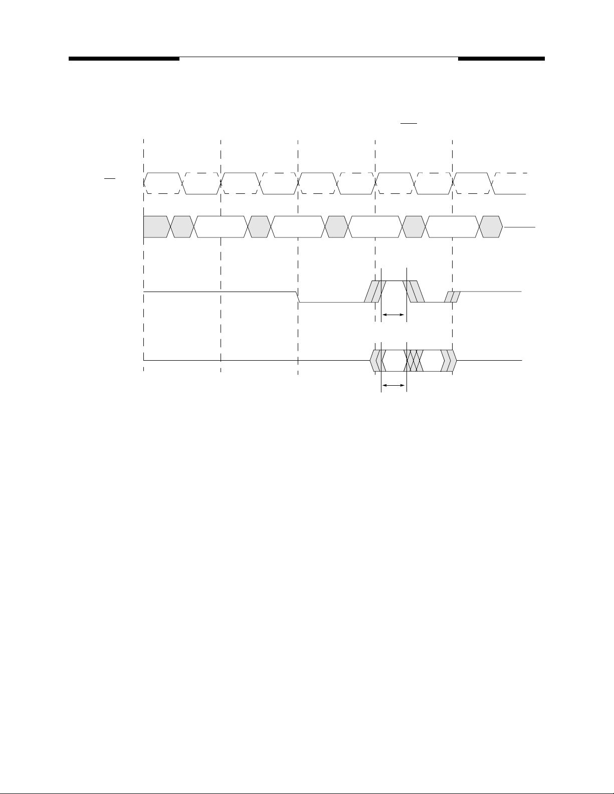
The minimum time during which the output data (DQ) is valid is critical for the receiving device (i.e., a memory controller device). This also applies to the data strobe during the read cycle since it is tightly coupled to
the output data. The minimum data output valid time (tDV) and minimum data strobe valid time (t
DQSV
) are derived from the minimum clock high/low time minus a margin for variation in data access and hold time due to
DLL jitter and power supply noise.
V58C265164S Rev. 1.7 August 2001
9
MOSEL VITELIC V58C265164S
Output Data and Data Strobe Valid Window for DDR Read Cycles
(CAS Latency = 2; Burst Length = 2)
T0 T1 T2 T3 T4
CK, CK
Command
DQS
DQ
READ NOP NOPNOP
t
DQSV
tDV(min)
(min)
D
0
D
1
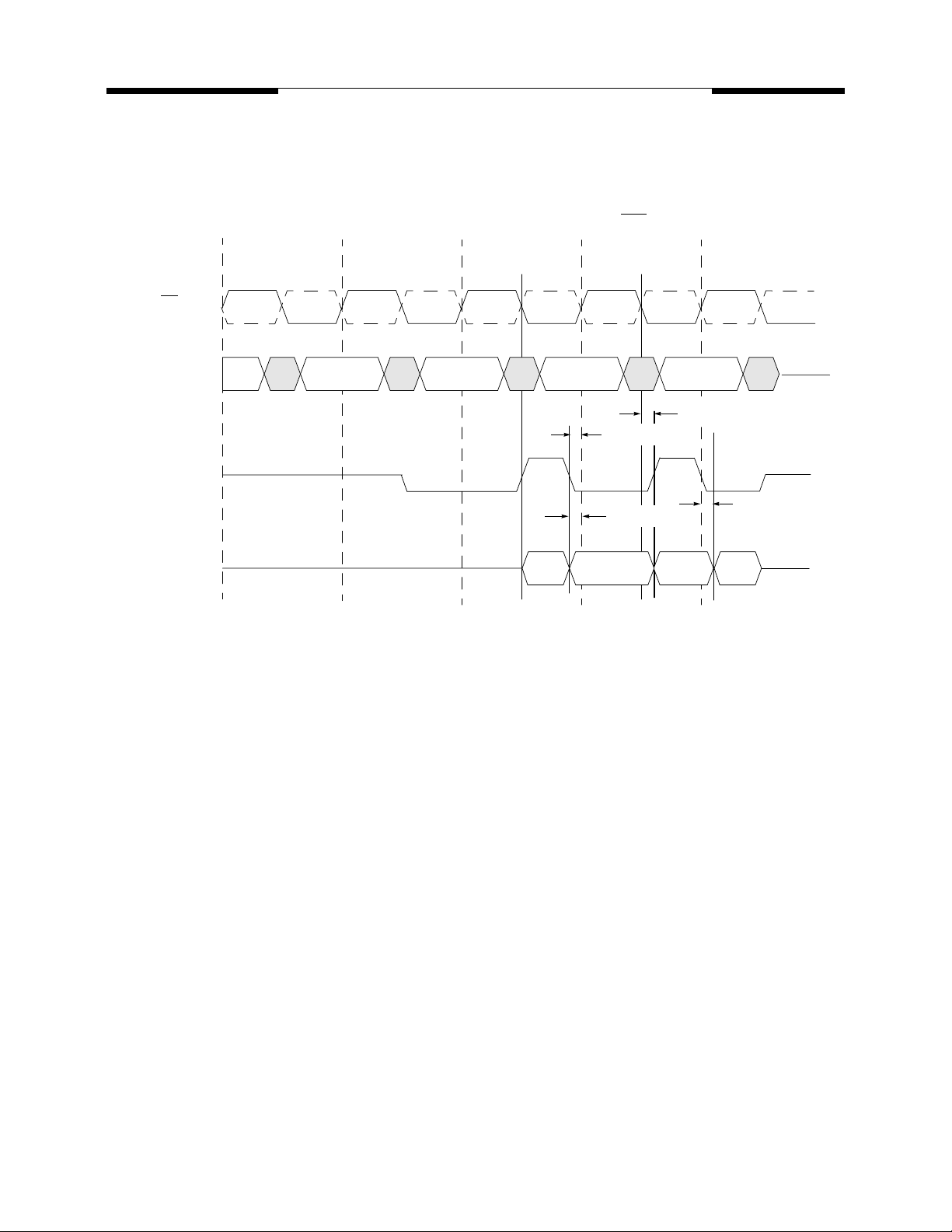
Read Preamble and Postamble Operation
Prior to a burst of read data and given that the controller is not currently in burst read mode, the data strobe
signal (DQS), must transition from Hi-Z to a valid logic low. The is referred to as the data strobe “read preamble” (t
valid data.
Once the burst of read data is concluded and given that no subsequent burst read operations are initiated,
the data strobe signal (DQS) transitions from a logic low level back to Hi-Z. This is referred to as the data
strobe “read postamble” (t
valid data.
Consecutive or “gapless” burst read operations are possible from the same DDR SDRAM device with no
requirement for a data strobe “read” preamble or postamble in between the groups of burst data. The data
strobe read preamble is required before the DDR device drives the first output data off chip. Similarly, the
data strobe postamble is initiated when the device stops driving DQ data at the termination of read burst cycles.
). This transition from Hi-Z to logic low nominally happens one clock cycle prior to the first edge of
RPRE
). This transition happens nominally one-half clock period after the last edge of
RPST
V58C265164S Rev. 1.7 August 2001
10
MOSEL VITELIC V58C265164S
Data Strobe Preamble and Postamble Timings for DDR Read Cycles
(CAS Latency = 2; Burst Length = 2)
T0 T1 T2 T3 T4
CK, CK
Command
READ NOP NOPNOP
t
(min)
RPRE
t
RPRE
(max)
t
RPST
(min)
DQS
t
(max)
RPST
DQ
t
DQSQ
(min)
D
0
t
DQSQ
D
1
(max)
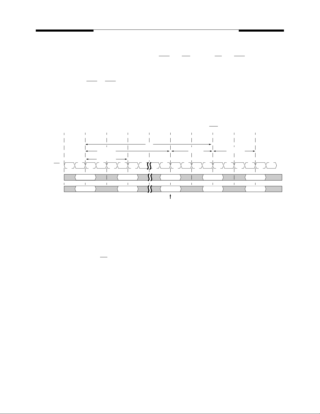
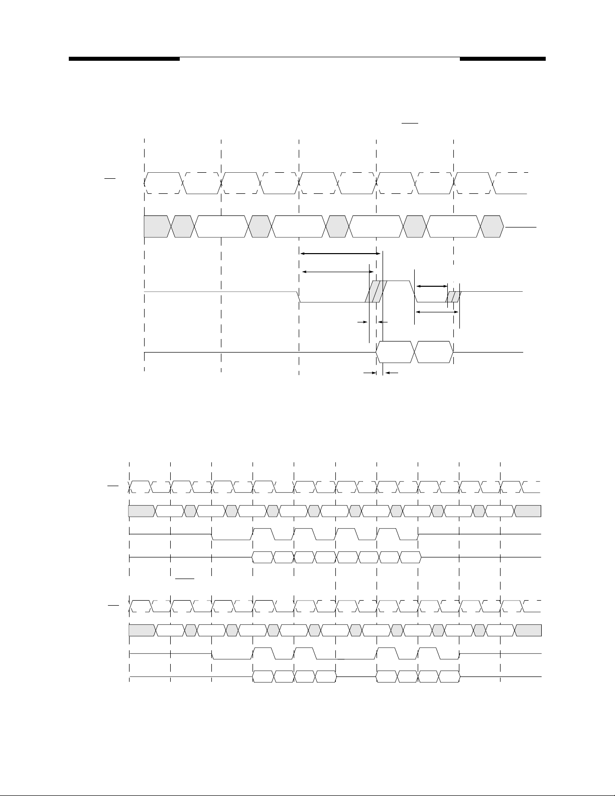
Consecutive Burst Read Operation and Effects on the Data Strobe Preamble and Postamble
Burst Read Operation (CAS Latency = 2; Burst Length = 4)
CK, CK
Command
A
NOP Read
NOP
B
NOP NOP NOP NOPRead
NOP
DQS
DQ
D0AD1
A
D2AD3
Burst Read Operation (CAS Latency = 2; Burst Length = 4)
CK, CK
Command
DQS
DQ
V58C265164S Rev. 1.7 August 2001
NOP Read
A
NOP
D0AD1
B
D2
A
11
AD3A
D0BD1BD2BD3
A
NOP NOP NOP NOPRead
D0BD1BD2BD3
B
NOP
B
MOSEL VITELIC V58C265164S
Auto Precharge Operation
The Auto Precharge operation can be issued by having column address A10 high when a Read or Write
command is issued. If A10 is low when a Read or Write command is issued, then normal Read or Write burst
operation is executed and the bank remains active at the completion of the burst sequence. When the Auto
Precharge command is activated, the active bank automatically begins to precharge at the earliest possible
moment during the Read or Write cycle once t
Read with Auto Precharge
If a Read with Auto Precharge command is initiated, the DDR SDRAM will enter the precharge operation
N-clock cycles measured from the last data of the burst read cycle where N is equal to the CAS latency programmed into the device. Once the autoprecharge operation has begun, the bank cannot be reactivated until
the minimum precharge time (t
) has been satisfied.
RP
Read with Autoprecharge Timing
(min) is satisfied.
RAS
(CAS Latency = 2; Burst Length = 4)
CK, CK
Command
DQS
DQ
T0 T1 T2 T3 T4 T5 T6 T7 T8
t
RAS
(min)
D0D1D2D
Begin Autoprecharge
t
(min)
RP
NOPBA R w/AP NOPNOP NOP NOP NOP BA
3
Earliest Bank A reactivate
T9
V58C265164S Rev. 1.7 August 2001
12
MOSEL VITELIC V58C265164S
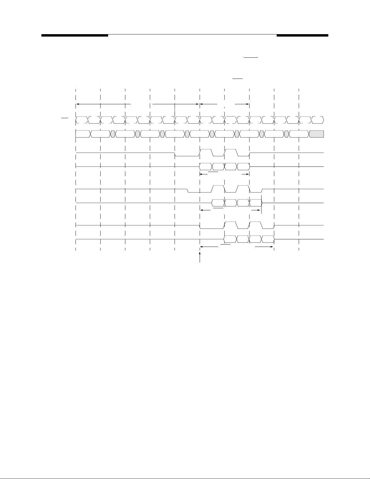
Read with Autoprecharge Timing as a Function of CAS Latency
(CAS Latency = 2, 2.5, 3; Burst Length = 4)
CK
CK,
Command
DQS
DQ
DQS
DQ
DQS
DQ
T0 T1 T2 T3 T4 T5 T6 T7 T8
t
BA NOP
RAS
(min)
Begin Autoprecharge
tRP(min)
D0D1D2D
CAS Latency=2
D0D1D2D
CAS Latency=2.5
D0D1D2D
CAS Latency=3
3
3
3
T9
NOPRAP NOPNOP NOP NOP BA NOP
V58C265164S Rev. 1.7 August 2001
13
MOSEL VITELIC V58C265164S
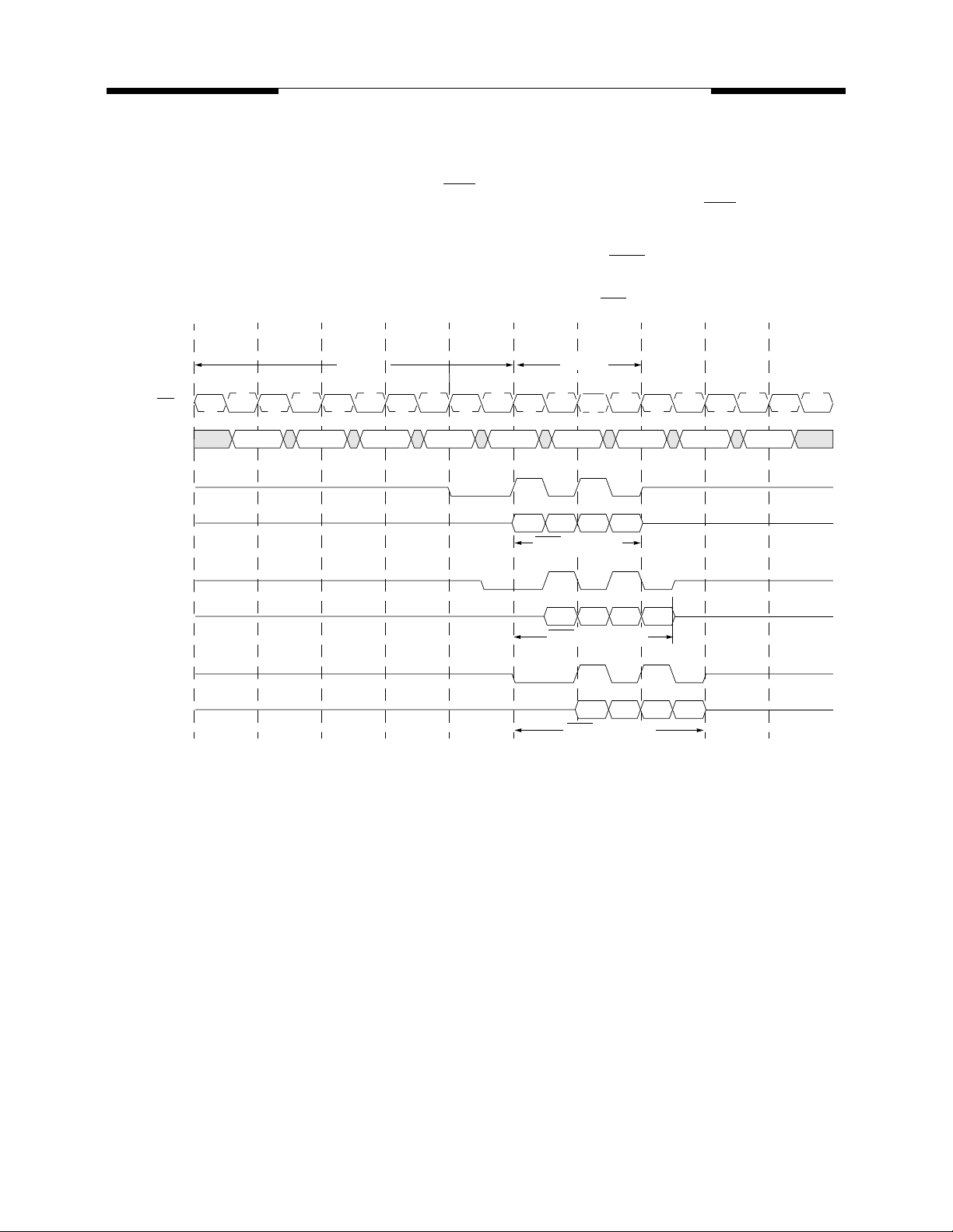
Precharge Timing During Read Operation
For the earliest possible Precharge command without interrupting a Read burst, the Precharge command
may be issued on the rising clock edge which is CAS latency (CL) clock cycles before the end of the Read
burst. A new Bank Activate (BA) command may be issued to the same bank after the RAS precharge time
(tRP). A Precharge command can not be issued until t
Read with Precharge Timing as a Function of CAS Latency
(min) is satisfied.
RAS
(CAS Latency = 2, 2.5, 3; Burst Length = 4)
CK
CK,
Command
DQS
DQ
DQS
DQ
DQS
DQ
T0 T1 T2 T3 T4 T5 T6 T7 T8
t
BA NOP
RAS
(min)
tRP(min)
NOP BA NOP
A
D0D1D2D
CAS Latency=2
D0D1D2D
CAS Latency=2.5
D0D1D2D
CAS Latency=3
3
3
3
T9
NOPRead NOPNOP Pre
V58C265164S Rev. 1.7 August 2001
14