


Mosel Vitelic V53C8125HT50, V53C8125HT45, V53C8125HT40, V53C8125HT35, V53C8125HT30 Datasheet
...
MOSEL VITELIC
1
V53C8125H
ULTRA-HIGH PERFORMANCE,
128K X 8 FAST PAGE MODE
CMOS DYNAMIC RAM
PRELIMINARY
HIGH PERFORMANCE 30 35 40 45 50
Max. RAS
Access Time, (t
RAC
) 30 ns 35 ns 40 ns 45 ns 50 ns
Max. Column Address Access Time, (t
CAA
) 16 ns 18 ns 20 ns 22 ns 24 ns
Min. Fast Page Mode Cycle Time, (t
PC
) 19 ns 21 ns 23 ns 25 ns 28 ns
Min. Read/Write Cycle Time, (t
RC
) 65 ns 70 ns 75 ns 80 ns 90 ns
Features
■
128K x 8-bit organization
■
RAS
access time: 30, 35, 40, 45, 50 ns
■
Fast Page Mode supports sustained data rates
up to 53 MHz
■
Read-Modify-Write, RAS
-Only Refresh,
CAS
-Before-RAS Refresh capability
■
Refresh Interval: 256 cycles/8 ms
■
Available in 26/24 pin 300 mil SOJ and 28 pin
TSOP-I packages
Description
The V53C8125H is a high speed 131,072 x 8 bit
CMOS dynamic random access memory. The
V53C8125H offers a combination of features: Fast
Page Mode for high data bandwidth, fast usable
speed, CMOS standby current.
All inputs and outputs are TTL compatible. Input
and output capacitances are significantly lowered to
allow increased system performance. Fast Page
Mode operation allows random access of up to 512
columns (x9) bits within a row with cycle times as
short as 19 ns. Because of static circuitry, the CAS
clock is not in the critical timing path. The flowthrough column address latches allow address
pipelining while relaxing many critical system timing
requirements for fast usable speed. These features
make the V53C8125H ideally suited for graphics,
digital signal processing and high performance peripherals.
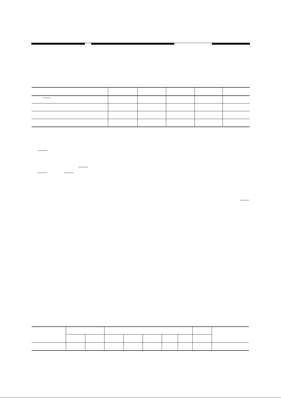
Device Usage Chart
Operating
Temperature
Range
Package Outline Access Time (ns) Power
Temperature
Mark
K T 30 35 40 45 50 Std.
0 °
C to 70 °
C . . . . . . . . Blank
V53C8125H Rev. 1.7 August 1998
2
MOSEL VITELIC
V53C8125H
V53C8125H Rev. 1.7 August 1998
FAMILY DEVICE PKG
(t
RAC
)
SPEED
PWR.
V53C 125
35 (35 ns)
40 (40 ns)
45 (45 ns)
50 (50 ns)
TEMP.
BLANK (0°C to 70°C)
BLANK (NORMAL)
K (SOJ)
T (TSOP)
H8
8125H 01
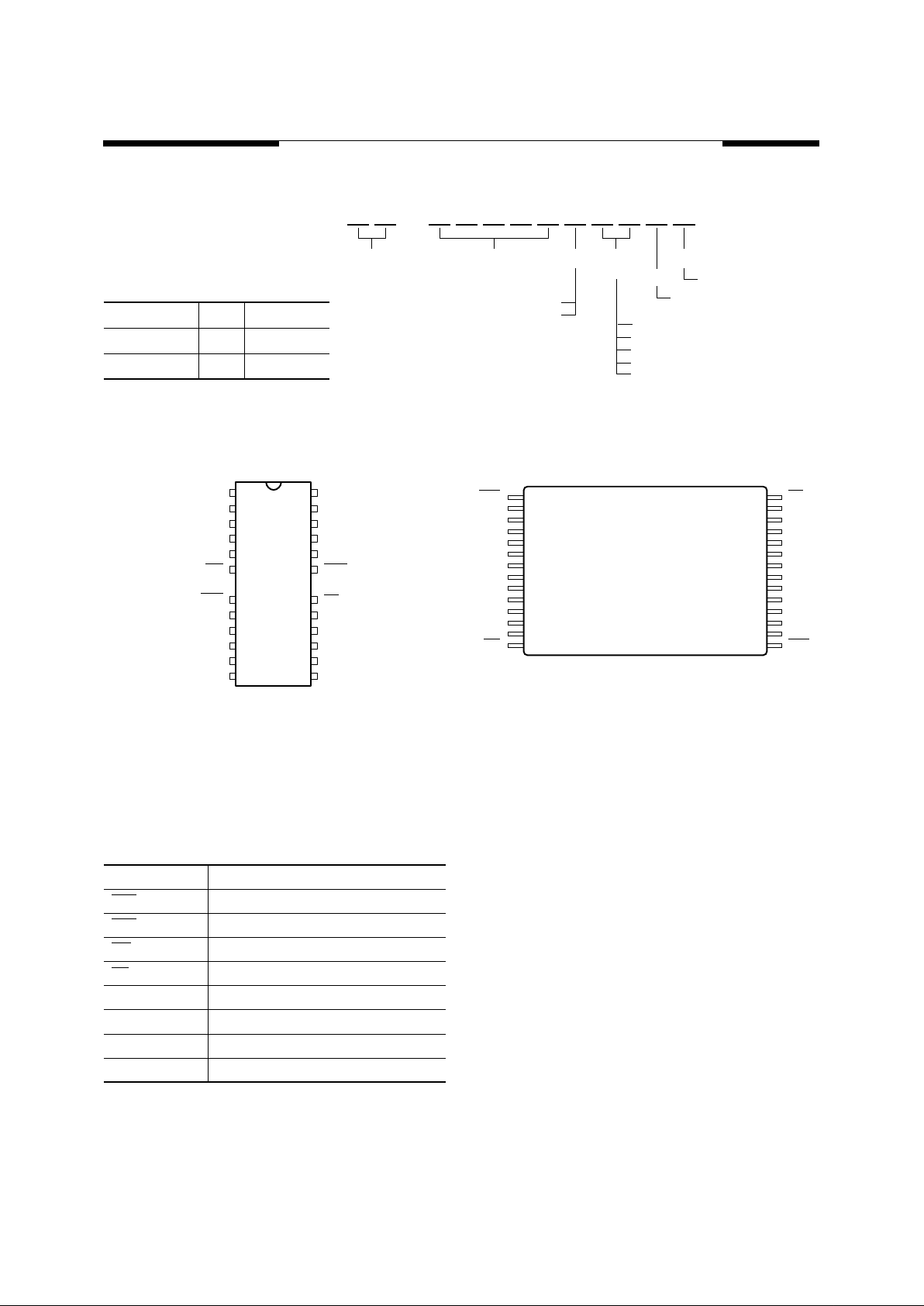
Pin Names
A
0
-A
8
Address Inputs (A
8
: Column Address only)
RAS
Row Address Strobe
CAS Column Address Strobe
WE Write Enable
OE Output Enable
I/O
1
- I/O
8
Data Input, Output
V
CC
+5V Supply
V
SS
0V Supply
NC No Connect
Description Pkg. Pin Count
SOJ K 26/24
TSOP-II T 28
26/24 Lead SOJ
PIN CONFIGURATION
Top View
28 Lead TSOP-I
PIN CONFIGURATION
Top View
V
SS
I/O
1
I/O
2
I/O
3
I/O
4
WE
RAS
A
0
A
1
A
2
A
3
V
CC
1
2
3
4
5
6
8
9
10
11
12
13
26
25
24
23
22
21
19
18
8125H 02
17
16
15
300 mil
V
SS
I/O
8
I/O
7
I/O
6
I/O
5
CAS
OE
A
8
A
7
A
6
A
5
A
4
14
CAS
I/O5
I/O6
I/O7
I/O8
VSS
VSS
NC
I/O1
I/O2
I/O3
I/O4
NC
WE
OE
A8
A7
A6
A5
A4
NC
VCC
NC
A3
A2
A1
A0
RAS
28
27
26
25
24
23
22
21
20
19
18
17
16
15
8125H 03
1
2
3
4
5
6
7
8
9
10
11
12
13
14
30 (30 ns)
MOSEL VITELIC
V53C8125H
3
V53C8125H Rev. 1.7 August 1998
Absolute Maximum Ratings*
Ambient Temperature
Under Bias................................. ñ10 ° C to +80 ° C
Storage Temperature (plastic)..... ñ55 ° C to +125 ° C
Voltage Relative to V
SS
.................ñ1.0 V to +7.0 V
Data Output Current .....................................50 mA
Power Dissipation..........................................1.0 W
*Note: Operation above Absolute Maximum Ratings can ad-
versely affect device reliability.
Capacitance*
T
A
= 25 ° C, V
CC
= 5 V ± 10%, V
SS
= 0 V
*Note: Capacitance is sampled and not 100% tested.
Symbol Parameter Typ. Max. Unit
C
IN1
Address Input 3 4 pF
C
IN2
RAS
, CAS, WE, OE 45pF
C
OUT
Data Input/Output 5 7 pF
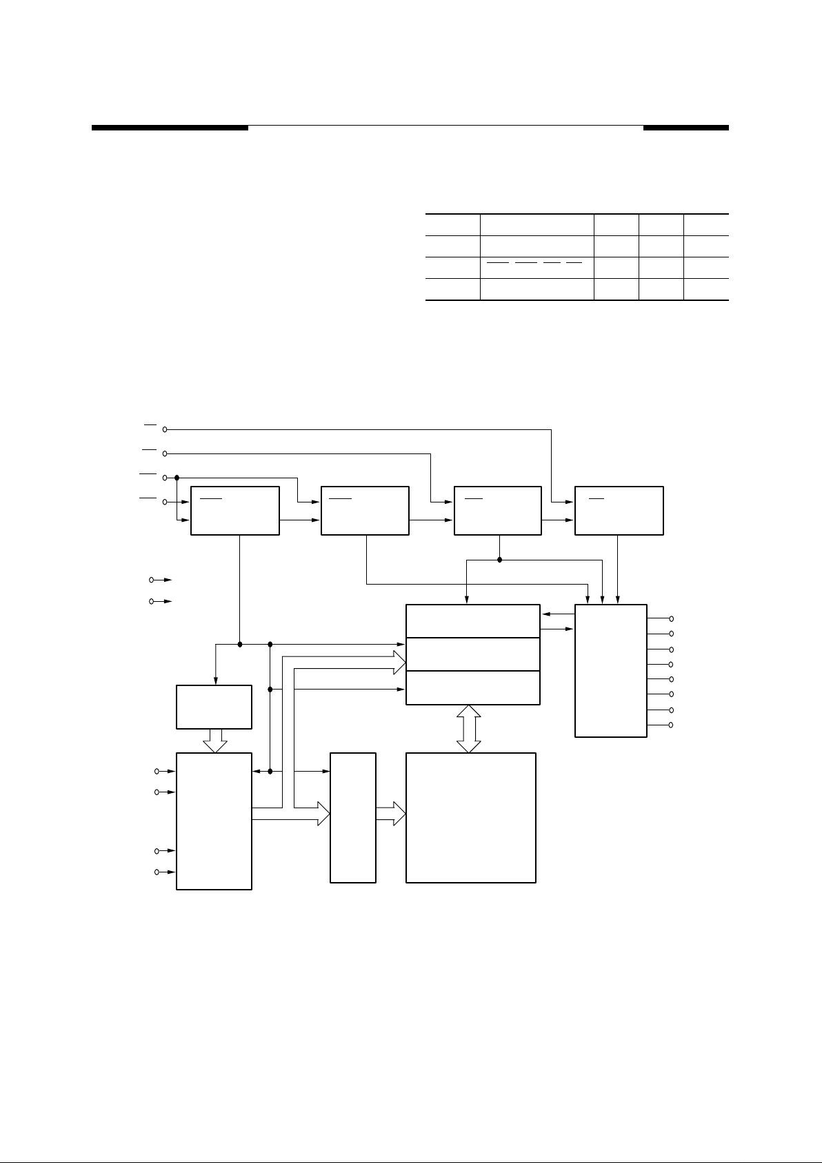
Block Diagram
A
0
A
1
A
7
A
8
SENSE AMPLIFIERS
REFRESH
COUNTER
V
CC
V
SS
9
8125H 16
I/O
1
ADDRESS BUFFERS
AND PREDECODERS
ROW
DECODERS
256
MEMORY
ARRAY
COLUMN DECODERS
DATA I/O BUS
Y0ñY
8
X0ñX
7
512 x 8
I/O
BUFFER
I/O
2
I/O
3
I/O
4
OE CLOCK
GENERATOR
WE CLOCK
GENERATOR
CAS CLOCK
GENERATOR
RAS CLOCK
GENERATOR
OE
128K x 8
WE
CAS
RAS
ï
ï
ï
I/O
5
I/O
6
I/O
7
I/O
8
4
V53C8125H Rev. 1.7 August 1998
MOSEL VITELIC
V53C8125H
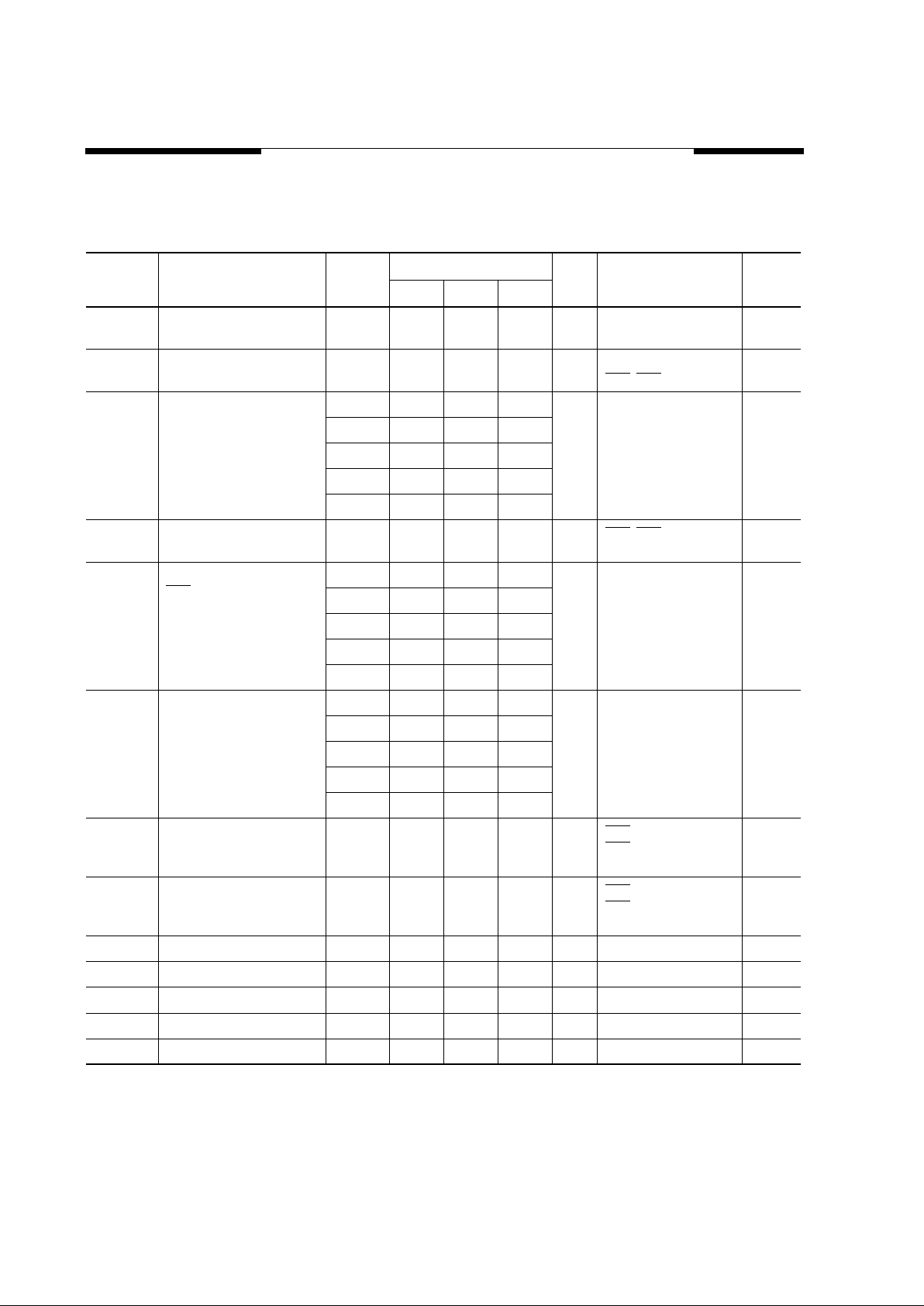
DC and Operating Characteristics
(1-2)
T
A
= 0 ° C to 70 ° C, V
CC
= 5 V ± 10%, V
SS
= 0 V, unless otherwise specified.
Symbol Parameter
Access
Time
V53C8125H
Unit Test Conditions NotesMin. Typ. Max.
I
LI
Input Leakage Current
(any input pin)
Ò10 10
µ
AV
SS
≤
V
IN
≤
V
CC
I
LO
Output Leakage Current
(for High-Z State)
Ò10 10
µ
AV
SS
≤
V
OUT
≤
V
CC
RAS
, CAS at V
IH
I
CC1
V
CC
Supply Current,
Operating
30 180 mA t
RC
= t
RC
(min.) 1, 2
35 160
40 150
45 145
50 135
I
CC2
V
CC
Supply Current,
TTL Standby
4 mA RAS
, CAS at V
IH
,
other inputs ≥ V
SS
I
CC3
V
CC
Supply Current,
RAS
-Only Refresh
30 180 mA t
RC
= t
RC
(min.) 2
35 160
40 150
45 145
50 135
I
CC4
V
CC
Supply Current,
Fast Page Mode Operation
30 110 mA Minimum Cycle 1, 2
35 95
40 90
45 85
50 80
I
CC5
V
CC
Supply Current,
Standby Output Enable
other inputs ≥ V
SS
2 mA RAS
= V
IH
CAS
= V
IL
1
I
CC6
V
CC
Supply Current,
CMOS Standby
1 mA RAS
≥ V
CC
Ò 0.2 V,
CAS
≥ V
CC
Ò 0.2 V,
All other inputs ≥ V
SS
V
CC
Supply Voltage 4.5 5.5 V
V
IL
Input Low Voltage Ò1 0.8 V 3
V
IH
Input High Voltage 2.4 V
CC
+ 1 V 3
V
OL
Output Low Voltage 0.4 V I
OL
= 4.2 mA
V
OH
Output High Voltage 2.4 2.4 V I
OH
= Ò5 mA
MOSEL VITELIC
V53C8125H
5
V53C8125H Rev. 1.7 August 1998
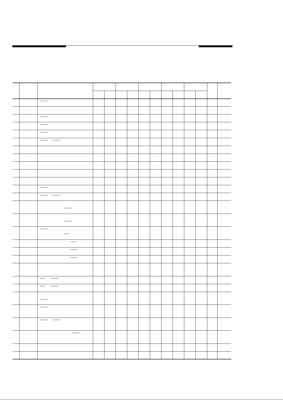
AC Characteristics
T
A
= 0 ° C to 70 ° C, V
CC
= 5 V ± 10%, V
SS
= 0V unless otherwise noted
AC Test conditions, input pulse levels 0 to 3V
# Symbol Parameter
30 35 40 45 50
Unit NotesMin. Max. Min. Max. Min. Max. Min. Max. Min. Max.
1t
RAS
RAS
Pulse Width 30 75K 35 75K 40 75K 45 75K 50 75K ns
2t
RC
Read or Write Cycle Time 65 70 75 80 90 ns
3t
RP
RAS
Precharge Time 25 25 25 25 30 ns
4t
CSH
CAS Hold Time 30 35 40 45 50 ns
5t
CAS
CAS Pulse Width 56789ns
6t
RCD
RAS to CAS Delay 15 20 16 24 17 28 18 32 19 36 ns
7t
RCS
Read Command Setup Time 00000ns4
8t
ASR
Row Address Setup Time 00000ns
9t
RAH
Row Address Hold Time 56789ns
10 t
ASC
Column Address Setup Time 00000ns
11 t
CAH
Column Address Hold Time 55567ns
12 t
RSH (R)
RAS Hold Time (Read Cycle) 10 10 10 10 10 ns
13 t
CRP
CAS to RAS Precharge Time 55555ns
14 t
RCH
Read Command Hold Time
Referenced to CAS
00 000ns5
15 t
RRH
Read Command Hold Time
Referenced to RAS
00000ns5
16 t
ROH
RAS Hold Time
Referenced to OE
678910ns
17 t
OAC
Access Time from OE 10 11 12 13 14 ns 12
18 t
CAC
Access Time from CAS 10 11 12 13 14 ns 6,7,14
19 t
RAC
Access Time from RAS 30 35 40 45 50 ns 6, 8, 9
20 t
CAA
Access Time from Column
Address
16 18 20 22 24 ns 6,7,10
21 t
LZ
OE or CAS to Low-Z Output 00000ns16
22 t
HZ
OE or CAS to High-Z Output 0506060708ns16
23 t
AR
Column Address Hold Time from
RAS
26 28 30 35 40 ns
24 t
RAD
RAS to Column Address
Delay Time
10 14 11 17 12 20 13 23 14 26 ns 11
25 t
RSH (W)
RAS or CAS Hold Time in
Write Cycle
10 10 10 10 10 ns
26 t
CWL
Write Command to CAS
Lead Time
10 11 12 13 14 ns
27 t
WCS
Write Command Setup Time 00000ns12, 13
28 t
WCH
Write Command Hold Time 55567ns
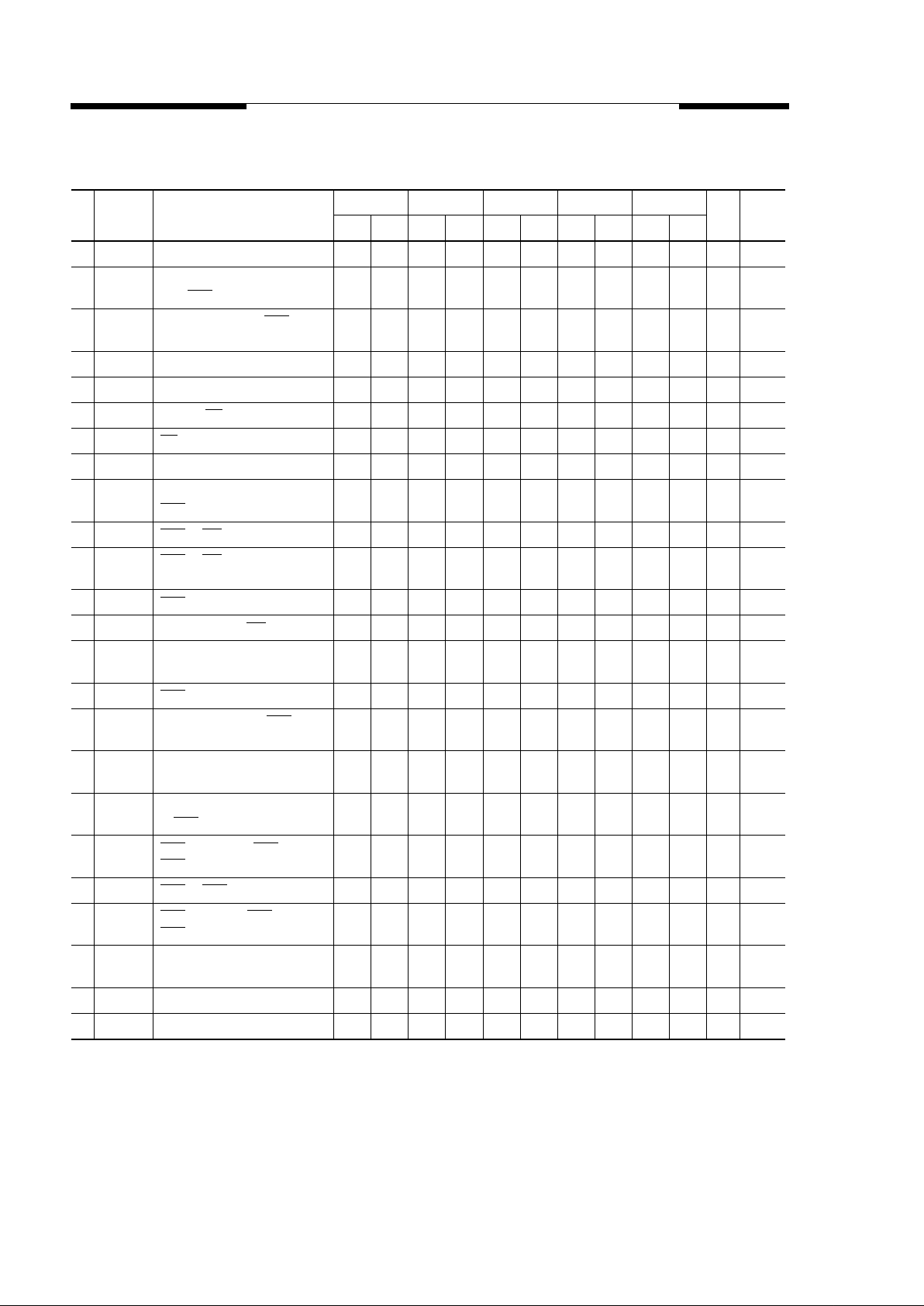
6
V53C8125H Rev. 1.7 August 1998
MOSEL VITELIC
V53C8125H
29 t
WP
Write Pulse Width 55567ns
30 t
WCR
Write Command Hold Time
from RAS
26 28 30 35 40 ns
31 t
RWL
Write Command to RAS
Lead Time
10 11 12 13 14 ns
32 t
DS
Data in Setup Time 00000ns14
33 t
DH
Data in Hold Time 55567ns14
34 t
WOH
Write to OE Hold Time 55678ns14
35 t
OED
OE to Data Delay Time 55678ns14
36 t
RWC
Read-Modify-Write Cycle Time 100 105 110 115 130 ns
37 t
RRW
Read-Modify-Write Cycle
RAS Pulse Width
65 70 75 80 87 ns
38 t
CWD
CAS to WE Delay 26 28 30 32 34 ns 12
39 t
RWD
RAS to WE Delay in ReadModify-Write Cycle
50 54 58 62 68 ns 12
40 t
CRW
CAS Pulse Width (RMW) 44 46 48 50 52 ns
41 t
AWD
Col. Address to WE Delay 32 35 38 41 42 ns 12
42 t
PC
Fast Page Mode Read
or Write Cycle Time
19 21 23 25 28 ns
43 t
CP
CAS Precharge Time 44567ns
44 t
CAR
Column Address to RAS
Setup Time
16 18 20 22 24 ns
45 t
CAP
Access Time from Column
Precharge
19 21 23 25 27 ns 7
46 t
DHR
Data in Hold Time Referenced
to RAS
26 28 30 35 40 ns
47 t
CSR
CAS Setup Time CAS- beforeRAS Refresh
10 10 10 10 10 ns
48 t
RPC
RAS to CAS Precharge Time 00000ns
49 t
CHR
CAS Hold Time CAS-beforeRAS Refresh
7 8 8 10 12 ns
50 t
PCM
Fast Page Mode Read-ModifyWrite Cycle Time
56 58 60 65 70 ns
51 t
T
Transition Time (Rise and Fall) 3 50 3 50 3 50 3 50 3 50 ns 15
52 t
REF
Refresh Interval (512 Cycles) 88888ms17
# Symbol Parameter
30 35 40 45 50
Unit NotesMin. Max. Min. Max. Min. Max. Min. Max. Min. Max.
AC Characteristics
(ContÌd)