

Mosel Vitelic V53C516400A Datasheet
■
■
■
■
■
■
■
■
■
0 °
MOSEL VITELIC
V53C516400A
PRELIMINARY
4M x 4 FAST PAGE MODE
CMOS DYNAMIC RAM
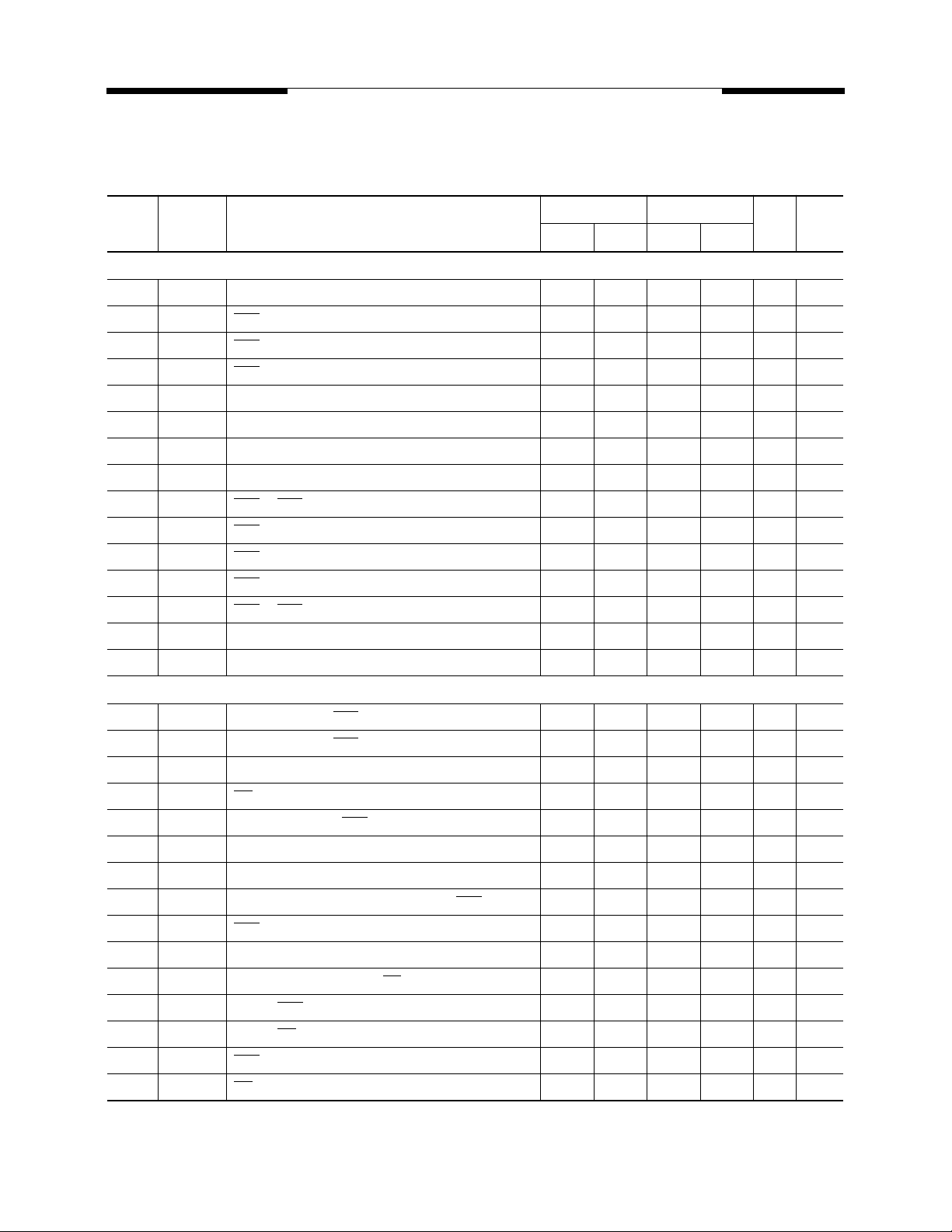
V53C516400A 50 60
Max. RAS
Max. Column Address Access Time, (t
Min. Page Mode Cycle Time, (t
Min. Read/Write Cycle Time, (t
Access Time, (t
Features
4M x 4-bit organization
Fast Page Mode for a sustained data rate
of 50 MHz
access time: 50, 60 ns
RAS
Low power dissipation
Read-Modify-Write, RAS-Only Refresh,
-Before-RAS Refresh and Hidden Refresh
CAS
Refresh Interval: 4096 cycles/64 ms
Available in 24/26-pin 300 mil SOJ,
and 24/26-pin 300 mil TSOP-II
Single +5V ± 10% Power Supply
TTL Interface
) 50 ns 60 ns
RAC
) 25 ns 30 ns
CAA
) 35 ns 40 ns
PC
) 84 ns 104 ns
RC
Description
The V53C516400A is a 4,194,304 x 4 bit highperformance CMOS dynamic random access memory. The V53C516400A offers Page mode operation. The V53C516400A has asymmetric address,
12-bit row and 10-bit column.
All inputs are TTL compatible. Fast Page Mode
operation allows random access up to 1024 x 4 bits,
within a page, with cycle times as short as 35ns.
These features make the V53C516400A ideally
suited for a wide variety of high performance computer systems and peripheral applications.
Device Usage Chart
Operating
Temperature
Range
C to 70 ° C • • • • • Blank
V53C516400A Rev. 1.1 March 1998
Package Outline Access Time (ns) Power
1
Temperature
MarkK T 50 60 Std.
MOSEL VITELIC
24/26-Pin Plastic SOJ/TSOP-II
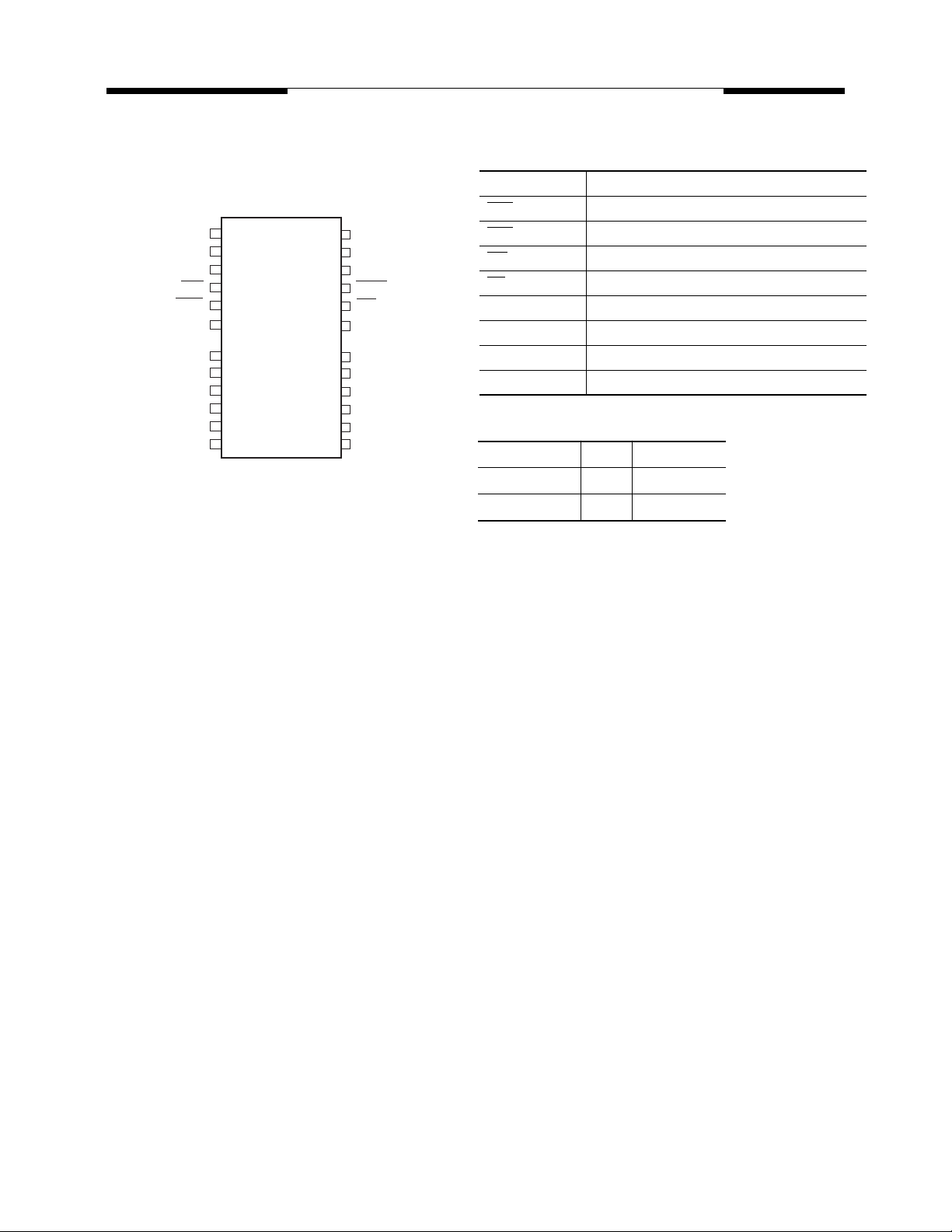
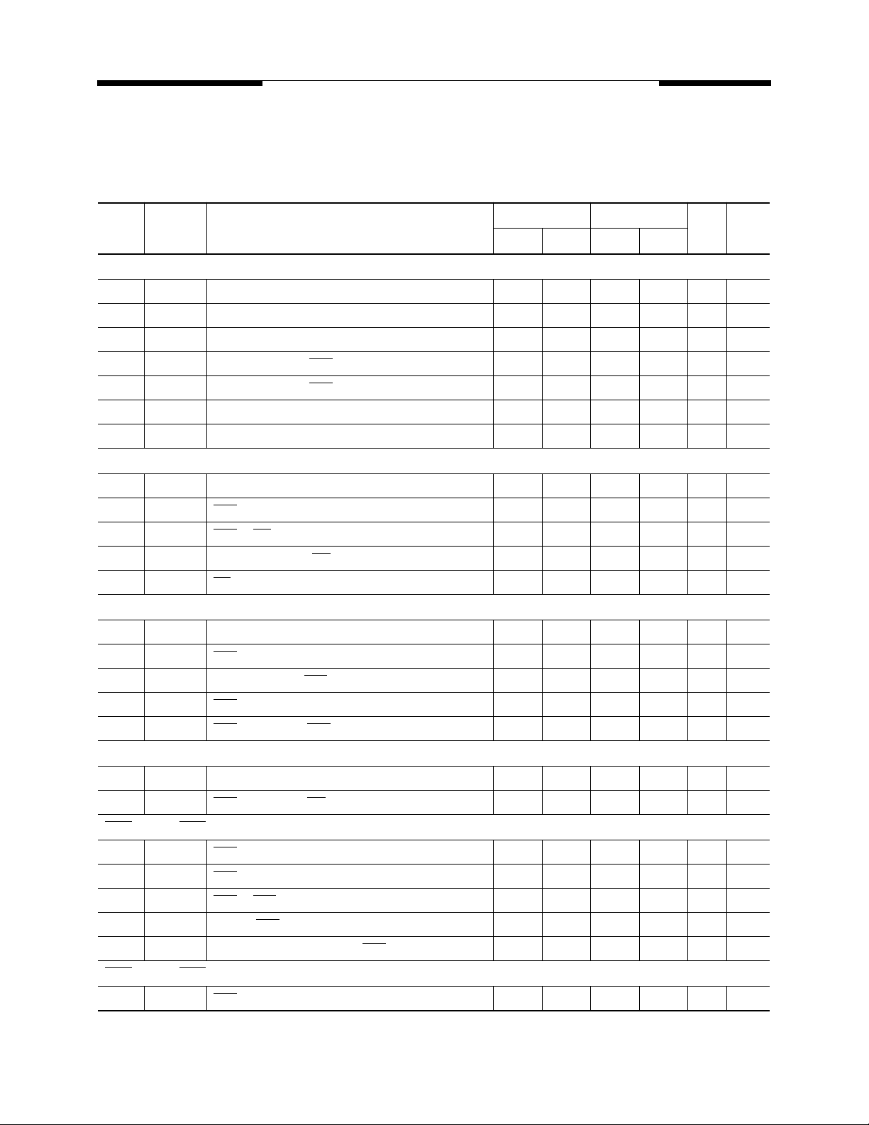
PIN CONFIGURATION
Top View
V
CC
I/O
I/O
WE
RAS
A
A
V
CC
1
2
1
3
2
4
5
6 21 A
11
10
A
9
0
A
10
1
A
11
2
A
12
3
13
26
25
24
23
22
19 A
18
17
16
15
14
311640002-02
V
SS
I/O
I/O
CAS
OE
9
8
A
7
A
6
A
5
A
4
V
SS
V53C516400A
Pin Names
A
–A
0
11
RAS
CAS Column Address Strobe
4
3
WE Write Enable
OE
–I/O
I/O
1
4
V
CC
V
SS
NC No Connect
Description Pkg. Pin Count
SOJ K 26/24
TSOP-II T 26/24
Row, Column Address Inputs
Row Address Strobe
Output Enable
Data Input, Output
5V Supply
0V Supply
V53C516400A Rev. 1.1 March 1998
2
MOSEL VITELIC
Absolute Maximum Ratings*
Operating temperature range ..................0 to 70 ° C
Storage temperature range ............... -55 to 150 ° C
Input/output voltage....-0.5 to min (V
Power supply voltage ..........................-1.0 to 4.6 V
Power dissipation .......................................... 1.0 W
Data out current (short circuit)...................... 50 mA
*Note: Operation above Absolute Maximum Ratings can
adversely affect device reliability.
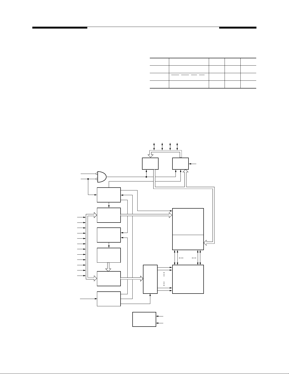
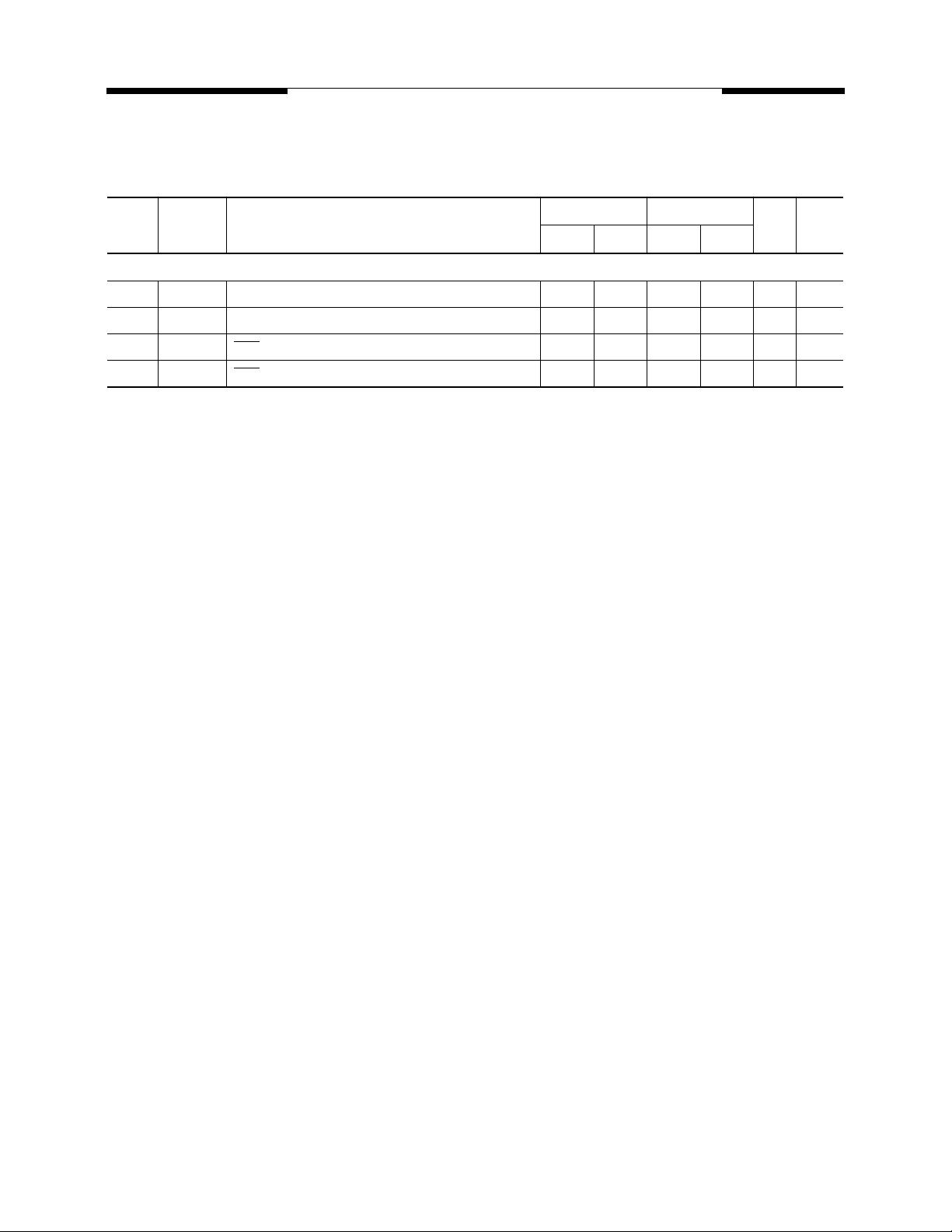
Block Diagram
WE
CAS
+0.5, 4.6) V
CC
4096 x 4
V53C516400A
Capacitance*
T
= 25 ° C, V
A
Symbol Parameter Typ. Max. Unit
C
IN1
C
IN2
C
OUT
*Note: Capacitance is sampled and not 100% tested.
I/O1 I/O2 I/O3I/O4
Data In
Buffer
4
= 5 V ± 10%, V
CC
Address Input — 5 pF
, CAS, WE, OE — 7 pF
RAS
Data Input/Output — 7 pF
Data Out
Buffer
OE
4
SS
= 0 V
A0
A1
A2
A3
A4
A5
A6
A7
A8
A9
A10
A11
RAS
No. 2 Clock
Generator
10
12 12
Column
Address
Buffers (10)
Refresh
Controller
Refresh
Counter (12)
12
Row
Address
Buffers (12)
No. 1 Clock
Generator
Voltage Down
Row
Decoder
Generator
10
4096
VCC
VCC (internal)
Column
Decoder
Sense Amplifier
I/O Gating
1024
x4
Memory Array
4096 x 1024 x 4
4
511640002-04
V53C516400A Rev. 1.1 March 1998
3
µ
≤
≤
µ
≤
≤
MOSEL VITELIC
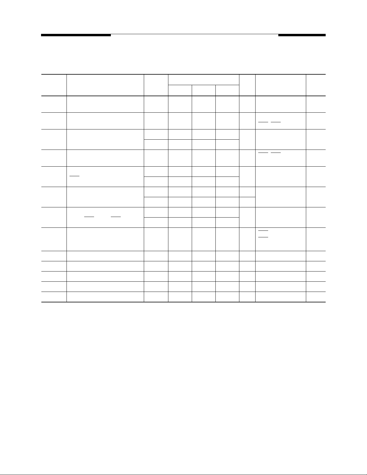
DC and Operating Characteristics
T
= 0 ° C to 70 ° C, V
A
Symbol Parameter
I
LI
I
LO
I
CC1
I
CC2
I
CC3
I
CC4
I
CC5
I
CC6
V
V
V
V
V
CC
IL
IH
OL
OH
Input Leakage Current
(any input pin)
Output Leakage Current
(for High-Z State)
V
Supply Current,
CC
Operating
V
Supply Current,
CC
TTL Standby
V
Supply Current,
CC
-Only Refresh
RAS
V
Supply Current,
CC
Fast Page Mode Operation
V
Supply Current,
CC
during CAS
V
Supply Current,
CC
CMOS Standby
Power Supply Voltage 4.5 5.0 5.5 V
Input Low Voltage –0.5 0.8 V 1
Input High Voltage 2.4 V
Output Low Voltage 0.4 V I
Output High Voltage 2.4 V I
= 5V ± 10%, V
CC
-before-RAS Refresh
= 0 V, unless otherwise specified.
SS
V53C516400A
(1-2)
Access
Time
50 50 mA t
60 40
50 50 mA t
60 40
50 25 mA Minimum Cycle 2, 3, 4
60 20
50 50 mA 2, 4
60 40
V53C516400A
–10 10
–10 10
1.0 mA RAS
CC
Unit Test Conditions NotesMin. Typ. Max.
A V
A V
2 mA RAS
+ 0.5 V 1
V
SS
SS
RAS
RC
other inputs ≥ V
RC
CAS
other input ≥ V
= 4.2 mA 1
OL
OH
V
IN
CC
V
V
OUT
, CAS at V
= t
RC
, CAS at V
= t
RC
≥ V
≥ V
CC
IH
(min.) 2, 3, 4
IH
SS
(min.) 2, 4
– 0.2 V,
CC
– 0.2 V
CC
SS
= –5 mA 1
1
1
1
V53C516400A Rev. 1.1 March 1998
4
MOSEL VITELIC
AC Characteristics
T
= 0 to 70 ˚C,V
A
# Symbol Parameter
Common Parameters
1 t
RC
2 t
RP
3 t
RAS
4 t
CAS
5 t
ASR
6 t
RAH
7 t
ASC
8 t
CAH
9 t
RCD
10 t
RAD
11 t
RSH
12 t
CSH
13 t
CRP
14 t
T
15 t
REF
Read Cycle
(5,6)
= 5V ± 10%, t
CC
Random read or write cycle time 90 – 110 – ns
precharge time 30 – 40 – ns
RAS
pulse width 50 10k 60 10k ns
RAS
pulse width 13 10k 15 10k ns
CAS
Row address setup time 0 – 0 – ns
Row address hold time 8 – 10 – ns
Column address setup time 0 – 0 – ns
Column address hold time 10 – 15 – ns
RAS to CAS delay time 18 37 20 45 ns
RAS to column address delay 13 25 15 30 ns
RAS hold time 13 15 – ns
CAS hold time 50 60 – ns
CAS to RAS precharge time 5 – 5 – ns
Transition time (rise and fall) 3 50 3 50 ns 7
Refresh period – 64 – 64 ms
= 2 ns
T
V53C516400A
-50 -60
Unit Notemin. max. min. max.
16 t
17 t
18 t
19 t
20 t
21 t
22 t
23 t
24 t
25 t
26 t
27 t
28 t
29 t
30 t
RAC
CAC
CAA
OEA
RAL
RCS
RCH
RRH
CLZ
OFF
OEZ
DZC
DZO
CDD
ODD
Access time from RAS – 50 – 60 ns 8, 9
Access time from CAS – 13 – 15 ns 8, 9
Access time from column address – 25 – 30 ns 8,10
OE access time – 13 – 15 ns
Column address to RAS lead time 25 – 30 – ns
Read command setup time 0 – 0 – ns
Read command hold time 0 – 0 – ns 11
Read command hold time referenced to RAS 0 – 0 – ns 11
CAS to output in low-Z 0 – 0 – ns 8
Output buffer turn-off delay 0 13 0 15 ns 12
Output turn-off delay from OE 0 13 0 15 ns 12
Data to CAS low delay 0 – 0 – ns 13
Data to OE low delay 0 – 0 – ns 13
CAS high to data delay 13 – 15 – ns 14
OE high to data delay 13 – 15 – ns 14
V53C516400A Rev. 1.1 March 1998
5
MOSEL VITELIC
V53C516400A
AC Characteristics
(5,6)
TA = 0 to 70 ˚C,VCC = 5V ±10%, tT = 2 ns
# Symbol Parameter
Write Cycle
31 t
WCH
32 t
WP
33 t
WCS
34 t
RWL
35 t
CWL
36 t
DS
37 t
DH
Read-modify-Write Cycle
38 t
RWC
39 t
RWD
40 t
CWD
41 t
AWD
42 t
OEH
Fast Page Mode Cycle
Write command hold time 8 – 10 – ns
Write command pulse width 8 – 10 – ns
Write command setup time 0 – 0 – ns 15
Write command to RAS lead time 13 – 15 – ns
Write command to CAS lead time 13 – 15 – ns
Data setup time 0 – 0 – ns 16
Data hold time 8 – 10 – ns 16
Read-write cycle time 126 – 150 – ns
RAS to WE delay time 68 – 80 – ns 15
CAS to WE delay time 31 – 35 – ns 15
Column address to WE delay time 43 – 50 – ns 15
OE command hold time 13 – 15 – ns
-50 -60
Unit Notemin. max. min. max.
43 t
44 t
45 t
46 t
47 t
PC
CP
CPA
RASP
RHPC
Fast Page mode cycle time 35 – 40 – ns
CAS precharge time 10 – 10 – ns
Access time from CAS precharge – 30 – 35 ns 7
RAS pulse width in Fast mode 50 200k 60 200k ns
CAS precharge to RAS Delay 30 – 35 – ns
Fast Page Mode Read-modify-Write Cycle
48 t
49 t
PRWC
CPWD
Fast Page mode read-write cycle time 71 – 80 – ns
CAS precharge to WE 48 – 55 – ns
CAS-before-RAS Refresh Cycle
50 t
51 t
52 t
53 t
54 t
CSR
CHR
RPC
WRP
WRH
CAS setup time 10 – 10 – ns
CAS hold time 10 – 10 – ns
RAS to CAS precharge time 5 – 5 – ns
Write to RAS precharge time 10 – 10 – ns
Write hold time referenced to RAS 10 – 10 – ns
CAS-before-RAS Counter Test Cycle
55 t
CPT
CAS precharge time 35 – 40 – ns
V53C516400A Rev. 1.1 March 1998
6
MOSEL VITELIC
V53C516400A
AC Characteristics
(5,6)
TA = 0 to 70 ˚C,VCC = 5V ±10%, tT = 2 ns
# Symbol Parameter
Test Mode
56 t
57 t
58 t
59 t
WTS
WTH
CHRT
RAHT
Write command setup time 10 – 10 – ns
Write command hold time 10 – 10 – ns
CAS hold time 30 – 30 – ns
RAS hold time in test mode 30 – 30 – ns
-50 -60
Unit Notemin. max. min. max.
V53C516400A Rev. 1.1 March 1998
7

MOSEL VITELIC
Notes:
1) All voltages are referenced to VSS.
V53C516400A
2) I
3) I
4) Address can be changed once or less while RAS
CC1
CC1
, I
CC3
and I
, I
and I
CC4
depend on output loading. Specified values are obtained with the output open.
CC4
depend on cycle rate.
CC5
= VIL. In case of I
it can be changed once or less during a Fast
CC4
Page mode cycle
5) An initial pause of 200 µs is required after power-up followed by 8 RAS
cycles of which at least one cycle has to be
a refresh cycle, before proper device operation is achieved. In case of using the internal refresh counter, a minimum
of 8 CAS
6) AC measurements assume t
7) V
between V
8) Measured with the specified current load and 100 pF at V
the latter of t
9) Operation within the t
only. If t
10) Operation within the t
only. If t
11) Either t
12) t
OFF (max.)
to output voltage levels. t
13) Either t
14) Either t
15) t
WCS
characteristics only. If t
(high impedance) through the entire cycle; if t
-before-RAS initialization cycles instead of 8 RAS cycles are required.
= 2 ns.
T
IH (min.)
, t
and V
and VIL.
IH
RAC
is greater than the specified t
RCD
is greater than the specified t
RAD
or t
RCH
, t
OEZ (max.)
or t
DZC
or t
CDD
, t
RWD
CWD
are reference levels for measuring timing of input signals. Transition times are also measured
IL (max.)
= 0.8 V and VOH = 2.0 V. Access time is determined by
, t
, t
CAC
CAA,tCPA
RCD (max.)
RAD (max.)
must be satisfied for a read cycle.
RRH
, t
. t
OEA
CAC
limit ensures that t
RCD (max.)
limit ensures that t
RAD (max.)
is measured from tristate.
OL
RAC (max.)
can be met. t
limit, then access time is controlled by t
RAC (max.)
can be met. t
limit, then access time is controlled by t
define the time at which the output achieves the open-circuit conditions and are not referenced
is referenced from the rising edge of RAS or CAS, whichever occurs last.
OFF
must be satisfied.
DZO
must be satisfied.
ODD
and t
are not restrictive operating parameters. They are included in the data sheet as electrical
AWD
WCS
> t
WCS (min.)
, the cycle is an early write cycle and data out pin will remain open-circuit
> t
RWD
RWD (min.)
, t
CWD
RCD (max.)
RAD (max.)
> t
CWD (min.)
is specified as a reference point
.
CAC
is specified as a reference point
.
CAA
and t
AWD
> t
AWD (min.)
is a read-write cycle and I/O will contain data read from the selected cells. If neither of the above sets of conditions
is satisfied, the condition of I/O (at access time) is indeterminate.
, the cycle
16) These parameters are referenced to the CAS
write cycles.
V53C516400A Rev. 1.1 March 1998
leading edge in early write cycles and to the WE leading edge in read-
8
 Loading...