

Mosel Vitelic V53C16256SH Datasheet
■
■
■
■
■
■
■
■
■
■
■
0 °
MOSEL VITELIC
V53C16256SH
PRELIMINARY
256K X 16 FAST PAGE MODE
CMOS DYNAMIC RAM WITH
SELF REFRESH
HIGH PERFORMANCE 40 50
Max. RAS
Max. Column Address Access Time, (t
Min. Fast Page Mode Cycle Time, (t
Min. Read/Write Cycle Time, (t
Access Time, (t
Features
256K x 16-bit organization
Fast Page Mode for a sustained data rate
of 43 MHz
RAS access time: 40, 50 ns
Dual CAS Inputs
Low power dissipation
Read-Modify-Write, RAS-Only Refresh,
CAS-Before-RAS Refresh, and Self Refresh
Refresh Interval: 512 cycles/8 ms
Available in 40-pin 400 mil SOJ and
40/44L-pin 400 mil TSOP-II packages
Single 5.0V ± 10% Power Supply
TTL Interface
Self Refresh: 512 cycles/8ms
) 40 ns 50 ns
RAC
) 20 ns 24 ns
CAA
) 23 ns 28 ns
PC
) 75 ns 90 ns
RC
Description
The V53C16256SH is a 262,144 x 16 bit highperformance CMOS dynamic random access memory. The V53C16256SH offers Fast Page mode
with dual CAS inputs. An address, CAS and RAS input capacitances are reduced to one quarter when
the x4 DRAM is used to construct the same memory
density. The V53C16256SH has symmetric address and accepts 512 cycle 8ms interval.
All inputs are TTL compatible. Fast Page Mode
operation allows random access up to 512 x 16 bits,
within a page, with cycle times as short as 23ns.
The V53C16256SH is best suited for graphics,
and DSP applications.
Device Usage Chart
Operating
Temperature
Range
C to 70 ° C • • • • • Blank
V53C16256SH Rev. 0.1 December 1998
Package Outline Access Time (ns) Power
K T 40 50 Std.
1
Temperature
Mark
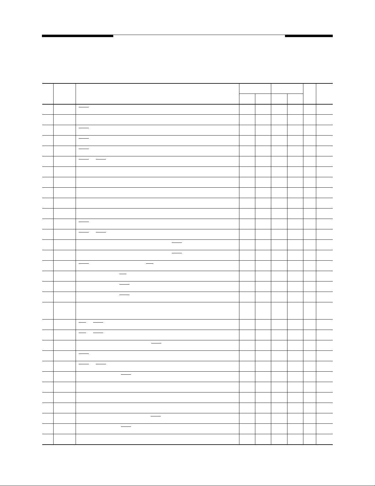
MOSEL VITELIC
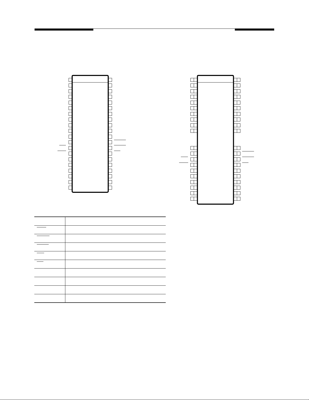
40-Pin Plastic SOJ
PIN CONFIGURATION
Top View
Vcc
I/O1
I/O2
I/O3
I/O4
Vcc
I/O5
I/O6
I/O7
I/O8
WE
RAS
Vcc
Pin Names
NC
NC
NC
A0
A1
A2
A3
1
2
3
4
5
6
7
8
9
10
11
12
13
14
15
16
17
18
19
20
40
39
38
37
36
35
34
33
32
31
30
29
28
27
26
25
24
23
22
21
16256L-02
Vss
I/O16
I/O15
I/O14
I/O13
Vss
I/O12
I/O11
I/O10
I/O9
NC
LCAS
UCAS
OE
A8
A7
A6
A5
A4
Vss
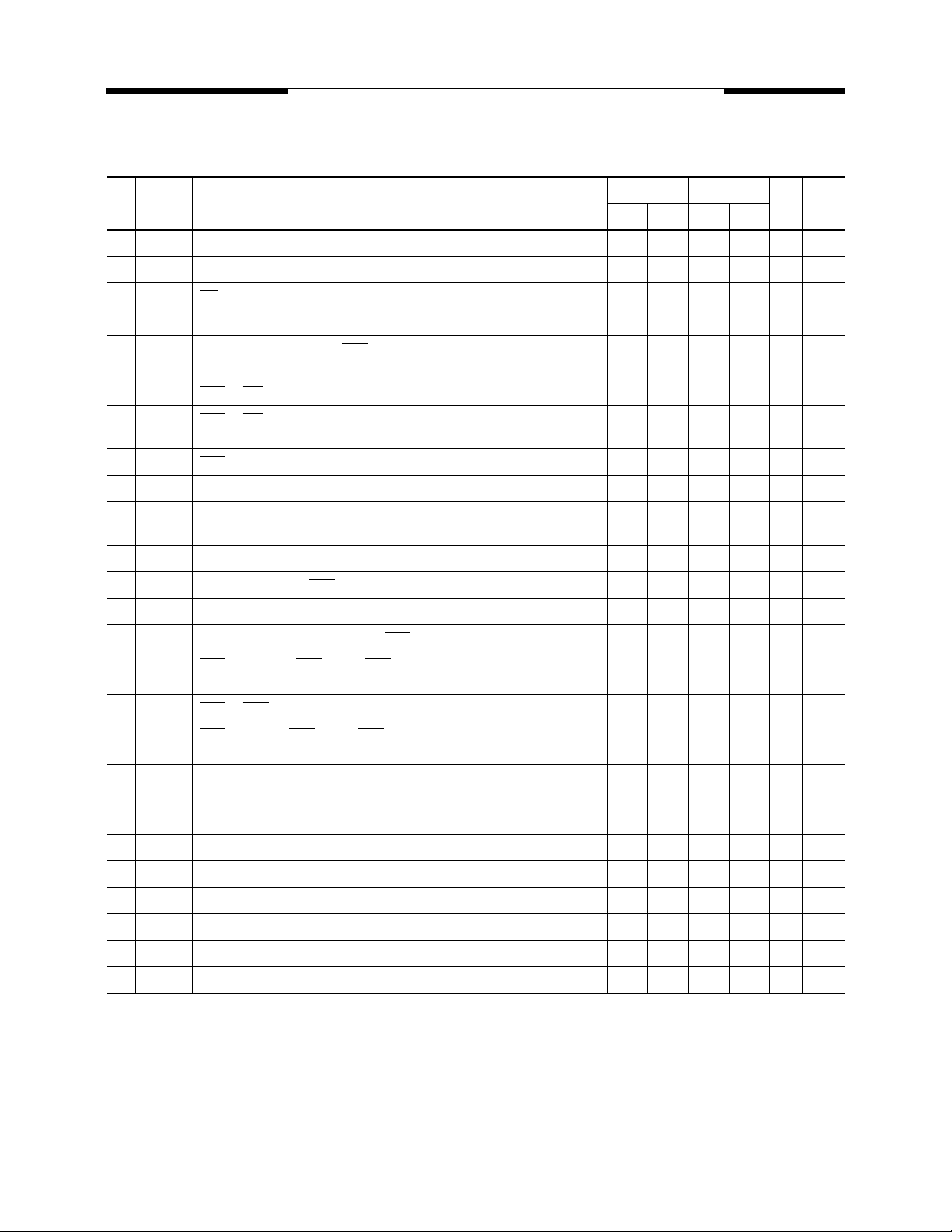
V53C16256SH
40/44 Pin Plastic TSOP-II
PIN CONFIGURATION
Top View
Vcc
I/O1
I/O2
I/O3
I/O4
Vcc
I/O5
I/O6
I/O7
I/O8
NC
NC
WE
RAS
NC
A0
A1
A2
A3
Vcc
1
2
3
4
5
6
7
8
9
10
13
14
15
16
17
18
19
20
21
22
44
43
42
41
40
39
38
37
36
35
32
31
30
29
28
27
26
25
24
23
16256L-03
Vss
I/O16
I/O15
I/O14
I/O13
Vss
I/O12
I/O11
I/O10
I/O9
NC
LCAS
UCAS
OE
A8
A7
A6
A5
A4
Vss
A
–A
0
RAS
UCAS
LCAS
WE
OE
–I/O
I/O
1
V
CC
V
SS
8
Address Inputs
Row Address Strobe
Column Address Strobe Upper Byte Control
Column Address Strobe Lower Byte Control
Write Enable
Output Enable
Data Input, Output
16
+3.3V Supply
0V Supply
NC No Connect
V53C16256SH Rev. 0.1 December 1998
2
MOSEL VITELIC
Absolute Maximum Ratings*
Ambient Temperature
Under Bias................................ –10 ° C to +80 ° C
Storage Temperature (plastic)..... –55 ° C to +125 ° C
Voltage Relative to V
Data Output Current .....................................50 mA
Power Dissipation..........................................1.0 W
*Note: Operation above Absolute Maximum Ratings can
adversely affect device reliability.
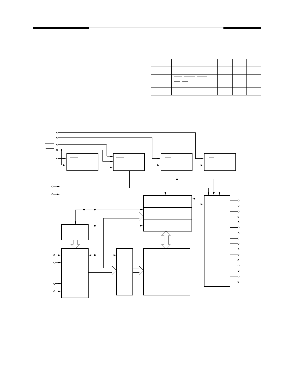
Block Diagram
OE
WE
UCAS
LCAS
RAS
RAS CLOCK
GENERATOR
.................–1.0 V to +7.0 V
SS
CAS CLOCK
GENERATOR
256K x 16
V53C16256SH
Capacitance*
T
= 25 ° C, V
A
Symbol Parameter Typ. Max. Unit
C
IN1
C
IN2
C
OUT
* Note: Capacitance is sampled and not 100% tested
WE CLOCK
GENERATOR
= 5.0 V ± 10%, V
CC
Address Input 3 4 pF
RAS
, UCAS, LCAS,
WE, OE
Data Input/Output 5 7 pF
= 0 V
SS
45pF
OE CLOCK
GENERATOR
V
CC
V
SS
I/O
DATA I/O BUS
COLUMN DECODERS
Y
-Y
8
0
SENSE AMPLIFIERS
REFRESH
COUNTER
512 x 16
9
A
0
A
1
•
•
•
A
7
A
8
ADDRESS BUFFERS
AND PREDECODERS
X0-X
8
512
MEMORY
ROW
ARRAY
DECODERS
I/O
BUFFER
16256L-04
I/O
I/O
I/O
I/O
I/O
I/O
I/O
I/O
I/O
I/O
I/O
I/O
I/O
I/O
I/O
1
2
3
4
5
6
7
8
9
10
11
12
13
14
15
16
V53C16256SH Rev. 0.1 December 1998
3
µ
≤
≤
µ
≤
≤
µ
MOSEL VITELIC
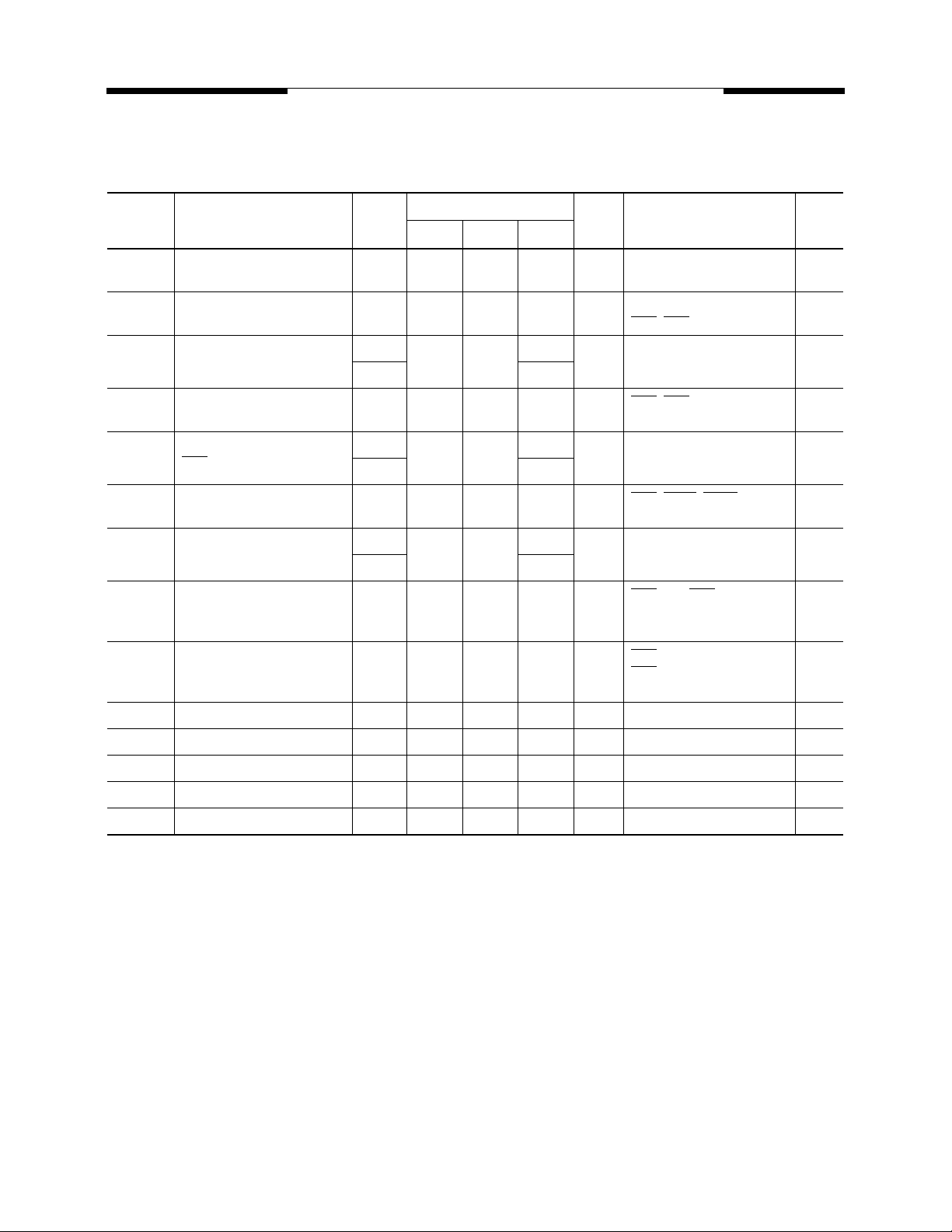
DC and Operating Characteristics
T
= 0 ° C to 70 ° C, V
A
Symbol Parameter
I
LI
I
LO
I
CC1
I
CC2
I
CC3
I
CCS
I
CC4
I
CC5
I
CC6
V
V
V
V
V
CC
IL
IH
OL
OH
Input Leakage Current
(any input pin)
Output Leakage Current
(for High-Z State)
V
Supply Current,
CC
Operating
V
Supply Current,
CC
TTL Standby
V
Supply Current,
CC
RAS
-Only Refresh
Self Refresh Current 400
V
Supply Current,
CC
Fast Page Mode Operation
V
Supply Current,
CC
Standby, Output Enabled
other inputs ≥ V
V
Supply Current,
CC
CMOS Standby
Supply Voltage 4.75 5.0 5.25 V
Input Low Voltage –1 0.8 V 3
Input High Voltage 2.0 V
Output Low Voltage 0.4 V I
Output High Voltage 2.4 V I
= 5V ± 5%, V
CC
SS
= 0 V, unless otherwise specified.
SS
Access
Time
40 180 mA t
50 160
40 180 mA t
50 160
40 170 mA Minimum Cycle 1, 2
50 150
(1-2)
V53C16256SH
–10 10
–10 10
V53C16256SH
Unit Test Conditions NotesMin. Typ. Max.
AV
AV
2 mA RAS
A RAS
2 mA RAS
1 mA RAS
+1 V 3
CC
V
SS
SS
RAS
= t
RC
other inputs ≥ V
= t
RC
V
IN
CC
V
V
OUT
, CAS at V
, CAS at V
CC
IH
(min.) 1, 2
RC
IH
SS
(min.) 2
RC
, LCAS, UCAS = 0.2V
, CAS
IH
CC
CC
CC
– 0.2 V,
– 0.2 V,
– 0.2V or 0.2V
=V
A0 – A8 = V
=V
≥ V
CAS
≥ V
All other inputs ≥ V
= 2.0 mA
OL
= –2.0 mA
OH
IL
SS
1
V53C16256SH Rev. 0.1 December 1998
4
MOSEL VITELIC
AC Characteristics
T
= 0 ° C to 70 ° C, V
A
AC Test conditions, input pulse levels 0 to 3V
# Symbol Parameter
1t
2t
3t
4t
5t
6t
7t
8t
9t
10 t
11 t
12 t
13 t
14 t
15 t
16 t
17 t
18 t
19 t
20 t
21 t
22 t
23 t
24 t
25 t
26 t
27 t
28 t
29 t
30 t
31 t
32 t
RAS
RC
RP
CSH
CAS
RCD
RCS
ASR
RAH
ASC
CAH
RSH (R)
CRP
RCH
RRH
ROH
OAC
CAC
RAC
CAA
LZ
HZ
AR
RAD
RSH (W)
CWL
WCS
WCH
WP
WCR
RWL
DS
RAS Pulse Width 40 75 50 75K ns
Read or Write Cycle Time 75 90 ns
RAS Precharge Time 25 30 ns
CAS Hold Time 40 50 ns
CAS Pulse Width 12 14 ns
RAS to CAS Delay 17 28 19 36 ns
Read Command Setup Time 0 0 ns 4
Row Address Setup Time 0 0 ns
Row Address Hold Time 7 9 ns
Column Address Setup Time 0 0 ns
Column Address Hold Time 5 7 ns
RAS Hold Time (Read Cycle) 12 14 ns
CAS to RAS Precharge Time 5 5 ns
Read Command Hold Time Referenced to CAS 0 0 ns 5
Read Command Hold Time Referenced to RAS 0 0 ns 5
RAS Hold Time Referenced to OE 810ns
Access Time from OE 12 14 ns
Access Time from CAS 12 14 ns 6, 7
Access Time from RAS 45 55 ns 6, 8, 9
Access Time from Column
Address
OE or CAS to Low-Z Output 0 0 ns 16
OE or CAS to High-Z Output 0608ns16
Column Address Hold Time from RAS 30 40 ns
RAS to Column Address Delay Time 12 20 14 26 ns 11
RAS or CAS Hold Time in Write Cycle 12 14 ns
Write Command to CAS Lead Time 12 14 ns
Write Command Setup Time 0 0 ns 12, 13
Write Command Hold Time 5 7 ns
Write Pulse Width 5 7 ns
Write Command Hold Time from RAS 30 40 ns
Write Command to RAS Lead Time 12 14 ns
Data in Setup Time 0 0 ns 14
= 5V ± 10%, V
CC
= 0V unless otherwise noted
SS
V53C16256SH
40 50
Unit NotesMin. Max. Min. Max.
20 24 ns 6, 7, 10
V53C16256SH Rev. 0.1 December 1998
5
MOSEL VITELIC
V53C16256SH
AC Characteristics
# Symbol Parameter
33 t
34 t
35 t
36 t
37 t
38 t
39 t
40 t
41 t
42 t
43 t
44 t
45 t
46 t
47 t
DH
WOH
OED
RWC
RRW
CWD
RWD
CRW
AWD
PC
CP
CAR
CAP
DHR
CSR
Data in Hold Time 5 7 ns 14
Write to OE Hold Time 6 8 ns 14
OE to Data Delay Time 6 8 ns 14
Read-Modify-Write Cycle Time 110 130 ns
Read-Modify-Write Cycle RAS Pulse
Width
CAS to WE Delay 30 34 ns 12
RAS to WE Delay in Read-Modify-Write
Cycle
CAS Pulse Width (RMW) 48 52 ns
Col. Address to WE Delay 38 42 ns 12
Fast Page Mode Read or Write Cycle
Time
CAS Precharge Time 5 7 ns
Column Address to RAS Setup Time 20 24 ns
Access Time from Column Precharge 22 27 ns 7
Data in Hold Time Referenced to RAS 30 40 ns
CAS Setup Time CAS-before-RAS
Refresh
(Cont’d)
40 50
Unit NotesMin. Max. Min. Max.
75 87 ns
58 68 ns 12
23 28 ns
10 10 ns
48 t
49 t
50 t
51 t
52 t
53 t
54 t
55 t
56 t
57 t
RPC
CHR
PCM
T
REF
REF
RASS
RPS
CHS
CHD
RAS to CAS Precharge Time 0 0 ns
CAS Hold Time CAS-before-RAS
812ns
Refresh
Fast Page Mode Read-Modify-Write
60 70 ns
Cycle Time
Transition Time (Rise and Fall) 3 50 3 50 ns 15
Refresh Interval (512 Cycles) 8 8 ms 17
Self Refresh 8 8 ms
RAS Pulse Width During Self Refresh 100 100 µs18
RAS Precharge Time During Self Refresh 100 100 ns 18
CAS Hold Time Width During Self Refresh 100 100 ns 18
CAS Low Time During Self Refresh 100 100 ns 18
V53C16256SH Rev. 0.1 December 1998
6
 Loading...