

Mosel Vitelic V436664S24VXTG-75PC, V436664S24VXTG-75, V436664S24VXTG-10PC Datasheet
MOSEL VITELIC
V436664S24V
3.3 VOLT 64M x 64 HIGH PERFORMANCE
UNBUFFERED SDRAM MODULE
PRELIMINARY
Features
■ 168 Pin Unbuffered 67,108,864 x 64 bit
Oganization SDRAM Modules
■ Utilizes High Performance 32M x 8 SDRAM in
TSOPII-54 Packages
■ Fully PC Board Layout Compatible to INTEL’S
Rev 1.0 Module Specification
■ Single +3.3V (± 0.3V) Power Supply
■ Programmable CAS
Wrap Sequence (Sequential & Interleave)
■ Auto Refresh (CBR) and Self Refresh
■ All Inputs, Outputs are LVTTL Compatible
■ 8192 Refresh Cycles every 64 ms
■ Serial Present Detect (SPD)
Part Number
V436664S24VXTG-75PC -75PC, CL=2,3
V436664S24VXTG-75 -75, CL=3
V436664S24VXTG-10PC -10PC, CL=2,3
Latency, Burst Length, and
Speed
Grade Configuration
64M x 64
(133 MHz)
64M x 64
(133 MHz)
64M x 64
(100 MHz)
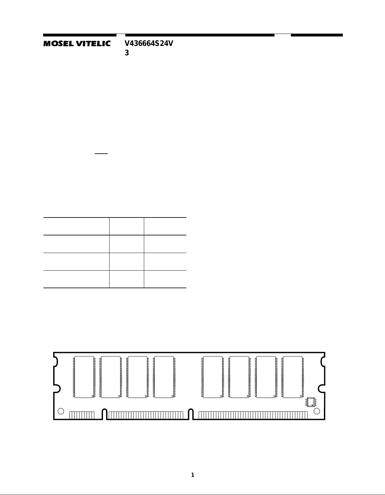
Description
The V436664S24V memory module is organized
67,108,864 x 64 bits in a 168 pin dual in line memory module (DIMM). The 64M x 64 unbuffered
DIMM uses 16 Mosel-Vitelic 32M x 8 SDRAM. The
x64 modules are ideal for use in high performance
computer systems where increased memory density and fast access times are required.
V436664S24V Rev. 1.1 March 2002
1
MOSEL VITELIC
V436664S24V
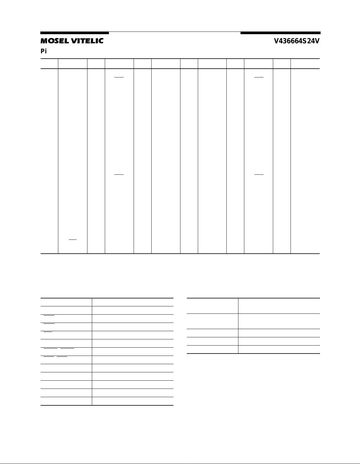
Pin Configurations (Front Side/Back Side)
Pin Front Pin Front Pin Front Pin Back Pin Back Pin Back
DQM5
CS1
RAS
VSS
A1
A3
A5
A7
A9
BA0
A11
VCC
CLK1
A12
VSS
CKE0
CS3
DQM6
DQM7
DU
VCC
NC
NC
CB6*
CB7*
VSS
I/O49
I/O50
141
142
143
144
145
146
147
148
149
150
151
152
153
154
155
156
157
158
159
160
161
162
163
164
165
166
167
168
10
11
12
13
14
15
16
17
18
19
20
21
22
23
24
25
26
27
28
1
2
3
4
5
6
7
8
9
VSS
I/O1
I/O2
I/O3
I/O4
VCC
I/O5
I/O6
I/O7
I/O8
I/O9
VSS
I/O10
I/O11
I/O12
I/O13
I/O14
VCC
I/O15
I/O16
CBO*
CB1*
VSS
NC
NC
VCC
WE
DQM0
29
30
31
32
33
34
35
36
37
38
39
40
41
42
43
44
45
46
47
48
49
50
51
52
53
54
55
56
DQM1
CS0
DU
VSS
A0
A2
A4
A6
A8
A10(AP)
BA1
VCC
VCC
CLK0
VSS
DU
CS2
DQM2
DQM3
DU
VCC
NC
NC
CB2*
CB3*
VSS
I/O17
I/O18
57
58
59
60
61
62
63
64
65
66
67
68
69
70
71
72
73
74
75
76
77
78
79
80
81
82
83
84
I/O19
I/O20
VCC
I/O21
NC
DU
CKE1
VSS
I/O22
I/O23
I/O24
VSS
I/O25
I/O26
I/O27
I/O28
VCC
I/O29
I/O30
I/O31
I/O32
VSS
CLK2
NC
WP
SDA
SCL
VCC
85
86
87
88
89
90
91
92
93
94
95
96
97
98
99
100
101
102
103
104
105
106
107
108
109
110
111
112
VSS
I/O33
I/O34
I/O35
I/O36
VCC
I/O37
I/O38
I/O39
I/O40
I/O41
VSS
I/O42
I/O43
I/O44
I/O45
I/O46
VCC
I/O47
I/O48
CB4*
CB5*
VSS
NC
NC
VCC
CAS
DQM4
113
114
115
116
117
118
119
120
121
122
123
124
125
126
127
128
129
130
131
132
133
134
135
136
137
138
139
140
I/O51
I/O52
VCC
I/O53
NC
DU
NC
VSS
I/O54
I/O55
I/O56
VSS
I/O57
I/O58
I/O59
I/O60
VCC
I/O61
I/O62
I/O63
I/O64
VSS
CLK3
NC
SA0
SA1
SA2
VCC
Notes:
* These pins ar e not used in this module.
Pin Names
A0–A12 Address Inputs
I/O1–I/O64 Data Inputs/Ou tputs
RAS
CAS
WE
BA0, BA1 Bank Selects
, CKE1 Clock Enable
CKE0
0–CS3 Chip Select
CS
CLK0–CLK3 Clock Input
DQM0–DQM7 Data Mask
VCC Power (+3.3 Volts)
VSS Ground
SCL Clock for Presence Detect
Row Address Strobe
Column Address Strobe
Read/Write Input
SDA Serial Data OUT for Presence
Detect
SA0–A2 Serial Data IN fo r P re s en c e
Detect
CB0–CB7 Check Bits (x72 Organization)
NC No Connection
DU Don’t Use
V436664S24V Rev. 1.1 March 2002
2
MOSEL VITELIC
I
I
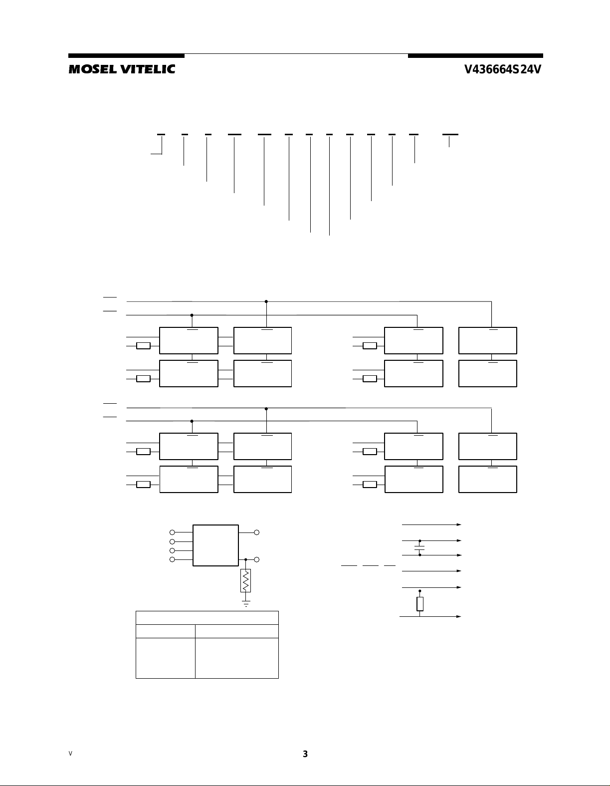
Module Part Number Information
V 4 3 66 64 S 2 4 V X T G - XX
MOSEL VITELIC
MANUFACTURED
SDRAM
3.3V
WIDTH
168 PIN Unbuffered
DIMM X8 COMPONENT
Block Diagram
CS1
CS0
DEPTH
REFRESH
RATE 8K
4 BANKS
LEAD FINISH
G = GOLD
COMPONENT
PACKAG E, T = TSOP
COMPONENT A=0.17u B=0.14u
REV LEVEL
LVTTL
V436664S24V
SPEED
75PC = PC133 CL3,2
75 = PC133 CL3
10PC = PC133 CL3,2
DQM0
I/O1–I/O8
DQM1
I/O9–I/O16
10Ω
10Ω
CS
DQM
I/O1–I/O8
CS
DQM
I/O1–I/O8
D0
D1
CS
DQM
I/O1–I/O8
CS
DQM
I/O1–I/O8
D8
D9
DQM4
I/O33–I/O40
DQM5
I/O41–I/O48
10Ω
10Ω
CS
DQM
I/O1–I/O8
DQM
I/O1–I/O8
D4
D5
CS
DQM
I/O1–I/O8
CSCS
DQM
I/O1–I/O8
D12
D13
CS3
CS2
DQM2
/O17–I/O24
CS
DQM
I/O1–I/O8
D2
10Ω
DQM3
/O25–I/O32
10Ω
2
E
PROM SPD (256 WORD X 8 BIT)
SA0
SA1
SA2
SCL
CS
DQM
I/O1–I/O8
SA0
SA1
SA2
SCL
D3
SDA
WP
CS
DQM
I/O1–I/O8
CS
DQM
I/O1–I/O8
47K
D10
D11
DQM6
I/O49–I/O56
DQM7
I/O57–I/O64
A12-A0, BA0, BA1
10Ω
10Ω
V
DD
V
SS
RAS, CAS, WE
CKE0
CS
DQM
I/O1–I/O8
CS
DQM
I/O1–I/O8
D6
D7
C0-C31
V
CC
DQM
I/O1–I/O8
DQM
I/O1–I/O8
D0-D15
D0-D15
,C32-C42
D0-D7
D0-D15
D0-D7
CS
D14
CS
D15
10K
CLOCK WIRING
CKE1
D9-D15
16M X 64
CLK0 4 SDRAM +3.3pF
CLK1 4 SDRAM +3.3pF
CLK2 4 SDRAM +3.3pF
CLK3 4 SDRAM +3.3pF
V436664S24V Rev. 1.1 March 2002
3
MOSEL VITELIC
V436664S24V
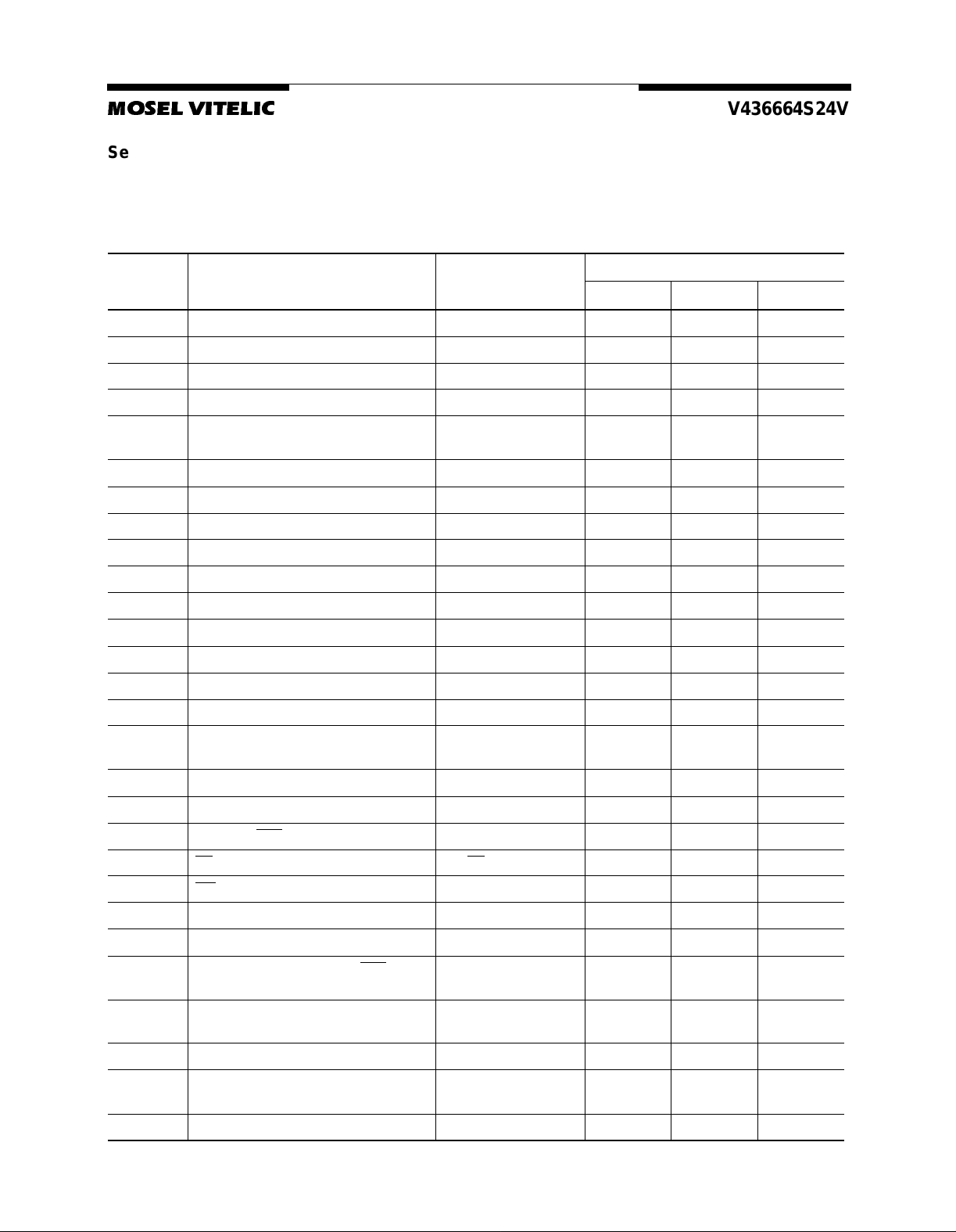
Serial Pr esence Detect Inf o rm ation
A serial presence detect storage device –
2
E
PROM – is assembled onto the module. Informa-
tion about the module configuration, speed, etc. is
written into the E
duction using a serial presence detect protocol (I
synchronous 2-wire bus)
2
PROM device during module pro-
SPD-Table :
Byte Num-
ber Function Described SPD Entry Value
0 Number of SPD bytes 128 80 80 80
1 Total bytes in Serial PD 256 08 08 08
2 Memory Type SDRAM 04 04 04
3 Number of Row Addresses (without BS bits) 13 0D 0D 0D
4 Number of Column Addresses (for x8
SDRAM)
5 Number of DIMM Banks 2 02 02 02
6 Module Data Width 64 40 40 40
7 Module Data Width (continued) 0 00 00 00
8 Module I nterface Levels LVTTL 01 01 01
9 SDRAM Cycle Time at CL=3 7.5 ns/10.0 ns 75 75 A0
10 SDRAM Access Time from Clock at CL=3 5.4 ns/6.0 ns 54 54 60
10 0A 0A 09
-75PC -75 -10PC
Hex Value
2
C
11 Dimm Config (Error Det/Corr.) none 00 00 00
12 Refresh Rate/Type Self-Refresh, 7.8µs82 82 82
13 SDRAM width, Primary x8 08 08 08
14 Error Checking SDRAM Data Width n/a / x8 00 00 00
15 Minimum Clock Delay from Back to Back
Random Column Address
16 Burst Length Support ed 1, 2, 4, 8 0F 0F 0F
17 Number of SDRAM Banks 4 04 04 04
18 Supported CAS
19 CS
20 WE
21 SDRAM DIMM Module Attributes Non Buffered/Non Reg. 00 00 00
22 SDRAM Device Attributes: General Vcc tol ± 10% 0E 0E 0E
23 Minimum Clock Cycle Time at CAS
24 Maximum Da ta A ccess T i me fr om C lock fo r
25 Minimum Clock Cycle Time at CL = 1 Not Supported 00 00 00
26 Maximum Data Access Time from Clock at
Latencies CS Latency = 0 01 01 01
Latencies WL = 0 01 01 01
= 2
CL = 2
CL = 1
Latencies CL = 3, 2 06 06 06
Latenc y
t
= 1 CLK 01 01 01
ccd
7.5ns/10.0 ns 75 A0 A0
5.4ns/6.0 ns 54 60 60
Not Supported 00 00 00
27 Minimum Row Precharge Ti me 15 ns/20 ns 0F 14 14
V436664S24V Rev. 1.1 March 2002
4
 Loading...