

Mosel Vitelic V436516Y04VATG-75PC, V436516Y04VATG-75, V436516Y04VATG-10PC Datasheet
MOSEL VITELIC
V436516Y04V
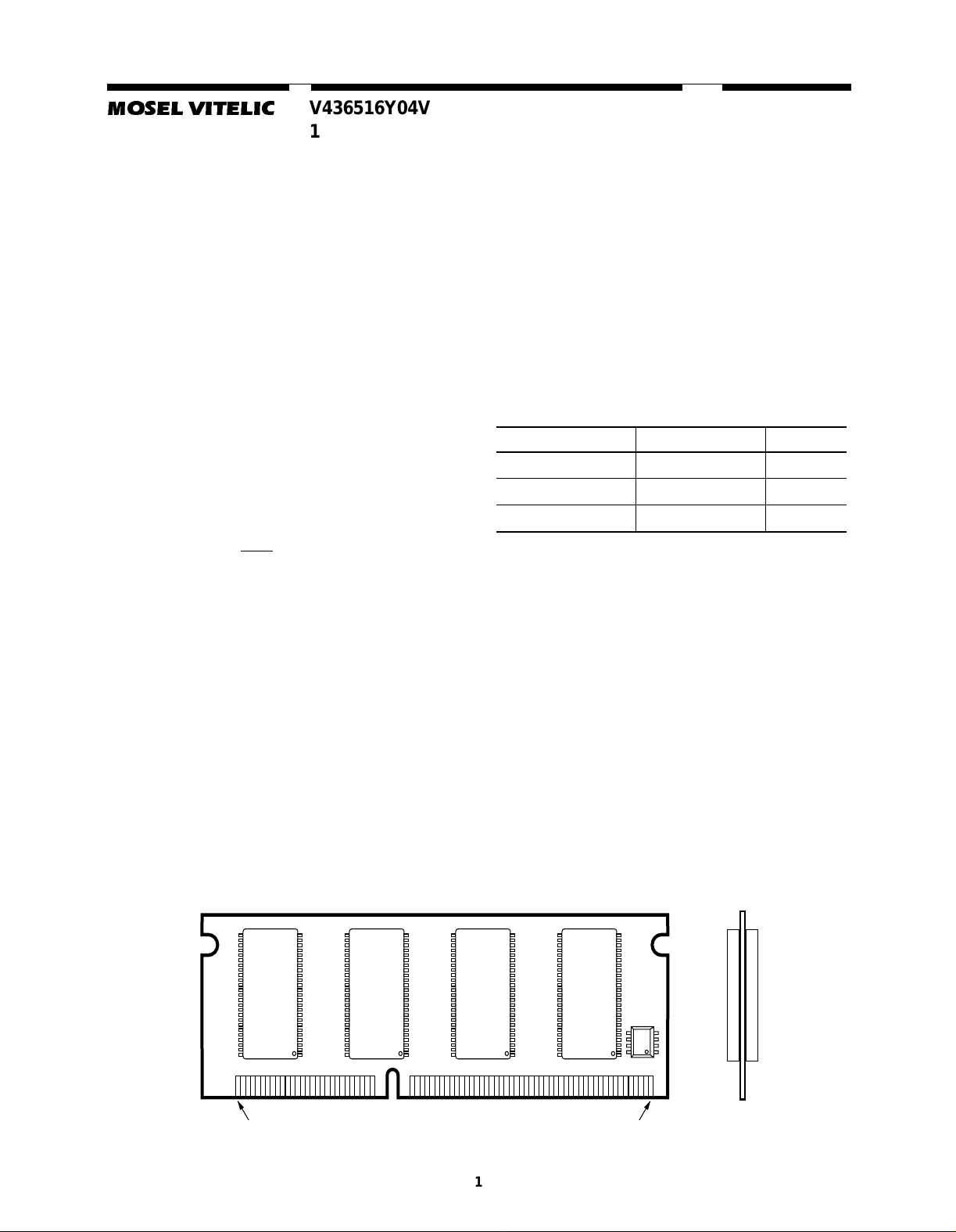
128MB 144-PIN UNBUFFERED SDRAM
SODIMM, 16MX64 3.3VOLT
PRELIMINARY
Features
■ JEDEC-standard144 pin, Small-Outline, Dual in
line Memory Module (SODI MM)
■ Serial Presen ce Det ec t with E
■ Nonbuffered
■ Fully Sync hronous , All Signals Registered on
Positive Edge of System Clock
■ Single +3.3V (± 0. 3V) Power Supply
■ All Device P ins are LVTT L Compatible
■ 4096 Ref res h Cy cles every 64 ms
■ Self-Refresh Mode
■ Internal Pipelined Operation; Column A ddres s
can be changed every System Clock
■ Programmable Burst Lengths: 1 , 2, 4, or 8
■ AutoPrecharge and Prechargeall Banks by A10
■ Data Mask Function by DQ M
■ Mode Re giste r S et Programming
■ Programmable ( CA S
Latency: 2, 3 Clocks)
■ SDRAM Performance
2
PROM
Description
The V43651 6Y04V memory module is organized
16,777,216 x 64 bits in a 144 pin S ODIMM. The
16M x 64 memory module uses 8 Mosel-Vitelic 8M
x 16 SDR AM. The x64 modules ar e ideal for use in
high performance computer systems where
increased memory density and fast access times
are required.
Part Number Speed Grade Configuration
V436516Y04VATG-75PC -75PC,CL=2,3(133MHZ)
V436516Y04VATG-75 -75, CL=3 (133MHZ)
V436516Y04VATG-10PC -10PC,CL=2,3(100MHZ)
16Mx64
16Mx64
16Mx64
8M x 16 8M x 16 8M x 16 8M x 16
1
Pin 2 on Backside
V436516Y04V Rev.1.0 October2001
59 61 143
Pin 144 on Backside
1
MOSEL VITELIC
V436516Y04V
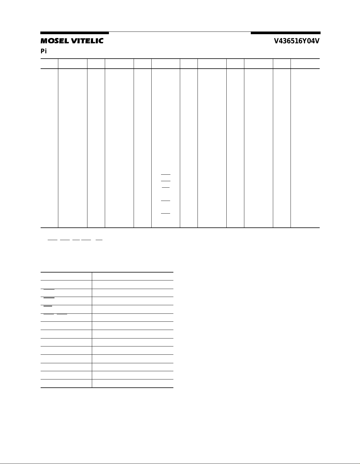
Pin Configurations (Front Side/Back Side)
Pin Front Pin Front Pin Front Pin Back Pin Back Pin Back
49
50
51
52
53
54
55
56
57
58
59
60
61
62
63
64
65
66
67
68
69
70
71
72
10
11
12
13
14
15
16
17
18
19
20
21
22
23
24
DQMB1
1
2
3
4
5
6
7
8
9
VSS
VSS
DQ0
DQ32
DQ1
DQ33
DQ2
DQ34
DQ3
DQ35
VDD
VDD
DQ4
DQ36
DQ5
DQ37
DQ6
DQ38
DQ7
DQ39
VSS
VSS
DQMB0
DQMB4
25
26
27
28
29
30
31
32
33
34
35
36
37
38
39
40
41
42
43
44
45
46
47
48
DQMB5
VDD
VDD
A0
A3
A1
A4
A2
A5
VSS
VSS
DQ8
DQ40
DQ9
DQ41
DQ10
DQ42
DQ11
DQ43
VDD
VDD
DQ12
DQ44
Note:
1. RAS,CAS,WECASx, CSx are active low signals.
DQ13
DQ45
DQ14
DQ46
DQ15
DQ47
VSS
VSS
NC
NC
NC
NC
CLK0
CKE0
VDD
VDD
RAS
CAS
WE
CKE1
CS0
NC
CS1
NC
73
74
75
76
77
78
79
80
81
82
83
84
85
86
87
88
89
90
91
92
93
94
95
96
NC
CLK1
VSS
VSS
NC
NC
NC
NC
VDD
VDD
DQ16
DQ48
DQ17
DQ49
DQ18
DQ50
DQ19
DQ51
VSS
VSS
DQ20
DQ52
DQ21
DQ53
97
98
99
100
101
102
103
104
105
106
107
108
109
110
111
112
113
114
115
116
117
118
119
120
DQ22
DQ54
DQ23
DQ55
VDD
VDD
A6
A7
A8
BA0
VSS
VSS
A9
BA1
A10
A11
VDD
VDD
DQMB2
DQMB6
DQMB3
DQMB7
VSS
VSS
121
122
123
124
125
126
127
128
129
130
131
132
133
134
135
136
137
138
139
140
141
142
143
144
DQ24
DQ56
DQ25
DQ57
DQ26
DQ58
DQ27
DQ59
VDD
VDD
DQ28
DQ60
DQ29
DQ61
DQ30
DQ62
DQ31
DQ63
VSS
VSS
SDA
SCL
VDD
VDD
Pin Names
A0–A11, BA0, BA1 Address, Bank Select
DQ0–DQ63 Data Inputs/Outputs
RAS
CAS
WE
0,CS1 Chip Select
CS
DQMB0–DQMB7 Output Enable
CKE0, CKE1 Clock Enable
CLK0–CLK1 Clock
SDA Serial Input/Output
SCL Serial Clock
VDD Power Supply
VSS Ground
NC No Connect (Open)
Row Address Strobes
Column Address Strobes
Write Enable
V436516Y04V Rev.1.0 October 2001
2
MOSEL VITELIC
Part Number Information
V436516Y04V
MOSEL VITELIC
MANUFACTURED
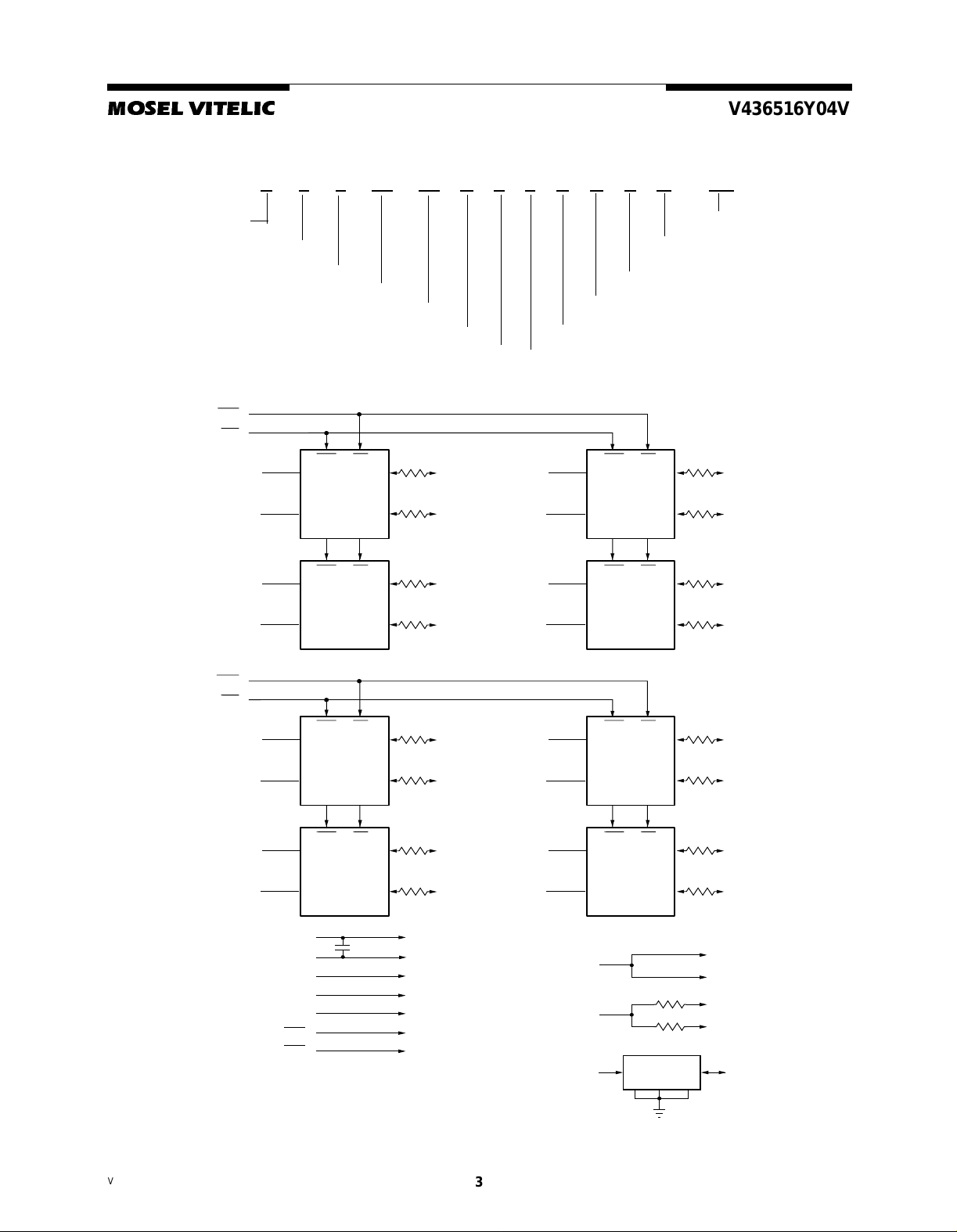
Block Diagram
DQMB0
DQMB1
DQMB2
DQMB3
V 4 3 65 16 Y 0 4 V A T G -XX
SDRAM
CS0
WE
3.3V
WIDTH
DEPTH
168 PIN REGISTERED
DIMM X16COMPONENT
REFRESH
RATE4K
CSWE CSWE
UDQM
U0
LDQM
CSWE CSWE
UDQM
U1
LDQM
DQ0–7
DQ8–15
DQ16–23
DQ24–31
DQMB4
DQMB5
DQMB6
DQMB7
LVTTL
4BANKS
COMPONENT
PACKAGE, T = TSOP
COMPONENT
REV LEVEL
UDQM
U2
LDQM
UDQM
U3
LDQM
LEAD FINISH
G=GOLD
SPEED
75 = PC133 CL3
75PC=PC133 CL2,3
10PC=PC100 CL2,3
DQ32–39
DQ40–47
DQ43–54
DQ55–63
CS1
WE
DQMB0
DQMB1
DQMB2
DQMB3
V
V
A0–A11, BA0, BA1
CKE0
CKEI
RAS
CAS
Note: All resistors are 10 Ohms
WE CSWE
CS
UDQM
U4
LDQM
CSWE CSWE
UDQM
U5
LDQM
DD
SS
U0–U7
U0–U7
U0–U3
U4–U7
U0–U7
U0–U7
DQ0–7
DQ8–15
DQ16–23
DQ24–31
DQMB4
DQMB5
DQMB6
DQMB7
UDQM
U6
LDQM
UDQM
U7
LDQM
CLK0
0Ω
CLKI
SCL SDA
0Ω
SPD
A0 A1 A2
DQ32–39
DQ40–47
DQ43–54
DQ55–63
U0, U1
U2, U3
U4, U5
U6, U7
V436516Y04V Rev.1.0 October 2001
3
MOSEL VITELIC
V436516Y04V
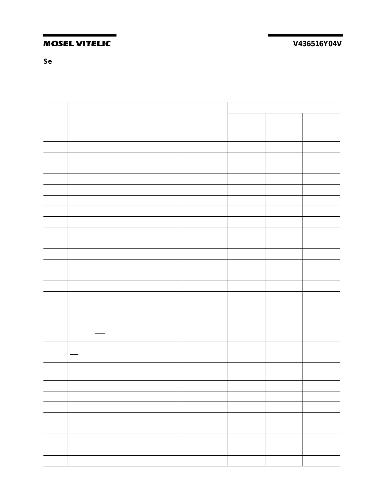
Serial Presence Detect Information
A serial presence detec t st orage device –
2
E
PROM – is assembled onto the module. Informa-
tion about the module configuration, s peed, etc. is
writtenintotheE
duction using a serial presence detect protocol (I
synchronous 2-wire bus)
2
PROM device during module pro-
SPD-Table for -75 modules:
Hex Value
Byte
Number Function Described SPD Entry Value
0 Numberof SPD bytes 128 80 80 80 1 Totalbytes in Serial PD 256 08 08 08 2 Memory Type SDRAM 04 04 04 3 Numberof Row Addresses(withoutBS bits) 12 0C 0C 0C 4 Number of Column Addresses (for x16 SDRAM) 9 09 09 09 5 Number of DIMM Banks 2 02 02 02 6 Module Data Width 64 40 40 40 7 Module Data Width(continued) 0 00 00 00 8 Module Interface Levels LVTTL 01 01 01 9 SDRAMCycleTimeatCL=3 7.5ns/10.0ns 75 75 A0
10 SDRAM Access Time from Clock at CL=3 5.4 ns/6.0 ns 54 54 60
133 MHz
-75PC
133 MHZ
-75
100 MHZ
-10PC
2
C
11 Dimm Config (Error Det/Corr.) none 00 00 00 12 Refresh Rate/Type Self-Refresh, 15.6µs80 80 80 13 SDRAM width, Primary x16 10 10 10 14 ErrorCheckingSDRAM Data Width n/a / x8 00 00 00 15 Minimum Clock Delay from Back to Back
RandomColumn Address 16 Burst Length Supported 1, 2, 4, 8 0F 0F 0F 17 Number of SDRAM Banks 4 04 04 04 18 Supported CAS 19 CS 20 WE 21 SDRAM DIMM Module Attributes Non Buffered/Non
22 SDRAM Device A ttributes: General Vcc tol ± 10% 0E 0E 0E 23 Minimum Clock Cycle Time at CAS 24 Maximum Data AccessTimefromClockfor CL = 2 5.4 ns/6.0ns 54 60 60 25 Minimum Clock Cycle TimeatCL = 1 Not Supported 00 00 00 26 Maximum Data Access Time from Clock at CL = 1 Not Supported 00 00 00
Latencies CS Latency = 0 01 01 01
Latencies WL = 0 01 01 01
Latencies CL = 2 & 3 06 06 06
Latency = 2 7.5ns/10.0ns 75 A0 A0
t
=1CLK 01 01 01
ccd
00 00 00
Reg.
27 Minimum Row Precharge Time t
28 Minimum Row Active to Row Active Delay t
29 Minimum RAS to CAS
V436516Y04V Rev.1.0 October 2001
Delay t
RP
RCD
RRD
15 ns/20 ns 0F 14 14 14 ns/15 ns 0E 0F 0F 15 ns/20 ns 0F 14 14
4
 Loading...