


Mosel Vitelic V29C51000T-90T, V29C51000T-90P, V29C51000T-90J, V29C51000T-70T, V29C51000T-70P Datasheet
...
MOSEL VITELIC
1
V29C51000T/V29C51000B
512K BIT (65,536 x 8 BIT)
5 VOLT CMOS FLASH MEMORY
PRELIMINARY
V29C51000T/V29C51000B Rev. 0.5 October 2000
Features
■
64Kx8-bit Organization
■
Address Access Time: 45, 70, 90 ns
■
Single 5V ± 10% Power Supply
■
Sector Erase Mode Operation
■
8KB Boot Block (lockable)
■
512 bytes per Sector, 128 Sectors
– Sector-Erase Cycle Time: 10ms (Max)
– Byte-Program Cycle Time: 20 µ s (Max)
■
Minimum 10,000 Erase-Program Cycles
■
Low power dissipation
– Active Read Current: 20mA (Typ)
– Active Program Current: 30mA (Typ)
– Standby Current: 100 µ A (Max)
■
Hardware Data Protection
■
Low V
CC
Program Inhibit Below 3.2V
■
Self-timed program/erase operations with endof-cycle detection
– DATA Polling
– Toggle Bit
■
CMOS and TTL Interface
■
Available in two versions
– V29C51000T (Top Boot Block)
– V29C51000B (Bottom Boot Block)
■
Packages:
– 32-pin Plastic DIP
– 32-pin TSOP-I
– 32-pin PLCC
Description
The V29C51000T/V29C51000B is a high speed
65,536 x 8 bit CMOS flash memory. Programming
or erasing the device is done with a single 5 Volt
power supply. The device has separate chip enable
CE, program enable WE, and output enable OE
controls to eliminate bus contention.
The V29C51000T/V29C51000B offers a combination of features: Boot Block with Sector Erase
Mode. The end of program/erase cycle is detected
by DATA
Polling of I/O
7
or by the Toggle Bit I/O
6
.
The V29C51000T/V29C51000B features a
sector erase operation which allows each sector to
be erased and reprogrammed without affecting
data stored in other sectors. The device also
supports full chip erase.
Boot block architecture enables the device to
boot from either the top (V29C51000T) or bottom
(V29C51000B) sector. All inputs and outputs are
CMOS and TTL compatible.
The V29C51000T/V29C51000B is ideal for
applications that require updatable code and data
storage.
Device Usage Chart
Operating
Temperature
Range
Package Outline Access Time (ns)
Temperature
MarkP T J 457090
0 °
C to 70 ° C •••••• Blank
2
MOSEL VITELIC
V29C51000T/V29C51000B
V29C51000T/V29C51000B Rev. 0.5 October 2000
OPERATING VOLTAGE
51: 5V
DEVICE SPEED
51000-01
V 29 C 00051
BOOT BLOCK LOCATION
T: TOP
B: BOTTOM
T –
45: 45ns
70: 70ns
90: 90ns
BLANK (0°C TO 70°C)
P = PDIP
T = TSOP-I
J = PLCC
TEMP.
PKG.
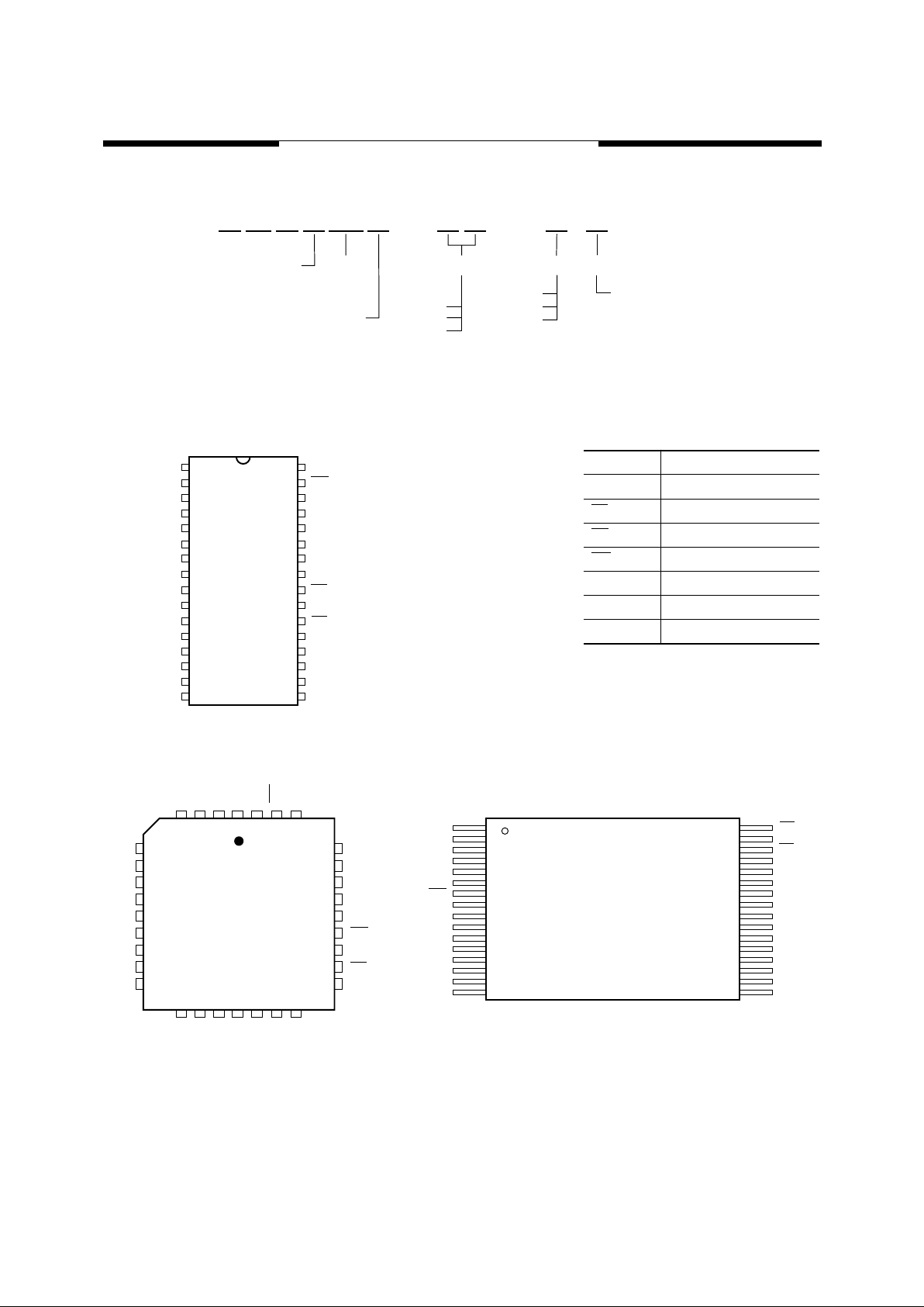
Pin Configurations
N/C
N/C
A15
A12
A7
A6
A5
A4
A3
A2
A1
A0
I/O0
I/O1
I/O2
GND
1
2
3
4
5
6
8
9
10
11
12
13
14
15
16
30
31
32
29
28
27
26
25
7
24
23
22
21
20
32-Pin PDIP
Top View
V
CC
WE
NC
A14
A13
A8
A9
A11
OE
A10
CE
I/O3
I/O4
I/O5
I/O6
I/O7
19
18
17
51001-02
Pin Names
A
0
–A
15
Address Inputs
I/O
0
–I/O
7
Data Input/Output
CE
Chip Enable
OE Output Enable
WE Program Enable
V
CC
5V ± 10% Power Supply
GND Ground
NC No Connect
A
6
A
5
A
4
A
3
A
2
A
1
I/O
0
5
6
7
8
9
10
11
12
13
29
51001-03
28
27
26
25
24
23
22
21
A12A15NCNCVCCWE
NC
A
0
14
I/O
2
GND
I/O
3
I/O4I/O5I/O
6
A
7
A
13
A
8
A
9
A
11
OE
A
10
I/O
7
CE
A
14
I/O
1
32 Pin PLCC
Top View
15 16 17 18 19 20
4 3 2 1 32 31 30
A11
A9
A8
A13
A14
NC
WE
V
CC
N/C
N/C
A15
A12
A7
A6
A5
A4
1
2
3
4
5
6
8
9
10
11
12
13
14
15
16
30
31
32
29
28
27
26
25
7
24
23
22
21
20
32-Pin TSOP I
Standard Pinout
Top View
OE
A10
CE
I/O7
I/O6
I/O5
I/O4
I/O3
GND
I/O2
I/O1
A3
A2
A1
A0
I/O0
19
18
17
51001-04
MOSEL VITELIC
V29C51000T/V29C51000B
3
V29C51000T/V29C51000B Rev. 0.5 October 2000
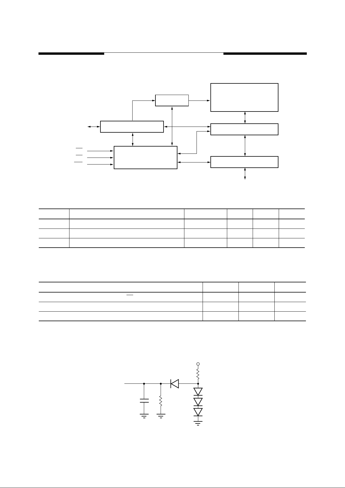
Functional Block Diagram
Capacitance
(1,2)
NOTE:
1. Capacitance is sampled and not 100% tested.
2. T
A
= 25 ° C, V
CC
= 5V ± 10%, f = 1 MHz.
Latch Up Characteristics
(1)
NOTE:
1. Includes all pins except V
CC
. Test conditions: V
CC
= 5V, one pin at a time.
AC Test Load
Symbol Parameter Test mSetup Typ. Max. Units
C
IN
Input Capacitance V
IN
= 0 6 8 pF
C
OUT
Output Capacitance V
OUT
= 0 8 12 pF
C
IN2
Control Pin Capacitance V
IN
= 0 8 10 pF
Parameter Min. Max. Unit
Input Voltage with Respect to GND on A
9
, OE
-1 +13 V
Input Voltage with Respect to GND on I/O, address or control pins -1 V
CC
+ 1 V
V
CC
Current -100 +100 mA
Address buffer & latchesA0–A
15
51001-05
I/O Buffer & Data Latches
I/O
0
–I/O
7
Y-Decoder
65,536 Bit
Memory Cell Array
X-Decoder
Control Logic
CE
OE
WE
51001-06
IN3064 or Equivalent
IN3064
or Equivalent
2.7 kΩ
6.2 kΩ
+5.0 V
IN3064 or Equivalent
IN3064 or Equivalent
CL = 100 pF
Device Under
Test
4
MOSEL VITELIC
V29C51000T/V29C51000B
V29C51000T/V29C51000B Rev. 0.5 October 2000
Absolute Maximum Ratings
(1)
NOTE:
1. Stress greater than those listed unders “Absolute Maximum Ratings” may cause permanent damage to the device. This is a stress
rating only and functional operation of the device at these or any other conditions above those indicated in the operational sections
of this specification is not implied. Exposure to absolute maximum rating conditions for extended periods may affect reliability.
2. No more than one output maybe shorted at a time and not exceeding one second long.
DC Electrical Characteristics
(over the commercial operating range)
Symbol Parameter Commercial Unit
V
IN
Input Voltage (input or I/O pins) -2 to +7 V
V
IN
Input Voltage (A
9
pin, OE
) -2 to +13 V
V
CC
Power Supply Voltage -0.5 to +5.5 V
T
STG
Storage Temerpature (Plastic) -65 to +125
°
C
T
OPR
Operating Temperature 0 to +70
°
C
I
OUT
Short Circuit Current
(2)
200 (Max.) mA
Parameter
Name Parameter Test Conditions Min. Max. Unit
V
IL
Input LOW Voltage V
CC
= V
CC
Min. — 0.8 V
V
IH
Input HIGH Voltage V
CC
= V
CC
Max. 2 — V
I
IL
Input Leakage Current V
IN
= GND to V
CC
, V
CC
= V
CC
Max. —
± 1 µ
A
I
OL
Output Leakage Current V
OUT
= GND to V
CC
, V
CC
= V
CC
Max. —
± 1 µ
A
V
OL
Output LOW Voltage V
CC
= V
CC
Min., I
OL
= 2.1mA — 0.4 V
V
OH
Output HIGH Voltage V
CC
= V
CC
Min, I
OH
= -400 µ A 2.4 — V
I
CC1
Read Current CE
= OE = V
IL
, WE
= V
IH
, all I/Os open,
Address input = V
IL
/V
IH
, at f = 1/t
RC
Min.,
V
CC
= V
CC
Max.
— 40 mA
I
CC2
Program Current CE
= WE = VIL, OE = V
IH
, V
CC
= V
CC
Max. — 50 mA
I
SB
TTL Standby Current CE
= OE = WE = V
IH
, V
CC
= V
CC
Max. — 2mA
I
SB1
CMOS Standby Current CE
= OE = WE = V
CC
– 0.3V, V
CC
= V
CC
Max. — 100
µ
A
V
H
Device ID Voltage for A
9
CE
= OE = VIL, WE = V
IH
11.5 12.5 V
I
H
Device ID Current for A
9
CE = OE = VIL, WE = VIH, A9 = VH Max. — 50 µA
MOSEL VITELIC V29C51000T/V29C51000B
5
V29C51000T/V29C51000B Rev. 0.5 October 2000
AC Electrical Characteristics
(over all temperature ranges)
Read Cycle
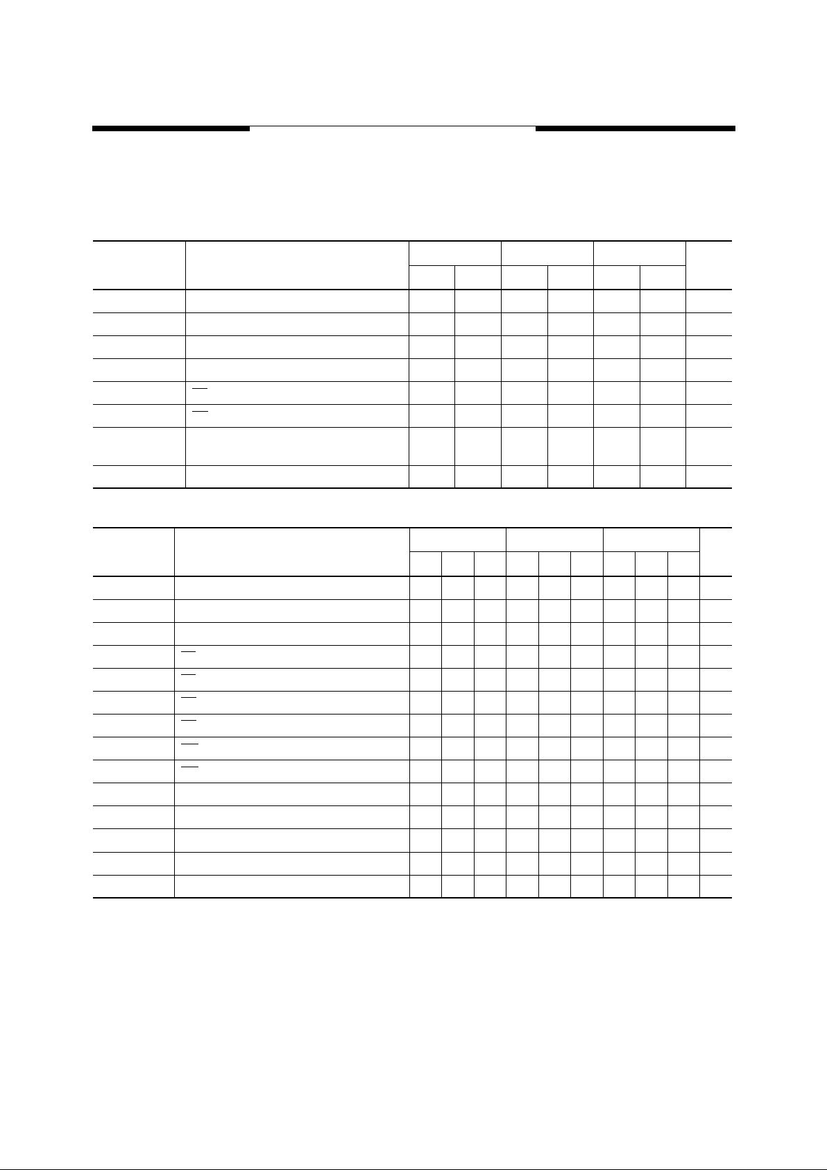
Program (Erase/Program) Cycle
Parameter
Name Parameter
-45 -70 -90
UnitMin. Max. Min. Max. Min. Max.
t
RC
Read Cycle Time 45 — 70 — 90 — ns
t
AA
Address Access Time — 45 — 70 — 90 ns
t
ACS
Chip Enable Access Time — 45 — 70 — 90 ns
t
OE
Output Enable Access Time — 25 — 35 — 45 ns
t
CLZ
CE Low to Output Active 0 — 0 — 0 — ns
t
OLZ
OE Low to Output Active 0 — 0 — 0 — ns
t
DF
Output Enable or Chip Disable to Output in
High Z
020020030ns
t
OH
Output Hold from Address Change 0 — 0 — 0 — ns
Parameter
Name Parameter
-45 -70 -90
UnitMin. Typ. Max. Min. Typ. Max. Min. Typ. Max.
t
WC
Program Cycle Time 45 ——70 ——90 ——ns
t
AS
Address Setup Time 0 —— 0 —— 0 ——ns
t
AH
Address Hold Time 35 ——45 ——45 ——ns
t
CS
CE Setup Time 0 —— 0 —— 0 ——ns
t
CH
CE Hold Time 0 —— 0 —— 0 ——ns
t
OES
OE Setup Time 0 ——0 ——0 ——ns
t
OEH
OE High Hold Time 0 —— 0 —— 0 ——ns
t
WP
WE Pulse Width 25 ——35 ——45 ——ns
t
WPH
WE Pulse Width High 20 ——35 ——38 ——ns
t
DS
Data Setup Time 20 ——25 ——30 ——ns
t
DH
Data Hold Time 0 —— 0 —— 0 ——ns
t
WHWH1
Programming Cycle ——20 ——20 ——20 µs
t
WHWH2
Sector Erase Cycle ——10 ——10 ——10 ms
t
WHWH3
Chip Erase Cycle — 500 ——500 ——500 — ms