

Mosel Vitelic MV20556 Datasheet
MOSEL VITELIC INC.
Preliminary
MV20556
July 1997
Features
General 8051 instruction family compatible
Operate at voltage 5.0V.
No External Memory is supported
8 bit bus I/O ports
4 K byte ROM
128 byte RAM
128 byte depth stack
Two 16 bit Timers (Event Counters)
15 programmable I/O pins
Five interrupt sources
Programmable serial UART channel
Direct LED drive output
Description
The MVI MV20556 is an 8 - bit single chip
microcontroller. It provides hardware features and
powerful instruction set that are necessary to make it a
versatile and cost effective controller for mouse
applications which needs up to 4K byte internal
memory either for program or for data and mixed.
A serial input / output port is provided for I/O
expansion, Inter - processor communications, full
duplex UART.
8 - Bit MCU Mouse Controller
Bit operation instructions
Page free jumps
8 - bit Unsigned Division
8 - bit Unsigned Multiply
BCD arithmatic
Direct Addressing
Indirect Addressing
Nested Interrupt
Two priority level interrupt
A full duplex serial I/O port
Working at 16/25/40 MHz Clock
Full static operation: 3 MHz through 16 MHz
Pin Configuration
1
RES
RXD/P 3.0
TXD/P 3.1
XTA2
XTAL1
#INT0/P 3.2
2
3
4
5
6
MV20556
20L PDIP
300 mil
(Top View)
20
19
18
17
16
15
VDD
P 1.7
P 1.6
P 1.5
P 1.4
P 1.3
#INT1/P 3.3
T0/P 3.4
Ordering Information
MV20556ajk - pqrs
T1/P 3.5
VSS
a: process identifier. { C:=COMS }
jk: working clock in MHz. { 16 }
pqr: production code { 001, ..., 999 }
s: package type. { P: 20L 300 mil PDIP }
Pin/Pad
Postfix
Specifications subject to change without notice, contact your sales representatives for the most recent information.
blank
N
S
Package
dice
20L PDIP
20L SOP
Configuration
page 25
page 1
page 1
Dimension
page 25
page 23
page 24
Logo Size at
Top Marking
-
4.5 x 3.8 mm
4.0 x 3.4 mm
1/27 PID256** 07/97
7
8
9
10
20L SOP
(Top View)
14
13
12
11
P 1.2
P 1.1
P 1.0
P 3.7
MOSEL VITELIC INC.
Block Diagram
Preliminary
MV20556
RES
Vdd
Vss
XTAL2
XTAL1
Timer 1 Timer 0
Reset
Circuit
Power
Circuit
Interrupt
Circuit
Timming
Generator
to pertinent blocks
to whole chip
to pertinent blocks
to whole system
Stack
Pointer
Buffer2
ALU
Decoder &
Register
includes
Acc &
PSW,
Buffer1
128
bits
SFR
etc.
128 bytes
RAM
4K bytes
ROM
Register
Buffer
DPTR
PC
Increamenter
Program
Counter
Port 3
Latch
Port 3
Driver
7
Specifications subject to change without notice, contact your sales representatives for the most recent information.
Port 1
Latch
Port 1
Driver
8
2/27
PID256** 07/97
MOSEL VITELIC INC.
Pin Descriptions
Preliminary
MV20556
20L
PDIP
Pin#
1
2
3
4
5
6
7
8
9
10
11
12
13
14
15
16
17
18
19
20
20L
SOP
Pin#
1
2
3
4
5
6
7
8
9
10
11
12
13
14
15
16
17
18
19
20
dice
Pad#
4
5
6
7
8
9
10
11
12
13-15
17
18
19
20
21
22
23
24
1
2, 3
Symbol
RES
RXD/P3.0
TXD/P3.1
XTAL2
XTAL1
#INT0/P3.2
#INT1/P3.3
T0/P3.4
T1/P3.5
VSS
P3.7
P1.0
P1.1
P1.2
P1.3
P1.4
P1.5
P1.6
P1.7
VDD
Active
L/L/-
I/O
Names
i
Reset
i/o
bit 0 of Port 3 & Receive data
i/o
bit 1 of Port 3 & Transmit data
i
Crystal out
o
Crystal in
i/o
bit 2 of Port 3 & low true Interrupt 0
i/o
bit 3 of Port 3 & low true Interrupt 1
i/o
bit 4 of Port 3 & external input to Timer 0
i/o
bit 5 of Port 3 & external input to Timer 1
i/o
Sink Voltage, Ground
i/o
bit 7 of Port 3
i/o
bit 0 of Port 1
i/o
bit 1 of Port 1
i/o
bit 2 of Port 1
i/o
bit 3 of Port 1
i/o
bit 4 of Port 1
i/o
bit 5 of Port 1
i/o
bit 6 of Port 1
i/o
bit 7 of Port 1
i/o
Drive Voltage, +5 Vcc
Signal Descriptions
Vss
Circuit ground potential.
V
DD
+5V power supply during operation.
PORT 1
Port 1 is an 8-bit quasi-bidirectional I/O port.
There is a pull-up resistance when operating at either
input or output.
PORT 3
Port 3 is an 7-bit quasi-bidirectinal I/O port. It also
contains the interrupt and timer as well as serial port
pins that are used by various options. The output latch
corresponding to a secondary function must be
programmed to one (1) for that function to operate.
The secondary functions are assigned to the pins of port
3, as follows:
- RXD/data (P3.0). Serial port's transmitter data input
(asynchronous) or data input/output (asynchronous).
- TXD/clock (P3.1). Serial port's transmitter data output
(asynchronous) or data input/output (asynchronous).
- #INT0 (P3.2). Interrupt 0 input or gate control input
for counter 0.
- #INT1 (P3.3). Interrupt 1 input or gate control input
for counter 1.
- T0 (P3.4). Input to counter 0.
- T1 (P3.5). Input to counter 1.
There is a pull-up resistance when operating at either
input or output.
RES
A low to high transition on this pin (V IH1) while the
oscillator is not running resets the MV20556. Holding
high signal (higher than V IH1) on this pin for two
machine cycles (24 clocks) or longer while the oscillator
is running, resets the device.
XTAL 1
Input to the oscillator's high gain amplifier. A crystal or
external source can be used.
XTAL 2
Output from the oscillator's amplifier. Required when a
crystal is used.
Specifications subject to change without notice, contact your sales representatives for the most recent information.
3/27
PID256** 07/97

MOSEL VITELIC INC.
Function Overall
Preliminary
MV20556
The CPU of MV20556 manipulates versatile operands in
four memory spaces. They are 4 KB program ROM,
128-byte internal Data RAM, 20 SFRs and 16-bit program
counter.
The Internal Data Memory address space is further
divided into the 128-byte Internal Data RAM and 128-byte
Special Function Register (SFR) address spaces shown in
latter Figures. Four Register Banks (each with eight
registers), 128 addressable bits, and the stack reside in
the Internal Data RAM. The stack depth is limited only by
the available Internal Data RAM and its location is
determined by the 8-bit Stack Pointer. All registers except
the Program Counter and the four 8-Register Banks reside
in the Special Function Register address space.
These memory mapped registers include arithmetic
registers, pointers, I/O ports, and registers for the interrupt
system, timers and serial channel. 128 bit locations in the
SFR address space are addressable as bits. The
MV20556 contains 128 bytes of Internal Data RAM and 20
SFRs.
The MV20556 provides a non-paged Program Memory
address space to accommodate relocatable code.
Conditional branches are performed relative to the
Program Counter. The register-indirect jump permits
branching relative to a 16-bit base register with an offset
provided by an 8-bit index register. Sixteen-bit jumps and
calls permit branching to any location in the contiguous 4K
Program Memory address space.
wide. The MV20556 performs operation on bit, nibble,
byte and double-byte data types.
The MV20556 has extensive facilities for byte transfer,
logic, and integer arithmetic operations. It excells at bit
handling since data transfer, logic and conditional branch
operantions can be performed directly on Boolean
variables.
The MV20556 has five methods for addressing source
operands: Register, Direct, Register-Indirect, Immediate,
and Base-Register-plus Index-Registe -Indirect
Addressing. The first three methods can be used for
addressing destination operands. Most instructions have
a "destination, source" field that specifies the data type,
addressing methods and operands involved. For
operations other than moves, the destination operand is
also a source operand.
Any register in the four 8-Register Banks can be accessed
through Register, Direct, or Register-Indirect Addressing;
the 128 bytes of Internal Data RAM through Direct or
Register-Indirect Addressing; and the Special Function
Registers through Direct Addressing. External Data
Memory is accessed through Register-Indirect
Addressing. Look-Up-Tables resident in Program Memory
can be accessed through Base-Register-plus
Index-Register-Indirect Addressing.
The MV20556 is classified as an 8-bit machine since the
internal ROM, RAM, Special Function Registers,
Arithmetic/Logic Unit and external data bus are each 8 bits
Specifications subject to change without notice, contact your sales representatives for the most recent information.
4/27
PID256** 07/97
MOSEL VITELIC INC.
Preliminary
MV20556
Memory Map Overall
The CPU of MV20556 is able to access three memory areas. They are:
(1) 128 bytes data RAM addressed at 00H through 7FH;
(2) 20 SFRs addressed at 80H through FFH;
(3) 4,096 bytes program ROM addressed at 000H through FFFH.
Be noted, MCU MV20556 builds all accessible memory inside, it is unable to access external memory.
255
128
127
0
Data
RAM
FFH
80H
7FH
00H
255
128
FFH
F0H
Special
Function
Register
Internal Memory Map
Specifications subject to change without notice, contact your sales representatives for the most recent information.
5/27
4095
FFFH
000H0
Internal Program ROMInternal
PID256** 07/97

MOSEL VITELIC INC.
Preliminary
MV20556
Memory Map Details
Internal RAM
The MV20556 contains a 128-byte Internal Data RAM
(Which includes registers R7-R0 in each of four Banks),
and twenty memory-mapped Special Function
Registers.
Internal Data RAM
The Internal Data RAM provides a convenient 128-byte
scratch pad memory.
Register Banks
There are four Register Banks within the Internal Data
RAM. Each Register Bank contains registers R7-R0.
RAM
(MSB) (LSB)
BYTE
7FH
2FH
2EH
2DH
2CH
2BH
2AH
29H
28H
27H
26H
25H
24H
23H
22H
21H
20H
1FH
18H
17H
10H
0FH
08H
07H
00H
7F
77
6F
67
5F
57
4F
47
3F
37
2F
27
1F
17
0F
07
7E
76
6E
66
5E
56
4E
46
3E
36
2E
26
1E
16
0E
06
7D
75
6D
65
5D
55
4D
45
3D
35
2D
25
1D
15
0D
05
7C
74
6C
64
5C
54
4C
44
3C
34
2C
24
1C
14
0C
04
Bank 3
Bank 2
Bank 1
Bank 0
7B
73
6B
63
5B
53
4B
43
3B
33
2B
23
1B
13
0B
03
7A
72
6A
62
5A
52
4A
42
3A
32
2A
22
1A
12
0A
02
79
71
69
61
59
51
49
41
39
31
29
21
19
11
09
01
127
78
47
70
46
68
45
60
44
58
43
50
42
48
41
40
40
38
39
30
38
28
37
20
36
18
35
10
34
08
33
00
32
31
23
24
16
15
8
7
0
128 Addressable Bits
There are 128 addressable software flags in the
Internal Data RAM. They are located in the 16 byte
locations starting at byte address 32 and ending with
byte location 47 of the RAM address space.
Stack
The stack may be located anywhere within the Internal
Data RAM address space. The stack may be as large
as 128 bytes on the MV20556.
7Fh
scratch
pad
area
30h
2Fh
bit
addressable
area
RS1 RS0
11
10
01
00
R7
R0
R7
R0
R7
R0
R7
20h
1Fh
18h
17h
10h
0Fh
08h
07h
Four
bank
area
128B RAM Bit Address 128B RAM Memory Map
Specifications subject to change without notice, contact your sales representatives for the most recent information.
6/27
R0
00h
PID256** 07/97

MOSEL VITELIC INC.
Preliminary
MV20556
Memory Map Details (Cont'd)
Special Function Registers (SFR)
The Special Function Registers include arithmetic
registers (Acc, B, PSW), pointers (SP, DPH, DPL) and
registers that provide an interface between the CPU
and the on-chip peripheral functions. These are also
128 addressable bits within the Special Function
Registers. The memory-mapped locations of these
registers and bits are shown in right side figure.
Acc Register
The Acc register is the accumulator.
B Register
The B register is dedicated during multiply and divide
and serves as both a source and a destination. During
all other operations the B register is simply another
location of the Special Function Register space.
F5
E5
FO
D5
-
B5
-
A5
SM2
9D
95
TF0
8D
85
Bit Addresses
F3
F4
E3
E4
RS0
RS1
D3
D4
PT1
PS
BB
BC
B3
B4
ET1
ES
AB
AC
A3
A4
TB8
REN
9B
9C
93
94
IE1
TR0
8B
8C
83
84
F2
E2
OV
D2
PX1
BA
B2
EX1
AA
A2
RB8
9A
92
IT1
8A
82
F1
E1
D1
PT0
B9
B1
ET0
A9
A1
TI
99
91
IE0
89
81
F0
E0
P
D0
PX0
B8
B0
EX0
A8
A0
RI
98
90
IT0
88
80
Direct
Byte
(MSB) (LSB)
Address
240
224
208
184
176
168
160
152
144
136
128
F7
E7
CY
D7
-
B7
EA
AF
A7
SM0
9F
97
TF1
8F
87
F6
E6
AC
D6
-
B6
-
A6
SM1
9E
96
TR1
8E
86
Hardware
Register
Symbol
B
Acc
PSW
IP
P3
IE
P2
SCON
P1
TCON
P0
Program Status Word Register
The carry (CY), auxiliary carry (AC), user flag 0 (F0),
register bank select (RS0 and RS1), overflow (OV) and
parity (P) flags reside in the Program Status Word
(PSW) Register. These flags are bit-memory-mapped
within the byte-memory-mapped PSW. The PSW flags
record processor status information and control the
operation of the processor.
The CY, AC, and OV flags generally reflect the status
of the latest arithmetic operations. The P flag always
reflects the parity of the Acc register. The carry flag is
also the Boolean accumulator for bit operations.
SYMBOLIC
ADDRESS
Acc
PSW
IPC
P3
IEC
P2
SBUF
SCON
P1
TH1
TH0
TL1
TL0
TMOD
TCON
DPH
DPL
SP
P0
BIT ADDRESS
255
B
247
231
215
191
183
175
167
159
151
143
135
248
240
224
208
184
176
168
160
152
144
136
128
BYTE
ADDRESS
(F0H)
240
(E0H)
224
(D0H)
208
(B8H)
184
(B0H)
176
(A8H)
168
(A0H)
160
(99H)
153
(98H)
152
(90H)
144
(8DH)
141
(8CH)
140
(8BH)
139
(8AH)
138
(89H)
137
(88H)
136
(83H)
131
(82H)
130
(81H)
129
(80H)
128
SFR's
Containing
Direct
Addressable
Bits
SFR Bit Address SFR Memory Map
Specifications subject to change without notice, contact your sales representatives for the most recent information.
7/27 PID256** 07/97
MOSEL VITELIC INC.
Preliminary
MV20556
Memory Map Details (Cont'd)
Program Status Word Register(Cont'd)
F0 is a general purpose flag which is pushed onto the
stack as part of a PSW save. The two Register Bank
select bits (RS1 or RS0) determine which one of the
four Register Banks is selected.
Stack Pointer
The 8-bit Stack Pointer (SP) contains the address at
which the last byte was pushed onto the stack. This is
also the address of the next byte that will be popped.
The SP is incremented during a push. SP can be read
or written to under software control.
Data Pointer (High) and Data Pointer (Low)
The 16-bit Data Pointer (DPTR) register is the
concatenation of registers DPH (data pointer's
high-order byte) and DPL (data pointer's low-order
byte). The DPTR is used in Register-Indirect
Addressing to move Program Memory constants, to
move External Data Memory variables, and to branch
over the 64K Program Memory address space.
Interrupt Enable Register
The Interrupt Enable (IEC) register stores the enable
bits for each of the five interrupt sources. Also included
is a global enable/disable bit of the interrupt system.
Timer/Counter Mode Register
Within the Times Mode (TMOD) register are the bits
that select which operations each timer/counter will do.
Timer/Counter Control Register
The timer/counters are controlled by the Timer/Counter
Control (TCON) register bits. The start/stop bits for the
timer/counters along with the overflow and interrupt
request flags are mapped in TCON.
Timer/Counter 1 (High), Timer/Counter 1 (Low),
Timer/Counter 0 (High), Timer/Counter 0 (Low)
There are four register locations for the two 16-bit
timer/counters. These registers can be read or written
to, to give the programmer easy access to the
timer/counters. TH1 and TH0 refer to the 8 high-order
bits of timer/counter 1 and 0, respectively. TL1 and
TL0 refer to the low-order bits of both timer/counter 1
and 0.
Interrupt Priority Register
The Interrupt Priority (IPC) register contains the control
bits to set an interrupt to a desired level. A bit set to a
one gives the particular interrupt a high priority listing.
Serial Control Register
The Serial Data Buffer (SBUF) register is used to hold
serial port input or output data depending on whether
the serial port is receiving or transmitting data.
PSW definition
MSB
CY AC F0 RS1 RS0 OV - P
CY
AC
F0
RS1
RS0
OV
P
RS1
0
0
1
1
PSW.7
PSW.6
PSW.5
PSW.4
PSW.3
PSW.2
PSW.1
PSW.0
RS0
Carry flag
Auxiliary carry flag
Flag 0 available to the user for general purpose
Register bank selector bit 1.
Register bank selector bit 0.
Overflow flag
Usable as a general purpose flag
Parity flag. Set/clear by hardware at each instruction cycle to indicate an odd/
even number of "1" bus in the accumulator
REGISTER BANK
0
1
0
1
0
1
2
3
ADDRESS
00H-07H
08H-0FH
10H-17H
18H-1FH
LSB
Specifications subject to change without notice, contact your sales representatives for the most recent information.
8/27 PID256** 07/97
MOSEL VITELIC INC.
Preliminary
MV20556
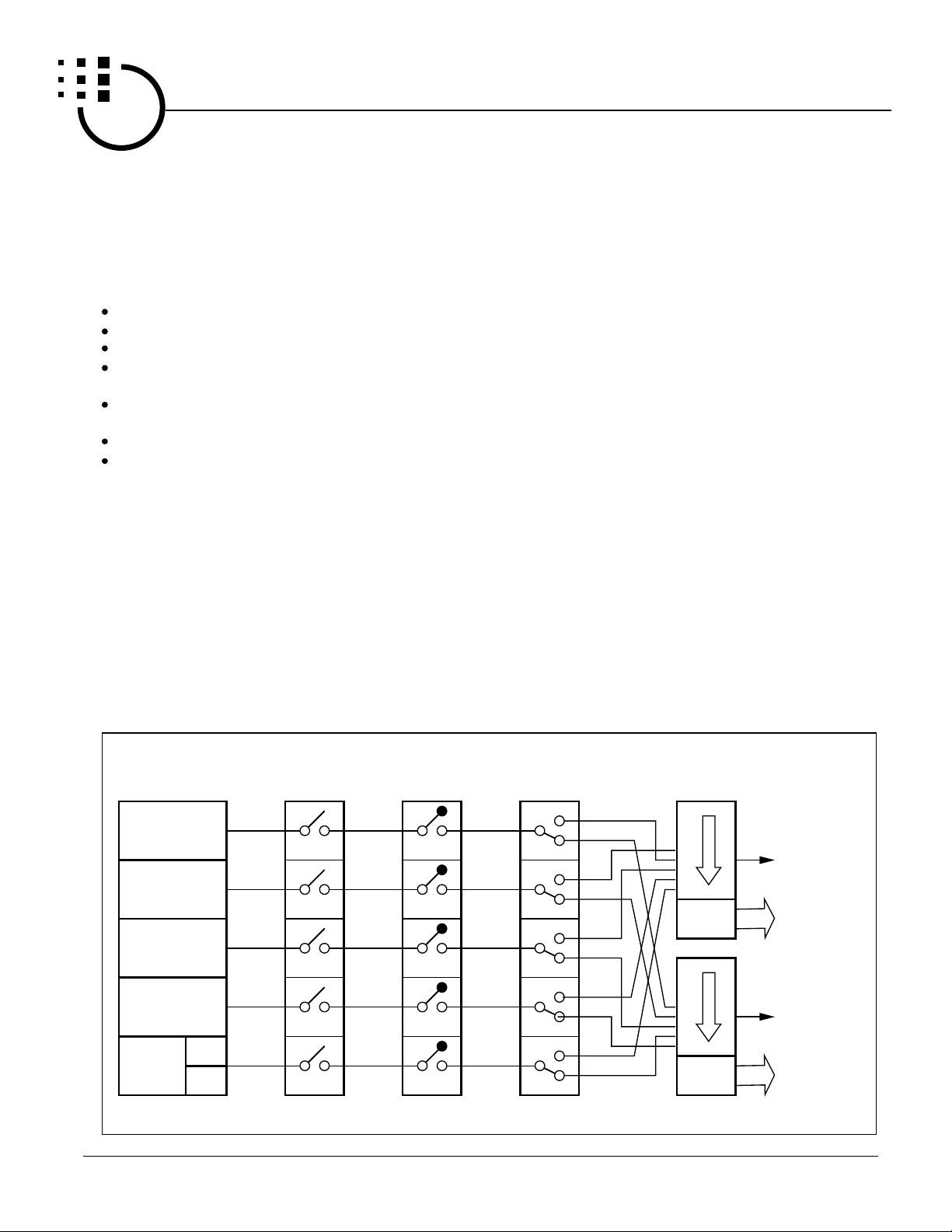
Interrupt System
A sophisticated multiple-source, two-priority-level,
nested interrupt system is provided. The interrupt
system is shown as below diagram. The interrupt
request flag and program memory location of interrupt
service program is shown in table on next page.
Five interrupt sources
Each interrupt can be individually enabled/disabled
Enabled interrupts can be globally enabled/disabled
Each interrupt can be assigned to either of two
priority levels
Each interrupt vectors to a separate location in
program memory
Interrupt nesting to two levels
External interrupt requests can be programmmed to
be level- or transition- activated
Interrupt Overall
External events and the real-time driven onchip
peripherals require service by the CPU asynchronous
to the execution of any particular section of code. To
tie the asynchronous activities of these functions to
normal program execution, a sophisticated
multiple-source, two-priority-level, nested interrupt
system is provided. Interrupt response latency ranges
from 3µs to 7µs when using a 12 MHz crystal.
The MV20556 acknowledges interrupt requests from
five sources: Two from external sources via the #INT0
and INT1 pins, one from each of the two internal
counters and one from the serial I/O port. Each
interrupt vectors to a separate location in Program
Memory for its service program. Each of the five
sources can be assigned to either of two priority levels
and can be independently enabled and disabled.
Additionally all enabled sources can be globally
disabled or enabled. Each external interrupt is
programmable as either level- or transition-activated
and is active-low to allow the "wire or-ing" of several
interrupt sources to the input pin. The interrupt system
is shown diagrammatically in below figure.
Interrupt System Functional Description
Interrupts result in a transfer of control to a new
program location. The program servicing the request
begins at this address. In the MV20556 there are five
hardware sources that can generate an interrupt
request. The starting address of the interrupt service
program for each interrupt source is shown in table on
next page.
A resource requests an interrupt by setting its
associated interrupt request flag in the TCON or SCON
register, as detailed in following table. The interrupt
request will be acknowledged if its interrupt enable bit
in the Interrupt Enable register is set and if it is the
highest priority resource requesting an interrupt. A
resource's interrupt priority level is established as
INPUT LEVEL AND
INTERRUPT REQUEST
FLAG REGISTER:
TCON.1
IE0
TCON.5
TF0
TCON.3
IE1
TCON.7
TF1
SCON.0
TI
SCON.1
RX
Specifications subject to change without notice, contact your sales representatives for the most recent information.
SOURCE
ENABLE
IE.0
EX0
IE.1
ET0
IE.2
EX1
IE.3
ET1
IE.4
ES
GLOBAL
ENABLE
IE.7
EA
INTERRUPT
PRIORITY
REGISTER:
IP.0
PX0
IP.1
PT0
IP.2
PX1
IP.3
PT1
IP.4
PS
9/27 PID256** 07/97
POLLING
HARDWARE
SOURCE
I.D.
SOURCE
I.D.
HIGH PRIORITY
INTERRUPT
REQUEST
VECTOR
LOW PRIORITY
INTERRUPT
REQUEST
VECTOR
 Loading...