

MOSA MS8870 Datasheet
MOSA ELECTRONICS
Features
•
Complete DTMF receiver
•
Low power consumption
• Adjustable guard time
• Central Office Quality
• CMOS, Single 5V operation
O
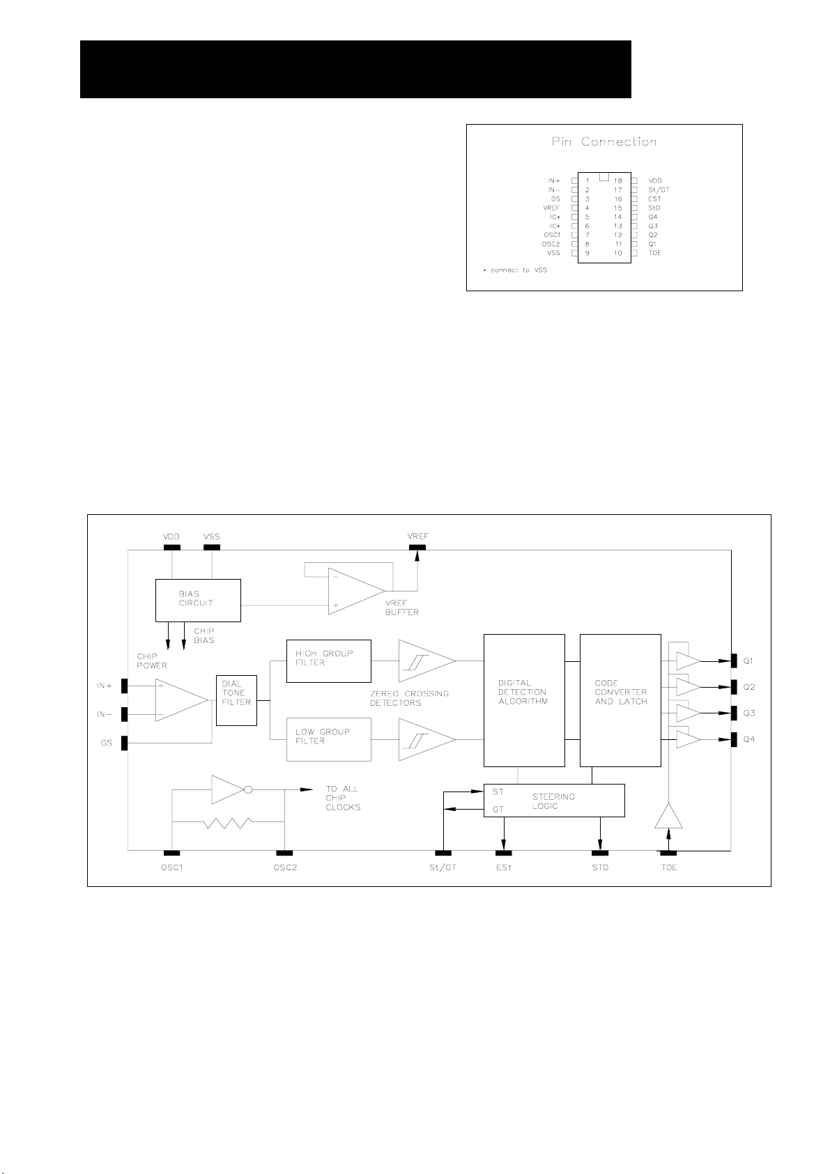
MS8870
DTMF Receiver
rdering Information
MS8870 : 18 PIN DIP PACKAGE
Description
The MS8870 is a complete DTMF receiver integrating
both the bandsplit filter and digital decoder functions,
fabricated in double poly technology and is pin and
function compatible with MITEL8870. The filter section
uses switched capacitor techniques for high and low group
filters; the decoder uses digital counting techniques to
detect and decode all 16 DTMF tone-pairs into a 4-bit code.
External component count is minimized by on chip
provision of a differential input amplifier, clock oscillator
and latched 3-state bus interface.
Figure 1. Functional Block Diagram
- 1 -
MOSA ELECTRONICS
MS8870
DTMF Receiver
Pin Description
Pin # Name Description
1 IN + Non-inverting op-amp input.
2 IN - Inverting op-amp input.
3 GS Gain select. Gives access to output of front end differential amplifier for connection
4 V
5 IC Internal connection. Must be tied to Vss.
6 IC Internal connection. Must be tied to Vss.
7 OSC1 Clock input.
8 OSC2 Clock output. A 3.5795 MHz crystal connected between OSC1 and OSC2 completes
9 Vss Negative power supply input.
10 TOE 3-state output enable (input). Logic high enables the outputs Q1-Q4 Internal pull up.
11-14 Q1-Q4 3-state data output. When enable by TOE, provide the code corresponding to the last
15 StD Delayed steering output. Presents a logic high when a received tone-pair has been
16 ESt Early steering output. Presents a logic high once the digital algorithm has detected a
17 St/GT
18 VDD Positive power supply input.
of feedback resistor.
REF
Reference vo ltage outp ut , nomi nall y VDD /2 is used to bias inputs at mid-rail (see Fig.
2).
the internal oscillator circuit.
valid tone-pair received (see Fig. 5).
registered and the output latch updated; return to logic low when the voltage on St/GT
TS
falls below V
valid tone pair (signal condition). Any momentar y loss of signal condition will cau se
ESt to return to a logic low.
Steering input/guard time output (bi-directional). A voltage greater than V
at St causes the device to register the detected tone pair and update the output latch. A
Voltage less than V
to reset the external steering time-constant; its state is a function of ESt and the
voltage on St.
.
t
TS
frees the device to accept a new tone pair. The GT output acts
t
TS
detected
t
Absolute Maximum Ratings
1 Power supply voltage VDD-Vss 6 V
2 Voltage on any pin Vss - 0.3 VDD + 0.3 V
3 Current at any pin 10 mA
4 Operating temperature -40 +85
5 Storage temperature -65 +150
6 Package power dissipation 1000 mW
Parameter Min Max Units
℃
℃
- 2 -
MS8870
MOSA ELECTRONICS
DTMF Receiver
DC Electrical Characteristics
1 S Operating supply voltage 4.75 5.0 5.25 V
U
2 P Operating supply current IDD 3.0 9.0 mA
P
3 L Power consumption PO 15 45 mW f = 3.58 MHz; VDD= 5V
Y
4 I High level input VIH 3.5 V
5 N Low level input voltage VIL 1.5 V
6 P Input leakage current IIH/IIL 0.1 µA VIN = Vss or VDD
7 U Pull up (source) current ISO 7.5 µA T OE (pin 10) = 0 V
8 T Input impedance (IN+, IN-) RIN 10 MΩ @ 1 KHz
9 S Steering threshold voltage
10 O Low level output voltage VOL 0.03 V No load
11 U Hi gh level output voltage VOH 4.97 V No load
12 T Output low (sink) current IOL 1 2.5 mA V
13 P
14 U
15 T
Output high (
V
V
S
Characteristics Sym Min Typ Max Units Test Conditions
2.2 2.5 V
TS
V
t
OUT
= 0.4V
source
) current
R
output voltage V
ef
R
output resistance
ef
OH
I
0.4 0.8 mA V
2.4 2.8 V No load
R
ef
OR
10 KΩ
R
OUT
= 4.6V
Operating Characteristics
Gain Setting Amplifier
Characteristics Sym Min Typ Max Units Test Conditions
Input leakage current IIN 100 nA Vss ≤ VIN ≤ VDD
Input resistance RIN 10 MΩ
Input offset voltage Vos 25 mV
Power supply rejection PSRR 60 dB 1 KHz
Common mode rejection CMRR 60 dB -3.0V ≤ VIN ≤ 3.0V
DC open loop voltage gain A
Open loop unity gain bandwidth fc 1.5 MHz
Output voltage swing Vo 4.5 Vpp RL ≥ 100KΩ to Vss
Maximum capacitive load (GS) CL 100 pF
Maximum resistive load (GS) RL 50 KΩ
Common mode range VCM 3.0 Vpp No Load
Notes : 1. All voltages referenced to Vss unless otherwise noted.
2. Vcc = 5.0V, Vss = 0V, T
VOL
65 dB
A
= 25 ℃
- 3 -
 Loading...