

Page 1
Application Notes
cable gland
100mm Loop
WiresEnclosure
Radial screen
termination
Cable
Grounded EMI
LVDT Oscillator Demodulator
G123-817-006
1 Scope
These application notes are a guide to applying the
G123-817-006 LVDT Oscillator Demodulator. The following is a
summary of the process that these application notes apply to:
• Select the LVDT you will use.
• Determine the required oscillator level and frequency.
• Wire a test unit for performance checking.
• Optimise performance on the test unit by adjusting oscillator
level, oscillator frequency, phase, output span and output
zero.
• Apply your design.
The G123-817-006 is not a “plug and play” device. It needs to
be carefully optimised for the particular LVDT being used.
LVDT selection criteria and closed loop considerations are not
covered by these application notes.
2 Description
The G123-817-006 is a general purpose LVDT oscillator
demodulator that can be configured to suit a wide variety of
series opposed (4 wire) LVDTs. To produce optimum results,
a knowledge of the characteristics of the LVDT being used is
required.
For a more detailed description refer also to data sheet
G123-817.
The G123-817-006 is an improved version of the
G123-817-002. It does not have a 3.5/8.0V oscillator selector
switch and has improved common mode noise rejection.
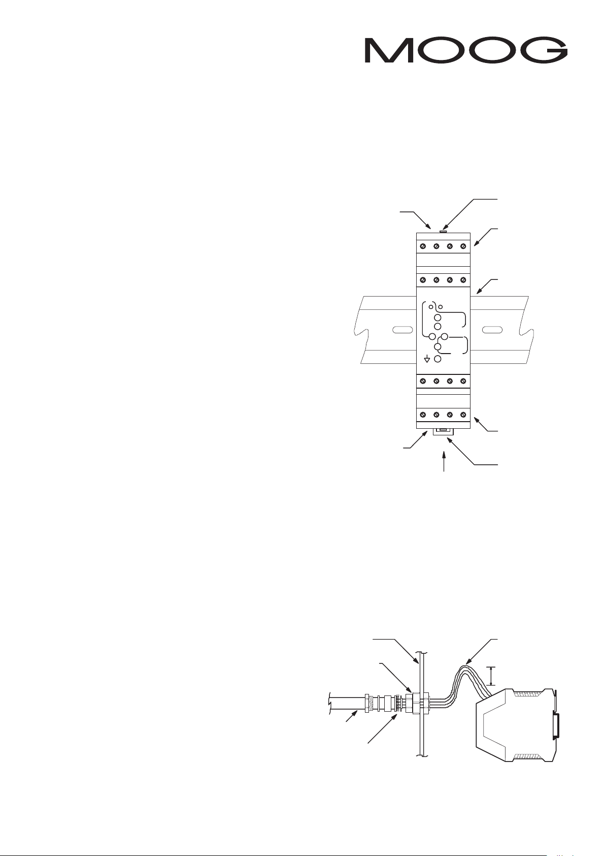
3 Installation
3.1 Placement
A horizontal DIN rail, mounted on the vertical rear surface of
an industrial steel enclosure, is the intended method of
mounting. The rail release clip of the G123-817-006 should
face down, so the front panel and terminal identifications are
readable and so the internal electronics receive a cooling
airflow. An important consideration for the placement of the
module is electro magnetic interference (EMI) from other
equipment in the enclosure. For instance, VF and AC servo
drives can produce high levels of EMI. Always check the
EMC compliance of other equipment before placing the
G123-817-006 close by.
3.2 Cooling
Vents in the top and bottom sides of the G123-817-006 case
provide cooling for the electronics inside. These vents should
be left clear. It is important to ensure that equipment below
does not produce hot exhaust air that heats up the
G123-817-006.
Cover
release
Top vents
Bottom
vents
13 14 15 16
9101112
MOOG
output
Vs
span
zero
Vac
2
level
osc.
LVDT
12 34
56 78
Cooling
airflow
tab (2)
Screw
terminals
9 - 16
DIN rail
Screw
terminals
1 - 8
DIN rail
release
clip
3.3 Wiring
The use of crimp “boot lace ferrules” is recommended for the
screw terminals. Allow sufficient cable length so the circuit
card can be withdrawn from its case with the wires still
connected. This enables switch changes and pot adjustments
on the circuit card to be made while the card is still connected
and operating. An extra 100mm for cables going outside the
enclosure, as well as for wires connecting to adjacent DIN rail
units, is adequate. The LVDT cable should be 3 twisted pairs
with an overall screen.
Preferred wiring
Page 1 of 4: C70880 Rev E – 11.15
Page 2
S2 LEAD/L AG
S1 FREQUENCY
0V
TP2
DMOD
1
1
TP9
TP
3
R6 PHASEADJ.
SEC
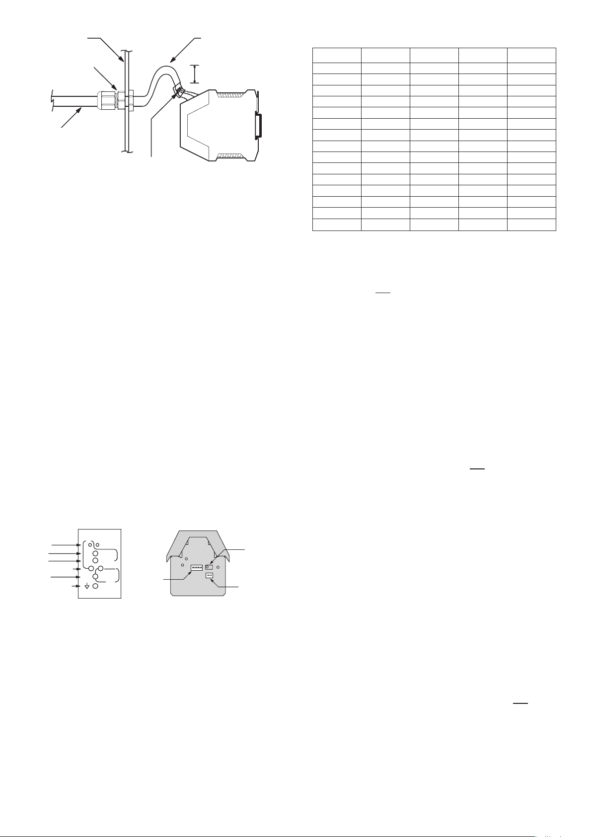
Cable gland
100mm Loop
CableEnclosure
Cable
Wire soldered
to screen
Drain wire.
or
(Heat shrink to
cover the screen)
MOOG
Vac
zero
2
span
LVDT
LEDS
TEST POINTS
POT
POT
POT
output
Vs
level
osc.
TEST POINT
Alternative wiring
3.4 EMC
The G123-817 emits radiation well below the level called for in
its CE mark test. Therefore, no special precautions are required
for suppression of emissions. However, immunity from external
interfering radiation is dependent on careful wiring techniques.
The accepted method is to radially terminate the cable screens,
in an appropriate grounded cable gland, at the point of entry
into the industrial steel enclosure. If this is not possible, chassis
ground screw terminals are provided on the G123-817-006.
Exposed wires should be kept to a minimum length. Connect
the screens at both ends of the cable to chassis ground.
4 Power supply
24V DC nominal, 22 to 28V
60mA @ 24V, without an LVDT connected
160mA @ 22V, with 50mA oscillator load
If an unregulated supply is used, the bottom of the ripple
waveform is not to fall below 22V.
It is recommended that an M205, 250mA T (slow blow) fuse,
compliant with IEC 127-2 sheet 3, be placed in series with the
+24V input on terminal 1 to protect the electronic circuit.
5 Set-up adjustments
Slide S1 and S2 up to turn on.
Front panel potentiometers are 15 turns.
Bold test refers to front panel controls.
Italic test refers to circuit card controls.
Default shipping frequency is 3.1KHz.
Default shipping phase adjustment is zero.
5.1 Excitation frequency
Select the manufacturer’s recommended “zero phase”
excitation frequency with the internal frequency select
switches. The circuit card will need to be withdrawn from
the case to do this. See paragraph six. If the recommended
frequency is not known, start off with 3.1KHz, the default
setting. This is a good starting point because it is an order of
Frequency selection, ✓ = switch on
S1-1 S1-2 S1-3 S1-4 f, kHz
✓ ✓ ✓ 0.8
✓ ✓ ✓ 1.7
✓ ✓ 2.5
✓ ✓ ✓ 3.0
✓ ✓ 3.9
✓ ✓ 4.7
✓ ✓ ✓ 5.1
✓ 5.5
✓ ✓ 5.9
✓ ✓ 6.8
✓ 7.6
✓ ✓ 8.1
✓ 8.9
✓ 9.7
10.5
magnitude greater than the 300Hz electronic bandwidth preset on the circuit card and enables the mechanical bandwidth
to match the electronic bandwidth. Initially, do not select any
phase adjustment. Connect a dual trace oscilloscope to front
panel test point
Vac
and circuit card TP2. Set an oscillator level
2
with the front panel level pot so that the signals are free of
noise and ripple, so a clear, easily read signal is displayed.
Ensure that the level is not so high as to distort the waveform.
Select other frequencies with the frequency select switches to
see if a minimum phase difference can be achieved. Select the
frequency that gives a minimum phase difference. Be aware
that there is an adjustment on the circuit card that reduces the
phase difference so it is not essential to achieve exactly zero
phase difference. Do not turn on all four switches together.
This is an invalid selection.
5.2 Excitation oscillator level
Set the LVDT manufacturer’s recommended excitation oscillator
level with the front panel level pot. The
half of the actual level i.e.2.5V on the test point is equal to a
true 5.0V on the LVDT primary.
The excitation oscillator level is set by the front panel osc.
(oscillator) level potentiometer. Note that the maximum
permissable primary voltage is 8.0V RMS.
Do not set the oscillator level greater than 8.0V RMS. The
maximum permissable LVDT full scale sensitivity is 0.9V/ V. Full
scale sensitivity is defined as the secondary voltage per volt of
primary voltage excitation, when the LVDT core is at full stroke.
With 8.0V RMS osc. voltage the secondary voltage input to the
G123-817-006 must not exceed 7.2V RMS, when the LVDT
core is at full stroke.
There are two limits on the maximum permissable secondary
voltage
• An absolute maximum of 8.0V RMS
• 0.9 times the osc. voltage.
When setting the oscillator level for the first time it is
advisable to observe the oscillator waveform on the
point, with an oscilloscope. For correct operation the waveform
should be a clean sinusoid. Maximum output current is 50mA
RMS. If the waveform is distorted, reduce the level until a clean
sinusoid is observed.
Vac
test point gives
2
Vac
test
2
Page 2 of 4: C70880 Rev E – 11.15
Page 3

LVDT
13
14
9
12
10
1
1
S2-8
2200
pFpF
680
S2-7
1K5
R6100K
10K
S2-1
S2-2
S2-3
S2-4
S2-5
S2-
6
10K
10K
6.8nF
6.8nF
15nF
15nF
47nF
47n
F
TP2
DEMODULATOR
SECONDARY
AMPLIFIER
PHASEADJUSTMENTCIRCUIT
OSCILLATOR
+1
+1 TP3
SECONDARY
SIGNAL
TEST POINT
ADJUST FORMIN IMUM
PHASEDIFFERENC
E
SECONDARY
DEMOD
TEST POIN
T
LEA
D
LA
G
VAC
2
FrontPane
l
2
(P.C.B.)
(P.C.B.
)
Phase adjustment circuit
Example:
Apply the Schaevitz 4000HR LVDT. It has a stroke of ±100mm
and a sensitivity of 8.8mV/ V/mm.
At full stroke of 100mm this equates to a sensitivity of
0.88V/ V.
The manufacturer’s recommended excitation is 3.0V RMS at
2.5kHz.
Adjust the osc. level pot so the output is 3.0V RMS
Vac
(
= 1.5V RMS). The full scale secondary voltage will be
2
3 x 0.88 = 2.64V RMS, just below the secondary maximum of
0.9 x 3.0 = 2.70 VRMS.
If the oscillator level is set to 8.0V RMS, the full stroke
secondary level would be 0.88 x 8 = 7.04V RMS. This is less
than the secondary maximum of 7.2 VRMS and the absolute
maximum of 8.0 VRMS, so the oscillator level can be safely set
up to the maximum of 8.0V RMS.
5.3 Secondary phase difference
The G123-817-006 circuit uses the primary signal to
synchronously detect the secondary signal. Phase differences
between these signals can cause minor errors and so there is
the facility on the circuit card to null phase differences.
Withdraw the circuit card from its case and connect a dual
channel oscilloscope to primary TP
Move the LVDT core until TP2 has a signal that is noise free
and easy to read. The signal will be too small near null.
Determine if the secondary is leading or lagging the primary
signal. Select lead or lag. Do not select lag and lead together.
Now monitor the secondary TP2 and the phase adjusted
secondary demod signal on TP3. Adjust the phase pot R6 until
these two signals are in phase. Select the appropriate lag or
lead capacitors to enable the best phase match. Note that R6
is a 25 turn pot.
Switches S2-7 and S2-8 select the two lag capacitors, which
are switched in parallel. Switches S2-1 to S2-3 and S2-4 to
S2-6 select the lead capacitors, which are switched in series.
To maintain a balanced circuit the switches should be paired in
the same positions. The pairs are 1 and 2, 3 and 4, 5 and 6.
Vac
and secondary TP2.
2
The minimum phase angle varies with frequency and is
typically 3° to 8°. If the phase error is less than 3° to 8°, it
cannot be reduced and so no phase adjustment may give the
minimum phase error.
5.4 Output zero
Move the LVDT core to its required centre position and adjust
the front panel zero pot. until the level on the output test
point is 0V. Set to 12mA if using the 4-20mA signal output.
5.5 Output span
Move the LVDT core to its required full stroke position and
adjust the front panel span pot until the level on the output
test point is 10V. If the polarity is opposite to that required,
interchange the secondary wires on terminals 9 and 12.
Re-check the zero setting. Increasing the oscillator level will
not increase the output. If 10V output cannot be achieved,
consult Moog. Double check the waveform distortion to ensure
the oscillator is not over loaded. Set to 20mA if using the
4-20mA signal output.
6 Withdrawing the circuit card
from its case
In order to set the oscillator frequency, select phase lag or lead,
or to adjust the phase angle, the circuit card needs to be
withdrawn from its case.
To do this, push one tab in with a pen or screwdriver while
gently pulling on the top cover on that side. The cover will
release approximately one mm. Repeat on the other side and
withdraw the cover and circuit card until the required
adjustment points are exposed. The rigidity of the connecting
wires will hold the circuit card in position while adjustments
are made.
Page 3 of 4: C70880 Rev E – 11.15
Page 4

7 Block-wiring diagram
+15V
-15
V
T
P
POWERSUPPLY
1
2
LED
V
S
SPAN
ZER
O
A
B
LED
OUTPU
T
13
14
9
12
10
11
LAG
DEMOD
SECSIGNAL
TP 2
TP 3
SECDEMO
D
PHASE
MEASUREMENT
A
B
RATIOER
DEMO
D
TP
Va
c
AV=0.5
FREQUENC
Y
2
OUTPUT AMP
TP
OUTPU
T
FILTER
OSCILLAT OR
CURRENT
CONVERTER
3
4
7
8
LEAD
PHASE
ADJUS
T
LVDT
+24V DC
SUPPLY
0TO+/-10V
0V
4-20mA
0
V
OUTPUTS
R6
S2-7 &S2-8
SeePhaseAdj.circuit on pg 3.
S1-1 to S1-4
S2-1 to S2-6
0V
5
16
16
250mATfuse
-1
1
22
R
TP
9
6
OSCILLATOR
LEVEL
8 Specifications
Outputs: 0 to ±10V, 1 kOhm min load, terminal 3
4-20mA, 500 Ohm max load, terminal 7
100 PPM/dB excitation rejection
500PPM non-linearity
4mV RMS ripple max @ 3kHz
300Hz bandwidth
Oscillator: 1 to 8.0V RMS
1 to 10kHz
Maximum allowable Terminals 9 and 12
50mA RMS
–50dB THD
200 PPM/ºC frequency TC
secondary voltage: 0.9 x osc. voltage or 8.0V RMS
Front panel Output positive = red
indicators: negative = green
Vs, internal supply = green
Front panel Output ±10V
test points: oscillator Vac , half level
2
Signal 0V
Front panel Output span
trimpots: Output zero
Full scale sensitivity: Min: 0.15 V/ V
Industrial Controls Division. Moog Inc., E
Moog GmbH. Germany. Telephone: 07031-622-0. Fax: 07031-622-100.
Moog Sarl. France. Telephone: 01 45 60 70 00. Fax: 01 45 60 70 01.
Moog Australia Pty. Ltd. Telephone: 03 9561 6044. Fax: 03 9562 0246.
Moog pursues a policy of continuous development and reserves the right to alter designs and specifications without prior notice. Information contained herein is for guidance only and does not form part of a contract.
Australia: Melbourne, Sydney, Brisbane
Ireland: Ringaskiddy
n Italy: Malnate (VA) n Japan: Hiratsuka n Korea: Kwangju-Kun n Philippines: Baguio City n Singapore: Singapore n Sweden: Askim n USA: East Aurora (NY)
Oscillator level
Max: 0.9 V/V
ast Aurora, NY 14052-0018. Telephone: 716/687-4954. Fax: 716/655-1803. Toll Free 1-800-272-MOOG.
n Austria: Vienna n Brazil: S
~
ao Paulo n Denmark: Birkerød n England: Tewkesbury n Finland: Espoo n France: Rungis n Germany: Böblingen, Dusseldorf n Hong Kong: Shatin n India: Bangalore
Internal trimpot: Secondary demodulator
phase adjust R6
Internal switches: Oscillator frequency select S1-1 to -4
Phase lead select S2-1 to -6
Phase lag select S2-7 and -8
Supply: Terminal 1
24V DC nominal, 22 to 28V
60mA @ 24V, no load
160mA @ 22V, with 50mA oscillator load
IP 20
Recommended M205, 250mA T (slow blow) fuse
supply protection: compliant with IEC 127-2 sheet 3
Mounting: DIN rail
Temperature: 0 to +40ºC
Dimensions: 100W x 108H x 22.5D
Weight: 127g
CE mark: EN50081.1 emission
EN61000-6-2 immunity
C tick: AS4251.1 emission
Internet Data
For a detailed Data Sheet and the latest version of this
Application Note please refer to the Moog website
www.moog.com/dinmodules
Page 4 of 4: C70880 Rev E
– 11.15
 Loading...