

MP1010B
L
T
R
R
Cold Cathode Flourescent
Lamp Driver
Monolithic Power Systems
General Description
The MP1010B is a power solution IC that offers a
true complete solution for driving a Cold Cathode
Fluorescent Lamps (CCFL). This Power IC converts
unregulated DC voltage to a nearly pure sine wave
required to ignite and operate the CCFL. Based on
proprietary power topology and control techniques
it greatly increases the power conversion efficiency.
The MP1010B is covered by patent numbers
6,633,138, 6,316,881, and 6,114,814.
Ordering Information
Package Temperature
Part Number∗
MP1010BEM TSSOP20
MP1010BEF TSSOP20F
EV0037
∗ For Tape & Reel use suffix - Z (e.g. MP1010BEM-Z)
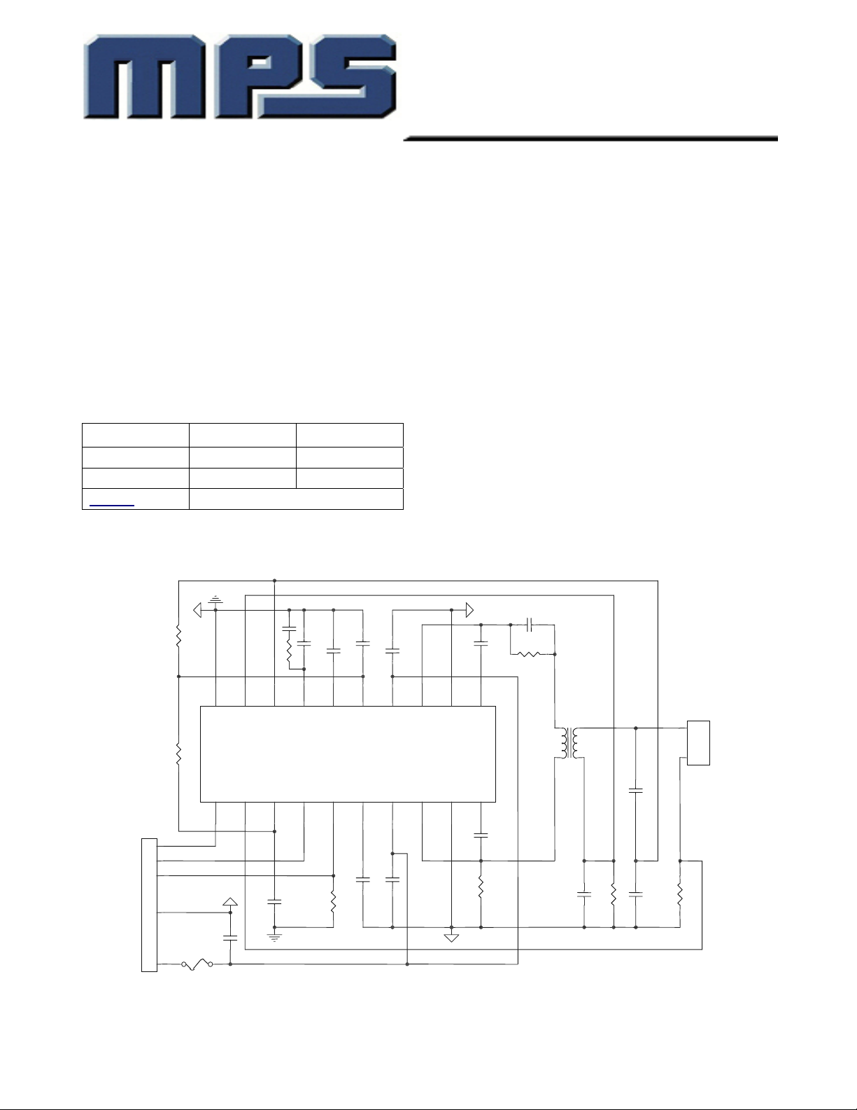
Figure 1: Typical Application Circuit
-20°C to +85°C
-20°C to +85°C
MP1010BEM Evaluation Board
CONFIDENTIAL INFORMATION
Features
Integrated power switches
6.0 to 23V variable supply voltage with
regulated lamp current.
Rated 12W power output at 12V input
Open lamp regulation
Current and Voltage feedback control
Logic Level burst mode control
Supports Open/Short Lamp protection
Soft Start
Output is short circuit protected
High Energy Start Pulse
Analog and Burst Mode Dimming
Evaluation Board Available
Applications
LCD Backlight inverter for notebook computers,
Web Pads, GPS, desktop display, Portable
DVD, Car Video display system.
VBATT
T/B
EN
GND
BR
C8
C2
R2
20 19 18 17 16 15 14 13 12 11
AGND
R1
BR
2
1
J1
5
4
3
2
C15
1
FUSE
R4
C3
C1
F
T/B
MP1010B
R3
FB
O
BOS
IL
3
COMP
EN
R8
C4
REF
DR
C14
C5
C6
IN
OUT
OUTL
IN
865
74
9
C13
C7
BST
PGND
PGND BSTL
10
C12
R7
T1U1
C9
C11
C10
R6
HV
2
1
CN1
R5
MP1010B Rev 1.5 06/25/04 www.monolithicpower.com 1

MP1010B
Cold Cathode Flourescent
Lamp Driver
Monolithic Power Systems
CONFIDENTIAL INFORMATION
Absolute Maximum Ratings
Input Voltage (V
IL, FB Input Voltages (V
OL Input Voltage (V
Logic Input Voltages -0.3V to 6.8V
Power Dissipation 1.0W
Operating Frequency 150KHz
Junction Temperature 150°C
Lead Temperature (Solder) 260°C
Storage Temperature –55°C to 150°C
) 25V
IN
, VFB) +/-6V
IL
) -0.3V to 12V
OL
Recommended Operating Conditions
Input Voltage (V
Analog Brightness Voltage (V
Digital Brightness Voltage (V
Enable (V
EN
Operating Frequency (Typical) 60KHz
Ambient Operating Temperature -20°C to +85°C
Thermal Characteristics
Thermal Resistance (TSSOP) 90° 25° C/W
Thermal Resistance (TSSOPF) 40° 6° C/W
) 6V to 23V
IN
) 0V to 1.9V
BR
) 0V to 1.8V
T/B
) 0V to 5V
θ
JA θJC
Electrical Characteristics (Unless otherwise specified VIN=12V, TA=25°C)
Parameters Symbol Condition Min Typ Max Units
Reference Voltage
Output Voltage V
Reference Current I
Line Regulation
Load Regulation
Output Drivers
Switch On Resistance R
Short Circuit Current ISC 4 A
Ton(min) V
Ton(min) V
Battery Supply
Supply Current (quiescent) I
Supply Current (operating) I
Brightness Control
Sense full Brightness VIL V
Sense full Dim VIL V
Lamp Current regulation 7V < VIN< 23V 2 5 %
Burst Oscillator Peak Voltage V
Digital Brightness Offset Voltage V
Fault Detect
Open Lamp Threshold V
Secondary Current Threshold V
Fault Mode COMP Current I
Shutdown Logic
Fault Timer Threshold V
Fault Timer Sink Current VOL>0, VFB<1.2V 1
Fault Timer Source Current
Open Lamp VOL<0, VFB<1.2V 1
Secondary Overload VFB>1.2V 120 µA
Enable Voltage Low V
Enable Voltage High V
Note 1: This parameter is guaranteed by design.
I
REF
3.0 mA
REF
(ON)
10 µA
CC(OFF)
VIN=23V 1.8 2.5 mA
CC(ON)
1.70 1.78 1.86 V
BOS
-50 5 50 mV
(OS) T/B
0 V
(TH)OL
1.2 V
(TH)FB
V
COMP
1.1 1.2 1.3 V
(TH)FT
= 3mA 4.75 5.0 5.25 V
REF
6.5V < VIN< 23V
0 < I
< 3.0mA
REF
(Note 1)
=0V, VIN=23V 435 550 ns
COMP
=0V, VIN=6V 1750 2100 ns
COMP
= 2.0V 360 379 400 mV
BR
= 0V 105 117 130 mV
BR
<0V, VFB>1.2V 475
OL
0.08 0.11 0.14
30 mV
30 mV
Ω
µA
µA
µA
0.5 V
(L)EN
2.0 V
(H)EN
MP1010B Rev 1.5 06/25/04 www.monolithicpower.com 2

MP1010B
Cold Cathode Flourescent
Lamp Driver
Monolithic Power Systems
CONFIDENTIAL INFORMATION
Pin Description
Table 1: Pin Designators
Pin
Number
1 BR Analog Dimming
2 IL Lamp Current Feedback Sense Input
3 BOS Burst Oscillator Timing
4 T/B Test/Burst Mode Dimming
5 EN Chip Enable. Do not float this pin.
6 DR Internally Generated MOSFET Gate Drive Supply Voltage (6V)
7 IN Power Supply Input
8 OUTL Output to Load (tank circuit)
9 PGND Power Ground
10 BSTL Regulated Output Voltage for Bootstrap Capacitor on Phase L
11 BSTR Regulated Output Voltage for Bootstrap Capacitor on Phase R
12 PGND Power Ground
13 OUTR Output to Load (tank circuit)
14 IN Power Supply Input
15 REF Internally Generated Reference Voltage Output (5V)
16 COMP Loop Compensation Capacitor
17 FT Fault Timer
18 OL Open Lamp Detect (Lamp Voltage Feedback.)
19 FB Shorted Lamp Detect (Secondary Current Feedback)
20 AGND Small Signal Ground (Note 1)
Note 1: For the MP1010BEF, connect the exposed paddle to AGND (Pin 20).
Pin Name Pin Function
BR 1
IL 2
BOS 3
T/B 4
EN 5
DR 6
IN 7
OUTL 8
PGND 9
BSTL 10
20 AGND
19 FB
18 OL
17 FT
16 COMP
15 REF
14 IN
13 OUTR
12 PGND
11 BSTR
MP1010B Rev 1.5 06/25/04 www.monolithicpower.com 3

MP1010B
Cold Cathode Flourescent
Lamp Driver
Monolithic Power Systems
Feature Description
Brightness Control
The MP1010B can operate in three modes:
1. Analog Mode
2. Burst Mode with a DC input
3. Burst Mode with an external PWM.
The three modes are dependent on the pin
connections as per Table 1.
The MP1010B has a soft on and soft off feature to
reduce noise, when using burst mode dimming.
Table 1: Function Mode
Function Pin Connection
Analog Mode 0 – 1.9V V
Burst Mode with
DC input voltage
Burst Mode from
external source
Brightness Polarity:
Burst: 100% duty cycle is at 1.8V
Analog: 1.9V is maximum brightness
Choosing the required burst repetition frequency
can be achieved by an RC combination, as defined
in component selection.
Chip Enable
The chip has an on / off function, which is
controlled by the EN pin (#5). The enable signal
goes directly to a Schmitt trigger. The chip will turn
ON with an EN = High and OFF with an EN = Low.
Pin 1 Pin 4 Pin 3
BR T/B BOS
AGND
REF
0 – 1.8V
V
REF
V
PWM 1.5V
REF
R1
C1
CONFIDENTIAL INFORMATION
Excessive Secondary Current
UL safety specs): The FB pin (#19) is used to
detect whether excessive secondary current has
occurred. During normal operation the FB voltage is
a 1V p-p AC signal centered at zero volts D.C. If a
fault condition occurs that increases the secondary
current, then the voltage at FB will be greater than
1.2V. When that occurs, the IC regulates the FB
voltage to 2.4V p-p and a 120µA current source will
inject into the FT pin. If the voltage at the FT pin
exceeds 1.2V, the chip will shut down.
Lamp Startup
The strike voltage of the lamp will always be
guaranteed at any temperature because the
MP1010B uses a resonant topology for switching
the outputs. The device will continue to switch at
the resonant frequency of the tank until the strike
voltage is achieved. This eliminates the need for
external ramp timing circuits to ensure startup.
Fault Timer
The timing for the fault timer will depend on the
sourcing current, as described above, and the
capacitor on the FT pin. The user can program the
time for the voltage to rise before the chip detects a
“real“ fault. When a fault is triggered, then the
internal drive voltage (V
to 0V. The reference voltage will stay high at 5.0V.
(Shorted Lamp and
) will collapse from 6.2V
DR
Fault Protection
Open Lamp: The OL pin (#18) is used to detect
whether an open lamp condition has occurred.
During normal operation the OL pin is typically at
5V DC with an AC swing of +/- 2V. If an open lamp
condition exists then the AC voltage on the OL line
will swing below zero volts. When that occurs, the
IC regulates the OL voltage to 10V p-p and a 1µA
current source will inject into the FT pin. If the
voltage at the FT pin exceeds 1.2V, the chip will
shut down.
MP1010B Rev 1.5 06/25/04 www.monolithicpower.com 4

MP1010B
Cold Cathode Flourescent
Lamp Driver
Monolithic Power Systems
Packaging Information
TSSOP20 or TSSOP20F (Exposed Paddle **)
0.0256(0.650)TYP
PIN 1
IDENT.
0.030(0.750)
0.150(3.80)
0.165(4.19)
0.105 (2.67)
0.118 (3.00)
0.169
0.177
(4.300)
(4.500)
0.244
0.260
(6.200)
(6.600)
CONFIDENTIAL INFORMATION
0.004(0.090)
0.010(0.250)
GATE PLANE
0.004(0.090)
o
0o-8
0.018(0.450)
0.030(0.750)
0.039(1.000)REF
DETAIL "A"
0.030(0.750)
SEE DETAIL "B"
** EXPOSED PADDLE VERSION ONLY
SEE DETAIL "A"
0.252 (6.400)
0.260 (6.600)
0.033(0.850)
0.047(1.200)
0.007(0.190)
0.012(0.300)
NOTE:
1) Control dimension is in inches. Dimension in bracket is millimeters.
0.032(0.800)
0.041(1.050)
0.002(0.050)
0.006(0.150)
SEATING PLANE
0.004(0.090)
0.006(0.160)
0.075(0.190)
0.012(0.300)
0.004(0.090)
0.008(0.200)
0.007(0.190)
0.010(0.250)
DETAIL "B"
NOTICE: MPS believes the information in this document to be accurate and reliable. However, it is subject to change
without notice. Please contact the factory for current specifications. No responsibility is assumed by MPS for its use or fit
to any application, nor for infringement of patent or other rights of third parties.
MP1010B_Rev 1.5 Monolithic Power Systems, Inc. 5
06/25/04 983 University Ave, Building A, Los Gatos, CA 95032 USA
© 2004 MPS, Inc. Tel: 408-357-6600
♦
Fax: 408-357-6601 ♦ www.monolithicpower.com
 Loading...