


Agile RF Synthesizer & AOM driver
ARF021/ARF421, XRF021/XRF421
Version 1.3.0, Rev 2, 3 and 4.

Limitation of Liability
MOG Laboratories PtyLtd (MOGLabs) does notassume any liability arising out of the use of the information contained within this
manual. This document may contain or reference information and
products protected by copyrights or patents and does not convey
any license under the patent rights of MOGLabs, nor the rights of
others. MOGLabs will not be liable for any defect in hardware or
software orlossor inadequacyofdata ofanykind, orfor anydirect,
indirect, incidental, or consequential damages in connections with
or arising out of the performance or use of any of its products. The
foregoing limitation of liability shall be equally applicable to any
service provided by MOGLabs.
Copyright
Copyrightc MOG Laboratories Pty Ltd (MOGLabs) 2015–2017.
No part of this publicationmay be reproduced, stored ina retrieval
system, or transmitted, in any form or by any means, electronic,
mechanical, photocopying or otherwise, without the prior written
permission of MOGLabs.
Contact
For further information, please contact:
MOG Laboratories P/L
Suites 34–35
49 University St
Carlton VIC 3053
AUSTRALIA
+61 3 9939 0677
info@moglabs.com
www.moglabs.com
MOGLabs USA LLC
419 14th St
Huntingdon PA 16652
USA
+1 814 251 4363
info@moglabsusa.com
www.moglabsusa.com
MOGLabs Europe
Goethepark 9
10627 Berlin
Germany
+49 30 21 960 959
info@@moglabs.eu

Preface
Acousto-opticmodulators (AOMs)areanintegralpartofmanylaserbased experiments. They are used for frequency shifting, amplitude
modulation,andlaserfrequencystabilisation. Many experimentsrequire very simple control of the RF frequency and power, but others
require sophisticated sequences. The MOGLabs ARF/XRF agile RF
synthesizer provides such complexity with a user-friendly interface.
The extraordinary capabilities of the ARF/XRF have not previously
been available from any single supplier, let alone in a single unit.
Two channels, with direct output of up to 4W per channel. Wide
frequency range of 20 to 400MHz. Arbitrary frequency, amplitude
and phasewith highresolution. Analogue modulation ofeach channel, in frequency,amplitude, and/or phase,with 10MHz bandwidth.
Ergonomic front-panel controls, and ethernet/USB interface. Tablemode operation to define complextime-dependent waveform output.
All in one box which connects directly to AC mains power and to
yourAOMs. Asyoudelveintothismanualyouwilluncovermore and
more capability, but the powerful FPGA at the heart of the ARF/XRF
allows software improvements to add new features, so please check
the MOGLabs website for updates, example code, and assistance.
We hope that you enjoy using the ARF/XRF, and please let us know
if you have any suggestions for improvement in the ARF/XRF or in
this document, so that we can make life in the lab better for all.
MOGLabs, Melbourne, Australia
www.moglabs.com
i

ii

Safety Precautions
Safe andeffectiveuseof thisproductisvery important. Please read
the following safety information before attempting to operate. Also
please note several specific and unusual cautionary notes before
using the MOGLabs ARF/XRF, in addition to the safety precautions
that are standard for any electronic equipment.
CAUTION Toensure correctcoolingairflow,the unitshould notbe oper-
ated with cover removed.
WARNING High voltages are exposed internally, particularly around the
mains power inlet and internal power supply unit. The unit
should not be operated with cover removed.
NOTE The MOGLabs ARF/XRF is designed for use in scientific re-
search laboratories. It should not be used for consumer or
medical applications.
iii

Protection Features
The MOGLabsARF/XRF includes anumber offeaturesto protectyou
and your device.
Open/short circuit Each RF output should be connected to a 50Ω load. The AR-
F/XRF will disableeachhigh-powerRF output ifnot connected
or if a short-circuit is detected.
Reflected power The RF reflected power and VSWR (voltage standing wave
ratio)are monitoredandRFoutputisdisabledifeitherexceeds
their safe limit settings.
Mains filter Protection against mains transients.
Temperature Several temperaturesensors controlthe fanand willtrigger a
shutdown if the temperature exceeds a safe limit.
iv

Contents
Preface i
Safety Precautions iii
Protection Features iv
1 Introduction 1
1.1 Operating modes . . . . . . . . . . . . . . . . . . . . . 2
1.2 RF on/off control . . . . . . . . . . . . . . . . . . . . . 4
2 Connections and controls 5
2.1 Front panel controls . . . . . . . . . . . . . . . . . . . 5
2.2 Front panel display/monitor . . . . . . . . . . . . . . . 6
2.3 Rear panel controls and connections. . . . . . . . . . 7
2.4 Internal DIP switches . . . . . . . . . . . . . . . . . . 8
3 Communications 11
3.1 Protocol . . . . . . . . . . . . . . . . . . . . . . . . . . 11
3.2 TCP/IP . . . . . . . . . . . . . . . . . . . . . . . . . . . 13
3.3 USB . . . . . . . . . . . . . . . . . . . . . . . . . . . . 14
4 MOGRF host software 17
4.1 Device discovery . . . . . . . . . . . . . . . . . . . . . 17
4.2 Device commander . . . . . . . . . . . . . . . . . . . . 18
4.3 MOGRF main window . . . . . . . . . . . . . . . . . . 19
4.4 Table viewer . . . . . . . . . . . . . . . . . . . . . . . . 23
4.5 External I/O settings . . . . . . . . . . . . . . . . . . . 24
5 External modulation 27
5.1 Operational principle. . . . . . . . . . . . . . . . . . . 27
5.2 Modulation gain . . . . . . . . . . . . . . . . . . . . . 28
v

vi Contents
5.3 Dual modulation: fast and slow modes . . . . . . . . 29
5.4 Examples. . . . . . . . . . . . . . . . . . . . . . . . . . 30
6 PID stabilisation 35
6.1 Signal conditioning . . . . . . . . . . . . . . . . . . . . 35
6.2 PID control loop . . . . . . . . . . . . . . . . . . . . . 36
6.3 Dual modulation with PID . . . . . . . . . . . . . . . 37
6.4 Noise-eater implementation . . . . . . . . . . . . . . . 38
6.5 Example . . . . . . . . . . . . . . . . . . . . . . . . . . 39
7 Digital I/O 41
7.1 DB15 connector . . . . . . . . . . . . . . . . . . . . . . 41
7.2 High-speed digital . . . . . . . . . . . . . . . . . . . . 43
7.3 Configuration . . . . . . . . . . . . . . . . . . . . . . . 44
7.4 TTL switching . . . . . . . . . . . . . . . . . . . . . . . 46
7.5 External switching timing . . . . . . . . . . . . . . . . 48
7.6 Counters . . . . . . . . . . . . . . . . . . . . . . . . . . 50
7.7 Examples. . . . . . . . . . . . . . . . . . . . . . . . . . 51
8 Simple table mode 53
8.1 Operational principle. . . . . . . . . . . . . . . . . . . 53
8.2 Defining table entries . . . . . . . . . . . . . . . . . . 54
8.3 Digital I/O . . . . . . . . . . . . . . . . . . . . . . . . . 57
8.4 Loops and triggers . . . . . . . . . . . . . . . . . . . . 62
8.5 Upload and download . . . . . . . . . . . . . . . . . . 65
8.6 Re-arm and restart . . . . . . . . . . . . . . . . . . . . 66
8.7 Linear ramps . . . . . . . . . . . . . . . . . . . . . . . 67
8.8 Synchronous table execution . . . . . . . . . . . . . . 69
9 Advanced table mode (XRF) 71
9.1 Operational principle. . . . . . . . . . . . . . . . . . . 71
9.2 Defining table entries . . . . . . . . . . . . . . . . . . 72
9.3 Initial and final states . . . . . . . . . . . . . . . . . . 76
9.4 Counters . . . . . . . . . . . . . . . . . . . . . . . . . . 77
9.5 Loops and triggers . . . . . . . . . . . . . . . . . . . . 78
9.6 Linear ramps using extrapolation . . . . . . . . . . . . 79
9.7 Frequency gain . . . . . . . . . . . . . . . . . . . . . . 81
9.8 Other instruction parameters . . . . . . . . . . . . . . 83

Contents vii
9.9 Additional examples . . . . . . . . . . . . . . . . . . . 84
A Specifications 89
B Firmware upgrades 91
B.1 Firmware components . . . . . . . . . . . . . . . . . . 91
B.2 Factory reset . . . . . . . . . . . . . . . . . . . . . . . 92
B.3 Upgrade via mogrffw . . . . . . . . . . . . . . . . . . 92
B.4 Upgrade via web interface . . . . . . . . . . . . . . . . 94
B.5 Upgrading an ARF to an XRF . . . . . . . . . . . . . . 96
C Command language 97
C.1 Arguments . . . . . . . . . . . . . . . . . . . . . . . . . 97
C.2 General functions . . . . . . . . . . . . . . . . . . . . . 98
C.3 Basic control . . . . . . . . . . . . . . . . . . . . . . . 98
C.4 Primary RF control . . . . . . . . . . . . . . . . . . . . 99
C.5 Modulation . . . . . . . . . . . . . . . . . . . . . . . . 101
C.6 Digital ramp generator. . . . . . . . . . . . . . . . . . 102
C.7 Monitor outputs . . . . . . . . . . . . . . . . . . . . . . 104
C.8 Clock reference . . . . . . . . . . . . . . . . . . . . . . 104
C.9 Table mode . . . . . . . . . . . . . . . . . . . . . . . . 106
C.10 PID feedback . . . . . . . . . . . . . . . . . . . . . . . 108
C.11 External IO functions . . . . . . . . . . . . . . . . . . . 110
C.12 Configuration settings . . . . . . . . . . . . . . . . . . 112
C.13 Direct DDS control . . . . . . . . . . . . . . . . . . . . 112
D Code examples 115
D.1 python . . . . . . . . . . . . . . . . . . . . . . . . . . . 115
D.2 matlab . . . . . . . . . . . . . . . . . . . . . . . . . . . 117
D.3 LabVIEW . . . . . . . . . . . . . . . . . . . . . . . . . . 118

viii Contents

1. Introduction
The MOGLabs ARF/XRF consists of two independent AD9910 direct
digital synthesizer (DDS) sources, each with 4W amplifier. The
frequency,amplitudeandphaseofeachoutputissoftware-controlled
viaa microcontrollerandFPGA(fieldprogrammablegatearray). This
enables direct control of the frequency, amplitude and phase of the
RF signals, which canbeadjusted inreal-time usingthefront-panel
control knobs, orvia ascripting languageover ethernetor USB.The
RF parameters canbedefined inalookup table(loadedvia ethernet
or USB) to enable complex sequences with very fast transitions.
The block diagram below shows the key components. The RF signal output from each DDS is low-pass filtered, pre-amplified, and
FPGA
Front Panel Display & Control
Local
Oscillator
Micro
controller
DDS + RF
AD9910 DDS
LP lter
RF switch
RF amplier
Power detector
DAC
Output
A/D
(2 per channel)
RF on/o
7-pole lters
10MHz
External
Clock
Ethernet
10/100
Fast RAM
table memory
USB
RF OUT
4x MOD IN
RF on/o
RAM table
memory
1

2 Chapter 1. Introduction
then further amplified with a GaN hybrid high-power output stage
(ARF421/XRF421 only). The RF signals are monitored to checkoutput
power and to measure the reflection (VSWR).
TheDDS chipsarecontrolledbytheFPGA.Amicrocontrollerprovides
external interfacewith TCPIP and USB communications, and controls
the front-panel display, rotary encoders (knobs) and push-buttons.
The device allows analogue modulation through two analogue-todigital converters (ADC) with anti-aliasing filters. When modulation
is enabled, the FPGA periodically reads the value of the modulation
signal and uses that value to reprogram the DDS frequency, power
and/or phase.
The ARF/XRF includes memory for storing complex waveform sequences, where each step in the sequence can include frequency,
power, phase, time delay, and more complex definitions of ramps
and other time-dependent functions. Complex capabilities can be
accessed via either TCPIP or USB communications. See Chapter 3
for information on communications options and setup.
Oncecommunicationsareestablished,theARF/XRF canbe controlled
with simple text commands. The commands can be very basic, for
exampleto definethefrequencyorpower,orthey candefinecomplex
dynamicsequences. AppendixCprovidesasummaryoftheavailable
commands.
1.1 Operating modes
The ARF/XRF can be used at varying levels of complexity, as either
a free-running RF source or to follow pre-determined instructions
defined in a table. The modes of operation are outlined below, and
thecurrentoperationalmode ofeach channelcanbe individuallyset
using the MODE command.

1.1 Operating modes 3
NSB: Basic mode
Default state on power-up. In this mode, each channel acts as a
simple single-frequency RF source, with the DDS chips controlled
directly by the FPGA. The frequency and power of the signal can
be controlled via the front panel, using simple instructions over the
computer interface (e.g. FREQ or POW), or using the modulation inputs. Basic mode is convenient for driving AOMs and other singlefrequency devices,with theflexibilityofmodulation andPID control.
NSA: Advanced mode
Advanced modeprovidesdirect user-control of eachDDS through its
internal registersviathe DDS command. Directprogramming ofeach
DDS is complexand not necessary for most applications; it requires
careful reference tothe AD9910 datasheet and manualcalculation of
the hardware registers.
TSB: Simple table mode
In table mode, the RF parameters are automatically sequenced by
the FPGA according to a table of values pre-loaded by the microcontroller and steppedthrough automatically. The table entries are
defined by simple text commands from the host computer which define the RF frequency, amplitude, phase and any I/O behaviour, as
detailed in chapter 8. The minimum duration of a TSB entry is 1µs
and each table can comprise up to 8191 instructions.
TPA: Advanced table mode
XRF models provide a more advanced table mode with greatly im-
proved timing resolution and single parameter updates at 16ns intervals. Smooth pulses can be generated with precise control of
the envelopethrough piecewise-linearinterpolation. Details onadvanced table mode functionality are described in chapter 9.

4 Chapter 1. Introduction
1.2 RF on/off control
The RF output can be turned on and off via software control of the
DDS generators (through the POW command), but for many applica-
tions that is too slow, and the extinction ratio is inadequate. The
ARF/XRF has additional hardware-basedon/offcontrol ontheoutput
of each DDS, using an RF switch before the amplifiers.
Thishardwareswitchshort-circuitstheRFoutputoftheDDS,andcan
becontrolledviaacombinationof softwareandhardwareinputs (see
§7.5). In this way, the RF can be controlled using the front panel,
the ON/OFF commands, as well as via table entries with appropriate
flags.
There is additional control of the DC supplies to the high-power RF
amplifiers to furtherimprove the extinction ratio. The response time
is significantlylongerthan justswitchingthe RF signal, butreduces
the RF noise on the output.

2. Connections and controls
2.1 Front panel controls
CHANNEL 1
FREQUENCY POWERFREQUENCY POWER
STATUS
STATUS
CHAN 1
CHAN 2
STATUS
CHANNEL 2
OFF
ON
OFF
ON
Agile RF Synthesizer
POWER
Frequency The frequency encodercan beused toadjustthe frequencyfor each
RF channel, when operating in NSA mode. The current frequency is
displayed on the LCD display.
Power Similarly, the output power can be adjusted for each channel.
OFF/ON The RF output can be enabled or suppressed with the push-button
off/on switch for each channel.
STATUS Each channel has a multi-colour status LED indicator whose colour
indicates the current output state of the channel as follows.
Colour DDS signal Amplifiers
Off Off Off
Green On On
Yellow On Off
Blue Off On
Red Error state
5

6 Chapter 2. Connections and controls
2.2 Front panel display/monitor
The LCD display shows key information including frequency and
power for each channel, and ethernet information.
STATUS Indicator displaying the status of the microcontroller.
• Blinking green: Normal operation, no faults
• Green/blue: Normal operation, device is initialising
• Blue: Microcontroller unresponsive, unknown state
• Red/orange: Critical fault, diagnosis available
• Red: Critical fault, comms unavailable
In the event of an unresponsive unit, for example following a failed
firmware update, please contact MOGLabs for assistance.
CHAN 1, CHAN 2 Indicator displaying the current mode of the channel.
• Off: Channel disabled/FPGA inactive
• Red: Criticalerror,channeldisabled(e.g. outputdisconnected)
• Green: NSB mode, normal operation (front-panel enabled)
• Light blue: NSA mode, direct control of DDS (no front-panel)
• Blue: TSB mode, simple table mode (limited front-panel)
• Blinking: Non-critical error (e.g. PID saturation limit)
POWER Indicator displaying the status of the power supply
• Off: No power to unit
• Green: Unit is starting up
• Light blue: Normal operation
• Orange: Supply voltages outside expected range
• Red: Critical error with supply
Push-buttons There are four push-buttons on the righthand side of the LCD dis-
play, which are presently of limited functionality. Pressing the ↑/↓
keyscyclesthroughtheoperationalmodesof CH1/CH2respectively.

2.3 Rear panel controls and connections 7
2.3 Rear panel controls and connections
RF OUT
FREQ 1 FREQ 2 CLK INRF OUT 1 RF OUT 2
AMP 1 AMP 2 MOD OUTMON 1 MON 2
MOD IN
SN:
90–264Vac 47–63Hz
WARNING: TheSMA connectors on the back-panel are surface-mounted tothe PCB
inside the unit. Do not apply excessive force during tightening as this will break
the connector off the PCB. Finger-tightening is sufficient for the frequency range of
the ARF/XRF and use of a wrench or spanner is strongly discouraged. The maximum
recommended torque is 0.6Nm.
IEC power in/out The ARF is compatible with all standard AC power systems, from 90
to 264V and 47 to 63Hz. The maximum current is about 1A.
Fan TheARFhasthreetemperature-controlledfansdirectingairflowover
the RF power amplifiers and the FPGA, exhausting through the rear
vent. Ensure that the vent does not become blocked.
RF OUT Thereare twoprimary RF outputsand twosecondary RF outputs for
monitoring. The high-power outputs are labelled RF OUT 1 and RF
OUT 2, and should be 50Ω terminated.
MON Separately buffered RF outputs for monitoring, at −20dBc to each
main output when high-impedance terminated.
MOD IN Each RF channel has two associated analogue inputs, FREQ and
AMP, nominally for frequency and amplitude modulation. The AMP
inputcanbe reconfiguredto performphase modulationusing theMDN
command. Thesemodulationinputscanbeusedforlasernoise-eater
or frequency stabilisation applications (see chapter 5).

8 Chapter 2. Connections and controls
CLK IN The ARF uses a high stability OCX crystal clock, but can also be
synchronisedtoahigh-performance externalclock (5MHzto1GHz)
input via this connector. The input is 50Ω terminated. The signal
should be 1V p-p, and preferably square-wave.
MOD OUT The ARF/XRF provides three analogue outputs, ±2.5V, with 14-bit
resolution and 1MHz bandwidth, for monitoring purposes. One is
available at the MOD OUT SMA connector; the other two can be
accessed from the DB15 connector.
DB15 The DB15 connector provides basic I/O functionality. There are TTL
inputsforquicklysuppressingtheRF output,andTTLoutputsforcontrollingexperimentaldevicessuchas shutters. Twogeneral-purpose
analogueoutputs, similarto MODOUT,arealsoavailable. The connector pinout is described in §7.1. The B3110 breakout board is
available to provide convenient SMA connectors for the different I/O
channels.
RJ45/USB-A Ethernet (TCP/IP 10/100Mb/s) and USB communications jacks.
2.4 Internal DIP switches
Four DIP switches are provided to assist in diagnosis and recovery
of the ARF/XRF units.
WARNING There is potential for exposure to high voltages inside the ARF/XRF.
Take care around the power supply and ensure that objects, particularly electrically conducting objects, do not enter the unit.
CAUTION The cover should be left on to ensure proper airflow and cooling.
OFF ON
1 Normal operation Legacy firmware update mode
2 Disable FPGA Normal operation
3 Use factory settings Normal operation
4 Normal operation Factory reset

2.4 Internal DIP switches 9
DIP 1 Default OFF. If switched ON, the unit will start in legacy firmware
uploadmode. Connecttothedeviceusingaweb-browserandupload
firmware to the microcontroller. It is strongly recommended to use
mogrffw to update the firmware as described in Appendix B; this
option is only provided as a fallback option in case mogrffw fails.
DIP 2 DefaultON.NormaloperationrequiresthatanFPGA imagebeloaded
fromFLASH memoryintotheFPGA,whichtakes10–20s. Intheevent
ofacorruptFPGA image, disableDIP 2 andapplyafirmwareupdate.
DIP 3 Default ON. Device settings, including network settings, are stored
in EEPROM and loaded on startup. If invalid settings are saved to
EEPROM, disable DIP 3 to load factory defaults to facilitate debug-
ging and diagnostics.
DIP 4 Default OFF. Switch ON and reboot to restore the unit to factory
settings. Firmware for both microcontroller and FPGA, as well as
the EEPROM settings, will be restored.

10 Chapter 2. Connections and controls

3. Communications
TheARF canbeconnected toa computerbyUSB orethernet (TCPIP).
The software package mogrf (chapter 4) provides interactive functionality, or communications can be integrated into existing control
software. Examples of controlling the ARF/XRF in several languages
are provided in Appendix D.
3.1 Protocol
Communication follows a query/response protocol, where the user
sends an ASCII string to the unit, and the unit sends an ASCII
response back. The list of possible commands is detailed in Appendix C. All messages are CRLF-terminated, requiring that any
communicationsmustendwitha carriagereturn(‘\r‘= ASCII0x0D)
and new-line (‘\n‘ = ASCII 0x0A). Most terminal applications and
drivers providethe ability toautomatically appendthese characters
when configured appropriately.
Statements are either “commands” or “queries”. A command is a
statement that causes some action to occur, and the unit will respond witheither“OK“or “ERR“dependingonwhether thecommand
succeeded or not. For example,
> FREQ,1,80MHz
< OK: CH1 freq now 80.00000009 MHz (0x147AE148)
> FREQ,1,10MHz
< ERR: Frequency 10.00 MHz out of range
The response describes the outcome of the command, such as the
achieved frequency taking into account discretisation by the DDS.
Queries are statements that return a value, which respond with the
value in physical units first where applicable, or an error message
beginning with “ERR“. For example,
11

12 Chapter 3. Communications
> FREQ,1
< 80.00000009 MHz (0x147AE148)
> FREQ,3
< ERR: Invalid channel, 3
In the above example, the frequency query provides a value first
in MHz as well as the internal DDS setting (called the “frequency
tuning word”) as hexadecimal in brackets.
It is strongly recommended that all software should wait for this
response and check whether it indicatesan error before continuing.
The python and LabVIEW bindingsprovided byMOGLabs takecare
of buffering and error checking automatically.
The “mogcmd” application, which is available from the MOGLabs
websiteasastandaloneapplicationor aspartofthe mogrf package,
provides aconvenient interfacefor sendingcommands andreceiving
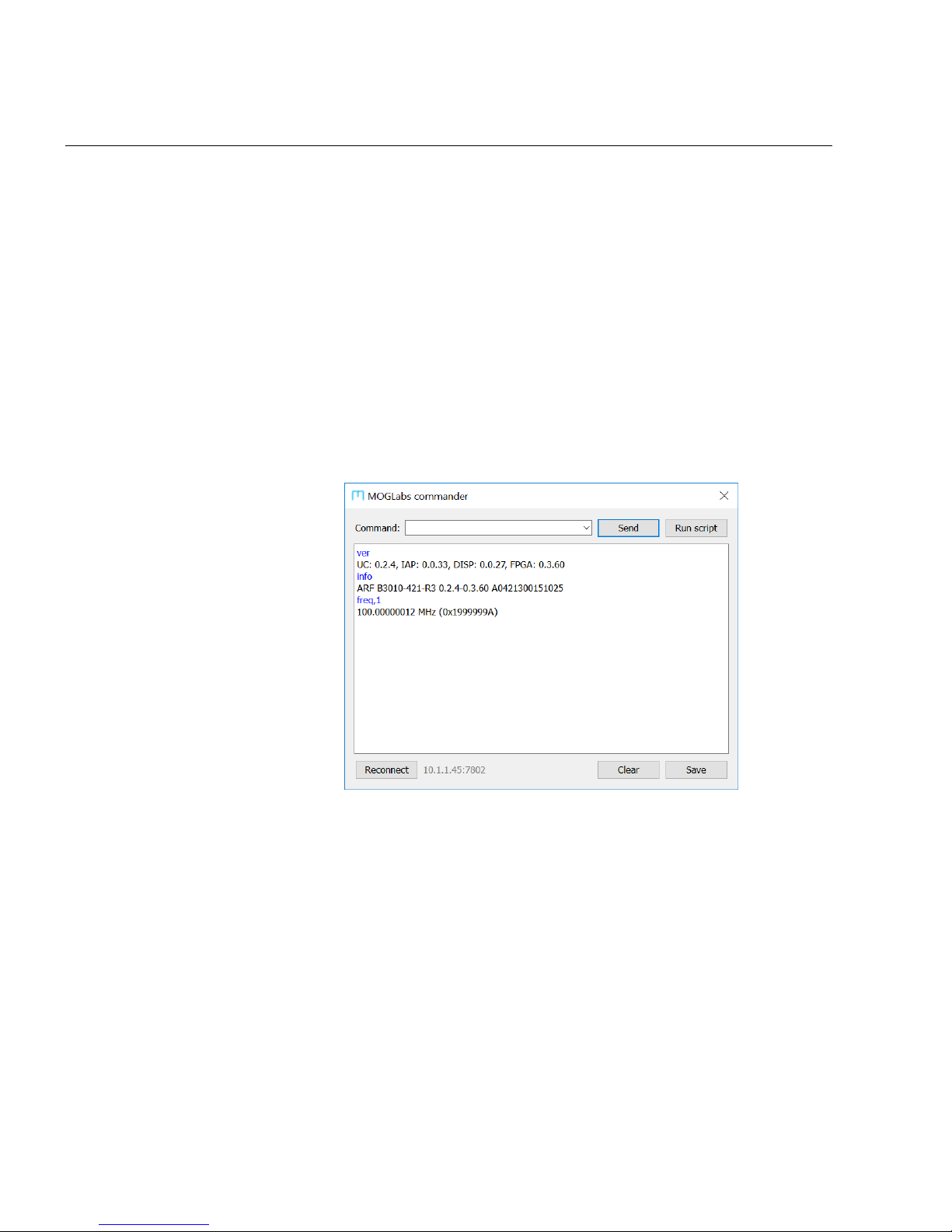
responses (Figure 3.1).
Figure 3.1: The mogcmd application, showing successful and unsuccessful
commands and queries.

3.2 TCP/IP 13
3.2 TCP/IP
When ethernet is connected, the ARF will attempt to obtain an IP
address by DHCP. If DHCP fails, an internally defined address will
be used. In both cases, the address will be shown on the device
display (for example, 10.1.1.190:7802), showing the address and
port number for communicating with the device.
3.2.1 Changing IP address
Depending on your network settings, you may need to manually
change the IP address. This is most easily done by connecting via
USB and using mogrf to configure the device IP settings (4.3.2).
Another approach is to temporarily reconfigure a computer to have
an IP in the same subnet as thedevice, then reconfigure the device
using mogcmd as follows,
1. Connect the ethernet directly to a computer ethernet socket,
not via a network switch or hub.
2. Configure the computer network settings to have an address
in thesameaddressspace astheARF.Typically youwill need
to temporarily assign the host computer an IP address in the
same subnet, such as 10.1.1.189.
3. Connect to the device using mogcmd and issue the following
commandstoenter“staticIP”modeandconfigurethegateway,
set,dhcp,0
set,ipaddr,"192.168.1.100"
set,ipgw,"192.168.1.1"
reboot
4. Wait for the restart and check the IP address on the screen.
5. Revert the IP address of the host computer.
6. Connect the ARF and host computer to the same network and
check the host can connect to the device’s new IP address.

14 Chapter 3. Communications
3.3 USB
The ARF/XRF can be directly connected to a host computer using a
USB cable (type A-male). The device will appear as a Virtual COM
port - a fast serial port that behaves like an RS232 connection.
The required STM32 Virtual COM Port Driver (VCP) device driver is
available from the MOGLabs website for the WindowsTMoperating
system. After installingthe driver,theARF/XRF willappearasanew
COM port on the machine.
To determine the port number of the device, go to Device Manager
(Start, thentypeDevice Manager into the Searchbox). You should
see a list of devices including “Ports” (Figure 3.2).
Thedevicecan beidentified asa COMport withthe followingname,
STMicroelectronics Virtual COM Port (COMxx)
where xx is a number (typically between 4 and 15). In the example
above, the device was installed as COM4.
Figure 3.2: Screenshot of Device Manager, showing that the ARF can be
communicated with using COM4. The port number might change when
plugging into a different USB port, or after applying a firmware update.

3.3 USB 15
Note that if the port appears in Device Manager with a different
name, then the driver was not successfully installed. If this occurs,
disconnect the device from the host computer, reinstall the VCP
driver, then reconnect the USB cable.

16 Chapter 3. Communications

4. MOGRF host software
The mogrf software package provides a simple user interface to
the basic behaviour of ARF/XRF devices, with the ability to issue
commands, run scripts, control tables, and apply firmware updates.
Please note: The software described in this section is designed to
workwiththemostrecent firmware,whichmayrequire youtoinstall
a firmware update (see Appendix B).
4.1 Device discovery
Upon starting the application, a device discoverer (Figure 4.1) is
initiated. This program scans the USB ports of the host computer
looking for an ARF/XRF device, and then scans the local network
subnet. Starting the application is then as simple as selecting the
device to communicate with and clicking Connect. If your device is
not listed, recheck your connection and network settings.
If the network and/orfirewall does not permitdevice discovery, it is
Figure 4.1: Example of the Device discoverer window, showing that one
USB device and two networked devices were detected.
17
18 Chapter 4. MOGRF host software
possible to enter the IP address of the unit in the Device address
box and connect directly.
4.2 Device commander
The Device commander is an interactive terminal for issuing commands andqueries to yourARF/XRF deviceanddisplayingthe result
(Figure4.2). Thecommands acceptedby theunit andtheirfunctions
arelistedin AppendixC. Commandscanbe typedintotheCommand
box and are executed upon pressing ENTER. The window contains a
history of recently executed commands.
Figure 4.2: The Device commander window, which permits the execution
of individual instructions or of text files containing scripts.
Scripts are ASCII text files where each line corresponds to a com-
mand to beexecuted(see Appendix D). Clicking Run script triggers
stepwiseexecutionofsuchascript, wherethe successofeachstatement is checked before executing the subsequent line. If an error
occurs, execution of the script is aborted and an error message is
displayed.
Ifthedevice isrestarted orthe connectionis lost,clicking Reconnect
will attempt to reestablish communication.

4.3 MOGRF main window 19
4.3 MOGRF main window
The main window of mogrf is shown below. The two channels are
displayed side-by-side, with information and controls that depend
on the current operational mode of each channel.
Figure 4.3: The main window of mogrf, showing Channel 1 in normal
(NSB) mode and Channel 2 in simple table (TSB) mode.
The main features of the application are as follows:
1. Currentoperationalmodeofthechannel. Clicktochangemode
by selectingfroma list. Note that “advancedtable mode”will
only appear on XRF units.
2. Current frequency,amplitude andphaseinNSB mode. Changing the value immediately updates the output.
3. Controlsareprovidedforspecifictable-modefunctionality. TablescanbeexchangedwithinternalFLASH memory,oruploaded/downloaded from thehost machinein binaryor CSV format
(§8.5). Tableexecutioncanbe startedorstopped,auto-restart
configured (§8.6), anda graphicalviewer is providedfor table
visualisation in TSB mode (§4.4).

20 Chapter 4. MOGRF host software
4. Channel output can be controlled by enabling only the RF
switch(signal),RFamplifiers(power)orboth(421-series only).
5. Options to enable external TTL control of the channel output
using the OFF input on the DB15 connector (see §7.5).
6. Current channel status. Includes whether any modulation options are enabled (both frequency and amplitude modulation
are enabled in this example) and the current execution status
in table mode.
7. Click Query tomanually updatethedisplayedstatus information. Usefulforreflecting changescaused bydevice commands
or front-panel input.
8. The status bar contains diagnostic information about the unit
and connection.
4.3.1 File menu
Device command Starts the Device commander (§4.2) for interactive execution of in-
structions to control the device.
Upload firmware Startsthe firmwareupdate applicationtouploadandinstallupdates
on the device. The procedure for applying firmware updates is described indetail inAppendix B. It is stronglyrecommended tomake
a backup of device settings (Settings→ Download settings) before
commencing an update.
Upload table Upload a previously downloaded binary table to FLASH memory,
which can be subsequently loaded into either channel. Note that
binary compatibility between firmware revisions is not guaranteed,
and it is recommended that all tables be generated and stored in
ASCII (human-readable) form.
4.3.2 Settings menu
Ethernet Allowsconfigurationofnetworkconnectionsettings(IP address,mask,
gateway and port). Particularly useful for configuring the network

4.3 MOGRF main window 21
settings over USB. Note that changing the Static IP only has an
effect if DHCP is disabled, or if DHCP name resolution fails.
Figure 4.4: Ethernet configuration interface.
Notethatchanging theethernetsettingswillrequire theapplication
toberestarted, andmay alsorequirethedeviceto berebooted. The
port shouldbe unchangedat7802 toensure thatthe mogrf suiteof
programs can continue to communicate with the device.
Modulation The ARF/XRF supports a wide variety of modulation options, which
can be configured from this interface (Figure 4.5). Individual modulation types can beenabled/disabled and their gainsadjusted. See
chapter5forinformationaboutthepossiblecombinationsofsettings.
Synchronisation Configures the channel synchronisation feature, detailed in §8.8.
MOD Out Select a monitoring signal to output on the MOD OUT connector on
therearpanel. Potentialsignalsare describedin thedocumentation
for the MOUT command.
Download settings Downloads configuration and calibration data from the device and
stores it in a file for backup purposes. It is strongly recommended
to download settings before applying firmware updates.

22 Chapter 4. MOGRF host software
Figure 4.5: Modulation settings interface,showingthat simultaneousFM
and AM is enabled on Channel 1, with high bandwidth on AM. PID is
disabled but constants have been set.
Upload settings Restore previously downloaded settings to the unit.
4.3.3 Help
Diagnostics Queries the unit for diagnostic information, which may be useful in
assessing issues with the functionality of the ARF/XRF (Figure 4.6).
When encountering aproblem with the device,please run thediagnostics and click “save results”. Please send the resulting text file
and a description of the problem to MOGLabs for analysis.
About Displaysversion informationaboutthe mogrf toolkitand connected
ARF/XRF device, for support purposes.

4.4 Table viewer 23
Figure 4.6: Diagnostic information about the connected ARF unit, which
should be sent to MOGLabs for analysis if there is a problem with the
device.
4.4 Table viewer
In simple table mode (TSB mode), mogrf provides a viewer for inspectingboththe tableinstructionscurrentlyloadedinto eachchannel, aswell astheinstructionsstoredinFLASH memory(Figure 4.7).
This is beneficial for cataloguing the sequences in memory, as well
as for debugging sequences which have been generated by scripts
and uploaded to the device.
At present, the table viewer is only available for simple tables, but
may be extended in future to provide visualisation of advanced tables. Also, table viewer maynot work correctly overUSB due to the
reduced communication speed of the virtual COM port interface.
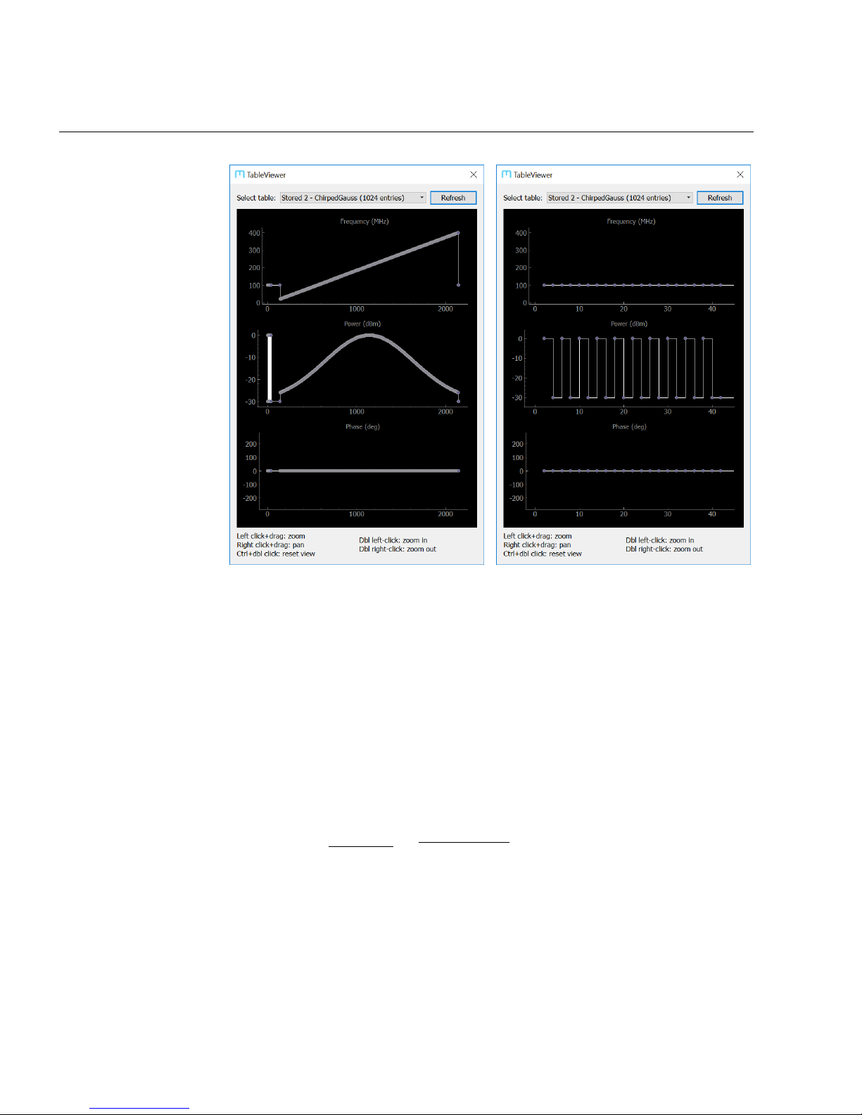
24 Chapter 4. MOGRF host software
Figure 4.7: Table viewer showing how the frequency,power and phaseof
a table stored in FLASH memory change across the sequence (left). The
example shown is a chirpedGaussian pulse,with a number ofrapid on/off
pulses at the beginning. Mouse controls allow zooming in on areas of
interest, such as the rapid pulses at the start of the sequence (right).
4.5 External I/O settings
TheARF/XRF providesextensivedigital I/Ocapability,andtheEXTIO
configurationwindow allowscontrollingtheseoptions, equivalentto
using theEXTIO command. The window isaccessible throughmogrf
by selecting Settings→ External IO from the menu. It displays the
current input and output state of the I/O pins on both the DB15
connector and the high-speed banks (chapter 7). This is beneficial
for checking that the I/O state matches what is expected, and that
any settings are correct for the desired application. In particular,
note that pins must be set to “AUTO” control to be used in table
mode.

4.5 External I/O settings 25
Features of the EXTIO configuration window (Figure 4.8) are:
1. Currentstateofthe inputpins ofthe DB15connector(notethat
SEQ is disabled on Rev2 units).
2. Options treat the OFF input on the DB15 connector as an interlock (“Latch” mode) or for direct control of the RF switch
(“Toggle” mode), as discussed in §7.5.
3. Current state of the DB15 digital output (“shutter”) pin, which
can be set manually or placed in “Auto” mode.
4. Analog monitoring signal currently output on the analog output pin of the DB15 connector.
5. Current state of the two high-speed banks. The banks are
disabled (black) on boot, and must be set to either Read or
Write modeon a per-banklevel. However, output pinscan be
individuallysetas“Auto”(tablemodeoutputs)or “Manual”by
right-clicking each indicator.
6. Mode of the associated high-speed bank. One of “Disabled”,
“Read” or “Write”. Note that “Read” mode is not availableon
Rev2 units.
Figure 4.8: External I/O configuration window, showing the current state
of inputs(yellow), outputs(green), table-modeoutputs (blue)anddisabled
outputs (black). Left-clicking on an output changes its state, and rightclicking brings up a menu of options.

26 Chapter 4. MOGRF host software

5. External modulation
The ARF/XRF supports external modulation of the RF through the
modulation input SMA connectors on the back-panel. Frequency,
amplitude and phase modulation ofthe RF are supported, anddualmodulation is possible for simultaneous FM/AM or FM/PM.
WARNING: The modulation inputs are nominally ±1V, and can be permanently
damaged by applying higher voltages. Ensure that modulation is disabled when
disconnectingtheback-panelSMA connectors,asfloatinginputscancauseunexpected
results. 50Ω termination is recommended when not in use.
5.1 Operational principle
Modulation is performed by digitising the analogue input signal,
whichisthen multipliedbythemodulationgain andaddedtotheinternal control valueassociated withthe particular modulationmode
(“frequency tuning word” for frequency, “amplitude scale factor” for
power or “phase offset word” for phase). Limits are applied to the
value to ensure that the power is always limited to the value set
with the LIMIT command.
TheDACoperates at62.5MS/s with12-bit resolution(±1V range),
anti-aliased with 7th-order filters for a measured 3-dB bandwidth
of 10MHz. Simultaneous modulation of two parametersis possible,
although one mode will have a reduced bandwidth (see §5.3).
Modulation is enabled/disabled with the MDN command. For example, to enable AM on channel 1, use the command MDN,1,AMPL,ON.
Modulation is not available in table mode.
Note: Since firmware v1.3.x, phase modulation uses the “FREQ” modulation input
SMA connector on the back-panel.
27

28 Chapter 5. External modulation
5.2 Modulation gain
The modulation gain, which controls the modulation depth, is set
using the GAIN command. The gain is specified as a signed 32-bit
integer(default0), ineither decimalorhexadecimal,withanegative
value inverting the modulation action1.
Note: Frequency modulation was changed in firmware v1.3.x to allow finer FM
control. It is now possible to modulate at either ∼Hz/V or ∼MHz/V, depending
on the gain. However, the gain used in earlier firmware revisions will need to be
multiplied by 32,768 for the same effect.
The range of gain values is shown in the table below. In principle,
modulation depth can also be decreased through the amplitude of
the input signal, but it is preferable to use the full ±1V dynamic
range to minimise discretisation error.
FM AM PM
Max gain (hex) 0x3FFF8000 0x3FFF 0xFFFF
Max gain (dec) 1,073,709,056 16,383 65,535
Step size 0.23Hz 0.006% Max 0.0055
◦
Max modulation 250MHz 100% Max 360
◦
Table 5.1: Gain ranges for different modulation modes.
Based on these values and ignoring discretisation and saturation,
the applied voltage causes the following modulation:
Frequency: df = (0.23 Hz/V)GfV
in
Phase: dφ = (0.0055◦/V)GφV
in
Amplitude (*): dA ≈
(14 V/V)GaV
in
for 421-models
(2.6 V/V)GaV
in
for 021-models
1
Negative hexademical values are represented using two’s complement.

5.3 Dual modulation: fast and slow modes 29
(*): This expression assumesa 50Ω load, and depends on the individual unit power calibration. The actual output amplitude respects
the maximum power limit set by the LIMIT command. The available
modulation depth depends on the difference between the current
output power (POW) and the predefined limit (LIMIT).
Similarly the gain required to achieve a desired modulation depth
at 1V input can be estimated as:
Gf=
1073709056
250 MHz
df, Gφ=
65536
360
◦
dφ, and GA=A0MA,
where MAis the amplitude modulation depth and A0is the initial
amplitude (returnedbythe POW commandasa hexadecimalnumber).
Examples: when using a ±1V modulation input,
• To change the frequency by ±1MHz, set the gain to
1073709056× (1/250) =4294836.
• To modulate the phase by ±45◦, set the gain to
65536× (45/360) =8192.
• To amplitude modulationby ±50%inan ARF421 at anaverage
RF power of+30dBm, usethePOW command todetermine that
the amplitude is 0x2000 = 8192, and set the gain to
8192× 0.5=4096.
5.3 Dual modulation: fast and slow modes
The ARF/XRF is capable of dual modulation, where the RF is either
simultaneously FM and AM or PM and AM modulated. However,due
toDDSinterfacelimitations,onlyoneparametercanbemodulatedat
full speedusing theparallel bus. The other parameteris modulated
on the serial bus at 1MHz.
The FMSPEED command allows selectionof which modulationparameter has higher bandwidth as shown in the table below.
The signal processing chain causes a propagation delay between
the modulation input and the RF output of approximately 500ns in

30 Chapter 5. External modulation
Command FM/PM bandwidth AM bandwidth
FMSPEED,1,FAST 10MHz 1MHz
FMSPEED,1,SLOW 1MHz 10MHz
Table 5.2: Effect of using FMSPEED to control modulation on Channel 1.
fast (parallel) mode, and <3µs in slow (serial) mode. Furthermore,
inducingastepchangewithslowmodulation(e.g. usingAMtoswitch
the output) may appear to have jitter of up to 500ns depending
on the delay between the change in the modulation input and the
subsequent DDS update.
Simultaneous FM and PM is notcurrently supported,as phasemodulation shares the “FREQ” modulation input.
5.4 Examples
5.4.1 Simple linear ramps
Listing 5.1 shows how to use the MOD OUT connector on the rear
panel to linearly ramping the RF amplitude and frequency simultaneously (Figure 5.1). Ensure that MOD OUT is connected to both
the FREQ1 and AMPL1 modulation inputs in parallel. Subsequently
increasing the AM gain results inclamping theamplitude to respect
the limit set by the LIMIT command (Figure 5.2).
# configure the channel
FREQ,1,60MHz
POW,1,0dBm
LIM,1,10dBm
ON,1
# connect MODOUT to FREQ1 and AMP1 mod in
MOUT,SHLRAMP
MDN,1,AMPL,ON,4000
MDN,1,FREQ,ON,30000
FMSPEED,1,SLOW
Listing 5.1: Simultaneous AM and FM

5.4 Examples 31
Figure 5.1: Demonstration of simultaneous AM/FM modulated RF (red)
when the modulation inputs are driven by the SLHRAMP monitor output
(blue).
Figure 5.2: Demonstration of high gain amplitude modulation showing
clipping at zero and the power limit set by the LIMIT command.

32 Chapter 5. External modulation
5.4.2 Comparison of fast and slow modulation
The example here shows the same amplitude-modulated waveform
usinga1Vppsinewaveat100kHz. WhenFMSPEED issetto FAST,the
amplitudeismodulatedusing theslowserial interfaceand theenvelope displayslargestepwise discretisation. However, whenFMSPEED
is SLOW, amplitude modulation uses the parallel interface and the
resulting envelope is smoother.
Figure 5.3: Comparison of slow (top) and fast (bottom) amplitude modulation for a 100kHz sine wave modulation input.

5.4 Examples 33
5.4.3 Phase modulation
In some applications, it is desirable to phase modulate one of the
channels by ±π, and use the other channel to demodulate the resulting signal usinga double-balanced mixer. This is achieved with
a 2Vpp modulation input with gain 0x7fff, or a 1Vpp modulation
input with gain 0xffff (Figure 5.4).
Figure 5.4: A 1Vpp, 10kHz triangle wave (blue) is used for phase modulation of CH1 and demodulated with an unmodulated CH2 at the same
frequency (magenta).
Notethatitmaybe necessary toadjustthephaseofone ofthechannels using the PHAS command to compensate for differential phase
delay in the signal paths.

34 Chapter 5. External modulation

6. PID stabilisation
In addition to external modulation, the ARF/XRF also implements
PID control loops which can be used in conjunction with an AOM to
perform intensityor frequencystabilisationof alaser. Each channel
has an independent PID controller, which acts to drive an “error
signal” provided to the modulation input towards zero.
EngagingthePID controllerinamplitudemodeadjuststheinstantaneous RF output power, which could be used to compensate for the
amplifier frequency responsewhen performingwide-band frequency
ramps, or to reduce the technical noise of a laser beam propagating through the AOM (“noise eating”). In frequency mode, the RF
frequency (and hence frequency shift of the diffracted order) is adjusted, allowing the beam to be frequency stabilised to a narrow
reference, such as a high-finesse cavity.
Note: As of firmware v1.3.0, theparameter thatthe PID controller acts upon must be
specified when enabling the control loop (e.g. PID,ENABLE,1,AMPL)
6.1 Signal conditioning
Upon engaging the PID controller, the associated modulation input
SMA connector on the back-panel is treatedas an “error signal” in-
stead ofa control voltage,andtheaction ofthe controller istodrive
this signal towards zero However, in applications such as intensity
stabilisation, it is desirable that the laserbeam power as measured
on a photodetector and isheld at a non-zero voltage. This requires
analog conditioning of the photodetector signal to subtract the desired set-point before being fed into the ARF/XRF input.
Furthermore, the modulation input used to digitise the error signal
has a ±1V range and12 bits ofprecision. To improve the response
35

36 Chapter 6. PID stabilisation
of the controller, it is often necessary to apply analog gain to the
error signal to make use of the full dynamic range of the ADC.
Suchsignalprocessingmust bedoneexternallyto theARF/XRF, with
bandwidth at least an order of magnitude greater than the desired
effective bandwidth of amplitude stabilisation. Care must be taken
to ensure that the signal fed into the ARF/XRF does not exceed the
±1V modulation input tolerance, such as with a clamping circuit.
For convenience, MOGLabs produces a signal-conditioning board
(B3120) available as an optional extra, which provides:
1. Manual offset adjustment, ±10V
2. Analog offset subtraction (e.g. from DAC output)
3. Variable analog gain
4. Monitor outputs for both photodetector and error signals
5. Output protection, to prevent exceeding ±1V.
6. 10MHz bandwidth
6.2 PID control loop
The ARF/XRF implements the feedback control via a standard PID
(proportional integral differential) function:
u(t)=Gkpe(t)+Gk
i
Z
t
0
e(τ)dτ +Gk
d
de
dt
,
where e(t) is the input error signal, u(t) is the feedback response,
and G is the overall modulation gain. The gain constants kp, ki, k
d
are floating-point values in the range [0, 1) which correspond to
proportional, integral and differential terms respectively. Typical
values are kp=0.03− 0.8, ki=0.01− 0.15 and kd=0.
The PID controller also has an anti-windup feature, which improves
recoveryfromasaturatedintegrator. Typicallythe anti-windupgain
should be equal to the integral gain, ka=ki.

6.3 Dual modulation with PID 37
WhenoptimisingaPID controlloop,itshouldbekeptinmindthatthe
achievableloopbandwidthislimitedby thepropagationdelayof the
entire signal processing chain, not just the modulation bandwidth.
This includes the impulse response of the AOM, photodetector and
signal-processing electronics, as well as the ARF/XRF.
6.3 Dual modulation with PID
It is possible to perform PID simultaneously with another form of
modulation enabled. For example, PID can be used to compensate
for the frequency response of RF components or the AOM when performing wide-band frequency modulation, as shown in Listing 6.1.
# enable FM on channel 1
MDN,1,FREQ,ON
GAIN,1,FREQ,0x3FFFF
# set PID gains and enable
PID,GAIN,1,P,0.1
PID,GAIN,1,I,0.01
PID,GAIN,1,D,0
PID,GAIN,1,A,0.01
PID,ENABLE,1,AMPL
# set FM to SLOW mode, allowing PID to be FAST
FMSPEED,1,SLOW
Listing 6.1: Simultaneous FM and PID intensity stabilisation example.
Limitations of the DDS interface mean that only one of PID and
externalmodulationcan beperformed atfullbandwidth(§5.3). Most
applications will benefit from using PID in “fast” mode, but some
applicationssuchascompensatingforthermaldriftinAOM diffraction
efficiency do not require high bandwidth and can be operated in
“slow” mode.

38 Chapter 6. PID stabilisation
6.4 Noise-eater implementation
A common application for PID controllers is optical noise eating,
whichtechnicalnoisearisingfrompowerfluctuationsinalaserbeam.
Figure 6.1 shows a typical configuration, where the intensityof the
undiffracted (zero-order) beam is stabilised as seen in Figure 6.2.
In this configuration, the AOM acts as a high-speed variable optical
attenuator, diffracting some of the light into the unused first-order
output. The transmitted optical power is measured with a photodetector, and the ARF/XRF controls the RF power in proportion to the
Photodetector
AOM
Laser
Stabilised
Oset
ARF/XRF
Beamsplitter
+
–
Error
Figure 6.1: Typical setup for optical power noise eater.
Time
Volts
Oset
Photodetector signal
ARF/XRF input error signal
1
2
3
4
5
Figure 6.2: Photodetector signal (magneta) and conditioned error signal
(blue) before and after activating noise-eater feedback (simulated). Note
that the DC offset must be subtracted during signal conditioning.

6.5 Example 39
measured optical power. If the measured power is too high, the RF
poweris increasedand morelightis divertedinto thediffractedoutput. This allows fluctuations in intensity to be suppressed, at the
expense of reducing the transmitted power slightly (typically 90%
transmission is achieved).
6.5 Example
The following example configures PID on Channel 1 for a particular
set of gain constants. Note that the gain constants must be tuned
for each particular implementation. It isrecommended thatthe gain
constants areadjusted usingthe mogrf host software(§4.3.2)while
monitoring the measured noise on a spectrum analyser.
# Setup channel 1 for PID noise−eater feedback
# set sample rate
PID,RATE,1,15.625
# set P, I, D, A gains
PID,GAIN,1,P,0.5
PID,GAIN,1,I,0.05
PID,GAIN,1,D,0
PID,GAIN,1,A,0.05
# set overall gain
GAIN,1,AMPL,100
# set frequency and power
FREQ,1,80MHz
POW,1,20dBm
# monitor u(t) on DAC output
PID,MON,1,output
# activate AMPLITUDE control
PID,ENABLE,1,AMPL
# check status
PID,STATUS,1

40 Chapter 6. PID stabilisation

7. Digital I/O
TTL digital inputs and outputs (0-5V) are provided on the ARF/XRF
through the DB15 connector on the rear panel, and the high-speed
bus (HSB). The inputs can be used as triggers and the outputs can
be controlled manually or using by table mode entries (§8.3).
Note: Digital inputs are pulled high, meaning that a disconnected
input pin is equivalent to supplying a TTL high to that input.
7.1 DB15 connector
The DB15 connector on the rear panel (Figure 7.1) provides both
analogue and digital output for monitoring, and digital inputs for
synchronisation purposes.
CHx-AOUT Pin 11 (Ch1), Pin 13 (Ch2)
Analogue outputs for diagnostics and monitoring, controlled by the
MOUT command. Notethatthechannel numberhererefers totheDAC
channel, which is not necessarily the same as the RF channel.
CHx-DOUT Pin 4 (Ch1), Pin 9 (Ch2)
TTL outputs that can be controlled manually or from table mode,for
example to activate a mechanical optical shutter or trigger another
device. This output has a rise time of 3us.
Note: Pin 9 is internally disconnected in some commercial DB15
cables. Please ensure your cable has pin 9 continuity when using
CH2-DOUT.
CHx-SEQ Pin 3 (Ch1), Pin 5 (Ch2)
Pin used for hardware triggering in table mode. When the table is
armed and a fallingedge is received, thetable begins executing. In
Rev2 units, this pin is not connected and the CHx-ON pin must be
used instead.
41

42 Chapter 7. Digital I/O
Pin Signal Type
1 CH1 OFF TTL in
2 CH1 ON TTL in
3 CH1 SEQ(*) TTL in
4 CH1 DOUT TTL out
5 CH2 SEQ(*) TTL in
6 CH2 ON TTL in
7 CH2 OFF TTL in
8 GND 0V
9 CH2 DOUT TTL out
10 GND 0V
11 CH1 AOUT ±2.5V
12 GND 0V
13 CH2 AOUT ±2.5V
14 GND 0V
15 GND 0V
Figure 7.1: Pinout of high-density 15-pin female D-style rear panel IO
connector. Pins marked (*) are not available in Rev2 units.

7.2 High-speed digital 43
CHx-ON Pin 2 (Ch1), Pin 6 (Ch2)
Driving thispin LOW inNSB mode instructstheFPGA toswitch ON
theRF signal(butnot theamplifiers). Shouldbe usedincombination
with OFF,ch,SIG. Has no effect if the RF signal is already enabled.
In Rev2 units, this pin also acts as CHx-SEQ when in table mode.
CHx-OFF Pin 1 (Ch1), Pin 7 (Ch2)
This input bypassesthe FPGA and directly turns the RF switch OFF
unless a TTL LOW is provided. Bypassing the FPGA provides an
extremely fast method for generating externally-controlled pulses,
as further discussed in §7.5.
This pin is disabled by default and must be enabled using the
EXTIO,ENABLE command. If enabled and the pin is disconnected,
the RF output will not turn on.
NotethatwhileCHx-ON andCHx-OFF appear toprovide similarfunctionality,theyhavedifferent timingproperties, anditis notintended
that both be used simultaneously. See §7.5 for more detail.
7.2 High-speed digital
InternalconnectorP1 providestwobanksof 8bitsofhigh-speeddigitalI/O.TheconnectoristypeOmronXF2M-3015-1A,30-way, 0.50mm
pitch. An FFC ribbon, Molex 0982660326 (150mm) or 0152660329
(200mm), can be threaded through a slot (left side) adjacent to the
connector.
Note: that the connector allows insertion of the FFC cable upside
down, effectively reversing the pin ordering.
An external breakout board such as the MOGLabs XSMA is recommendedwhen usingthehigh-speed bus,whichprovidesSMA connectorsfor eachpin andhasmatchedtracklengthsto ensureconsistent
propagation delay for all signals.
Each signal incorporates a series resistor (35Ω/10Ω Rev2/Rev3+)
and capability tosink and source 12mA. The associated driverchip

44 Chapter 7. Digital I/O
Pin Signal Pin Signal Pin Signal
1 3.3V 11 A4 21 GND
2 3.3V 12 A5 22 GND
3 3.3V 13 A6 23 B4
4 GND 14 A7 24 B5
5 A0 15 GND 25 B6
6 A1 16 GND 26 B7
7 A2 17 B0 27 GND
8 A3 18 B1 28 GND
9 GND 19 B2 29 GND
10 GND 20 B3 30 GND
Figure 7.2: High-speed digital IO connector (internal).
is a 74LVT2244 (Rev2, output only) or 74LVTH2245 (Rev3+, input or
output).
In Rev3+ devices, the FPGA can be configured to treat each of the
two banks of eight signals as either a bank of inputs or a bank of
outputs using the EXTIO,MODE command. That is, the pins can be
configured as entirely 16x digital output, entirely 16x digital input,
or 8x output and 8x input.
7.3 Configuration
The EXTIO command is used to control the behaviour of digital I/O.
Outputs can be set withEXTIO,WRITE, and queried with EXTIO,READ
when set to MANUAL control, or commanded by table mode entries
when set to AUTOMATIC control.
The table below shows the functionality available on the different

7.3 Configuration 45
pins. Pins in the high-speed bus can be addressed individually
(HSn) or collectively as a whole bank (HSBANK) in case multiple
outputs need to be changed simultaneously. HSB is short-hand for
HSBANK.
Function OFF ON/SEQ DOUT HSB HSn
Enable X - - X Disable X - - X Reset X - X X Mode X - - X Control - - X X X
Write - - X X X
Read X X X X X
Counter X - - - X
The different EXTIO commands are summarised below.
EXTIO,ENABLE EXTIO,ENABLE,ch,pin
Enable the functionality of the specified pin on the given channel
ch. If pin is HSB, the entire bank of pins is enabled.
EXTIO,DISABLE EXTIO,DISABLE,ch,pin
Disable the functionality of the specified pin.
EXTIO,RESET EXTIO,RESET,ch,pin
Resets the functionality of the specified pin to its default state.
EXTIO,MODE EXTIO,MODE,ch,pin,[mode]
Change the mode of the specified pin. If pin is HSB, then mode is
either READ or WRITE. If pin is OFF, then mode is either LATCH or
TOGGLE. If pin is disabled, it is enabled first.
EXTIO,CONTROL EXTIO,CONTROL,ch,pin,[mode]
Sets the control of the specified pin. The parameter mode is either
MAN[UAL] or AUTO[MATIC]. Pins must be set to AUTO mode to access

46 Chapter 7. Digital I/O
them intablemode. Ifpin is HSB andthe bankisnotin writemode,
the bank is changed to write mode first.
EXTIO,WRITE EXTIO,WRITE,ch,pin,value
Writethe specifiedvalue totheoutput pin. If pin is HSB,thenvalue
is an 8-bit number, whose bits correspond to the values to set on
the pins of that bank. Otherwise value can be one of ON, OFF, 1 or
0. If the pin is not set to MANUAL control, it is changed to manual
control first.
EXTIO,READ EXTIO,READ,ch,pin
Reads thespecifiedpin and returnsthe current stateoftheinput. If
pin is HSB, thenthe returnedvalueis an8-bit hexadecimalnumber.
EXTIO,COUNTER EXTIO,COUNTER,ch,pin,cmd
The FPGA implements independent digital counters on each supported pin. These counters can be individually started, stopped or
queried (see §7.6).
7.4 TTL switching
A versatile feature of the ARF/XRF is the ability to rapidly switch
the RF in response to an external input. This enables rapid pulsegeneration in synchronisation with other laboratory devices.
In high-power units, this is achieved by providing separate control
over the DDS output through controlof a fastRF switch, and control
over the amplifiers. The ON and OFF commands allow for individual
control, for example
ON,1 Turn on both signal and amplifiers (slow)
OFF,1,SIG Switch off signal only (fast)
ON,1,SIG Switch on signal only (fast)
ON,1,POW Turn onamplifiers only(slow)in preparation forTTL switching
The behaviour can also be controlled through the TTL inputs of the
DB15 connector which provide direct control of the RF switch and

7.4 TTL switching 47
allowtheoutputtobeswitchedwithminimaldelay. Thetworelevant
inputs are labelled CHx-OFF and CHx-ON (see 7.1). Both of these
inputs are active LOW, and have the following behaviour:
CHx-ON WhentheoutputisturnedOFF,pullingthispinLOW willswitch
the output ON (NSB mode only). Does not need enabling in
software, has no effect when disconnected.
CHx-OFF If CHx-OFF is enabled (see below), the RF output will not be
enabled unless this pin is pulled LOW. Note that with this
function enabled the RF output is disabled if the pin is dis-
connected.
The behaviour of the CHx-OFF input can be controlled as follows:
EXTIO,DISABLE,1,OFF
Disable the CHx-OFF input.
EXTIO,MODE,1,OFF,TOGGLE
Sets the CHx-OFF input to TOGGLE mode: the RF is switched
off whenever the input isheld HIGH and the output is switched
on whenever the input is held LOW. Can therefore be used for
generating rapid externally-controlled pulses.
EXTIO,MODE,1,OFF,LATCH
Sets the CHx-OFF input to LATCH mode: if the OFF input goes
HIGH, the output will be disabled and remain disabled. The
output can then only be re-enabled by taking the input LOW
andthen switching on the output viasoftwareorthe front-panel
button. This functionality can be used as part of an interlock
system.
EXTIO,ENABLE,1,OFF
Enable the CHx-OFF behaviour as configured by EXTIO,MODE.
Please notethatin Rev2 devices, theCHx-ON inputalso servesdualpurpose as a trigger in table mode.

48 Chapter 7. Digital I/O
7.5 External switching timing
Note: SomeRev2 andRev3 unitsmayrequireaminorhardwaremodification toachieve
the performance describedin this section. Please contact MOGLabs if you areinterested in performing this modification.
Thereareseveral approachesto generating pulsesusing anARF/XRF
in NSB mode (normal operation): using the TTL inputs on the DB15
connector,orusing amplitudemodulation(AM).Note thatwhengenerating pulses using AM, the input tolerance is ±1V, whereas the
TTL inputs are 5V-tolerant. Typical delays are shown in Table 7.1.
Method Transition Time
RF switch 25ns
RF switch 30ns
RF amp 2s
RF amp 2s
AM (fast) 500ns
AM (slow) < 3us
DB15-ON 2ms
DB15-OFF 40ns
Table 7.1: Typical on/off time delays for switching hardware components,
and for different methods of pulse generation.
Pulses can also be easily generated in a preprogrammed sequence
usingtable mode(see chapter8). Table modepulses onARF devices
arelimitedtoaminimumdurationof1µs,whereastheXRFiscapable
of the switch-limited timing above. Short pulses on ARF units can
only be generated in conjunction with the OFF input.
7.5 External switching timing 49
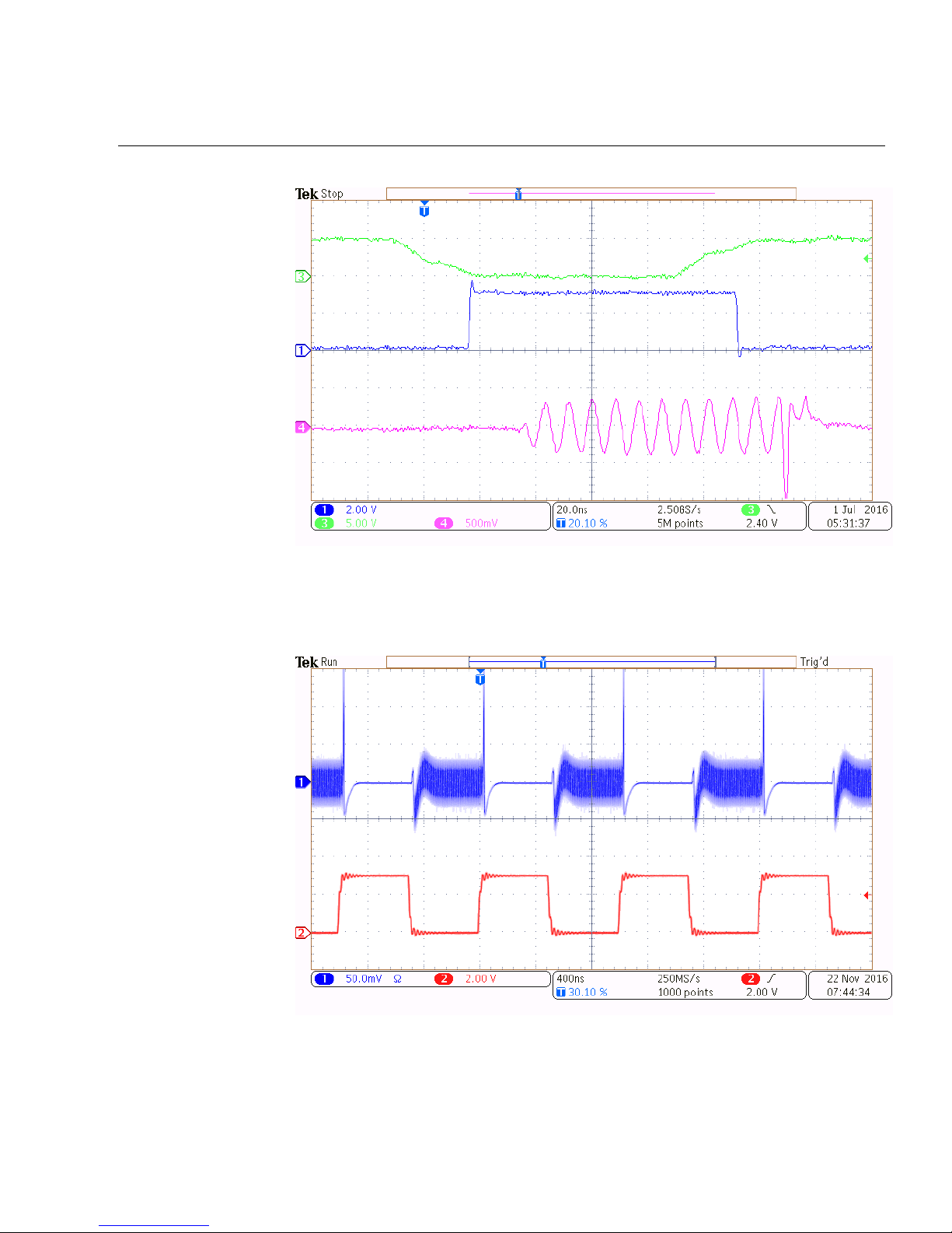
Figure 7.3: Modulation of RF output using the CHx-OFF input. Green is
TTL signal at the source; blue is the TTL signal at the RF switch (internal
to ARF); magenta is the RF signal.
Figure 7.4: Example ofpulse generation usingthe CHx-OFF input. Red is
TTL signal; blue is the RF signal.

50 Chapter 7. Digital I/O
7.6 Counters
Fastdigital counterscanbeaccessedforeachdigitalinputpin. XRF
devices can use these counters in advanced table mode (§9.4); ARF
devices can only use them manually in scripts. To use a counter,
the associated pin must be in READ mode and the counter function
activated. Themaximumcountrateonthehigh-speedbusis50MHz.
The syntax to control counters is EXTIO,COUNTER,ch,pin,command,
where command is one of the following:
READ, V[ALUE] Return the counter value as a 32-bit number
RESET, C[LEAR] Reset the counter value
E[NABLE] Activate counter and begin accumulating count
D[ISABLE] Deactivate counter but hold count value
H[IGH] Count while input is HIGH
L[OW] Count while input is LOW
R[ISING] Count rising edges
F[ALLING] Count falling edges
B[OTH] Count both rising and falling edges
The following example sets up a rising edge counter on HSB3 and
counts for 10ms.
EXTIO,MODE,2,HSB,READ
EXTIO,COUNTER,2,HS3,RISING
EXTIO,COUNTER,2,HS3,ENABLE
EXTIO,COUNTER,2,HS3,RESET
SLEEP,100 # wait approximately 100ms
EXTIO,COUNTER,2,HS3,READ # returns counts recorded

7.7 Examples 51
7.7 Examples
The following examples demonstrate how to configure and use the
external I/O pins. Note that pins must be set to MANUAL using the
EXTIO,CTRL command to be used for READ and WRITE.
These commands may be useful in executing scripts or diagnosing
experiments. For any application where timing is important, table
mode should be used.
EXTIO,CTRL,1,HSB,MAN
Set HSB1 to MANUAL mode, for use with READ and WRITE
EXTIO,WRITE,1,DOUT,1
Sets the CH1-DOut pin (DB15) to HIGH
EXTIO,READ,2,OFF
Reads the current state of the CH2-OFF pin (DB15)
EXTIO,MODE,1,HSB,WRITE
Set the entire first high-speed bank into write mode
EXTIO,WRITE,1,HS7,ON
Sets port 7 of HSB1 to TTL HIGH
EXTIO,WRITE,1,HSB,0x7
Simultaneously writes all pins in HSB1. Sets pins 0-2 HIGH
and pins 3-7 LOW
EXTIO,MODE,2,HSB,READ
Sets the entire second high-speed bank into read mode (only
available in Rev3+ models)
EXTIO,READ,2,HSB
Simultaneouslyreadall8-inputs ofthe secondHSB,andreturn
the result as an 8-bit number
EXTIO,READ,2,HS3
Read only port 3 of HSB2 (returns “ON” or “OFF”)

52 Chapter 7. Digital I/O

8. Simple table mode
Table mode performs sequential execution of up to 8191 instructions with precise timing. This enables generation of complicated
pulse sequences, customenvelope shapes, andautomated controlof
experiment sequences through digital I/O.
Therearetwo versionsoftable mode: simple tablemode(TSB mode)
which utilises the DDS serial interface, and advanced table mode
(TPA mode)thatutilises theparallelinterface. Advanced table mode
has increased functionality and improved timing resolution, as described in chapter 9, and is only available in XRF devices.
8.1 Operational principle
Atableis definedasanumber ofentriesthatdescribethe frequency,
amplitude and phase of the rf output at each step, as well as any
desired I/O. These are preloaded by the FPGA into a DDS “profile”,
so that when the sequence is executed the parameters are updated
instantaneously.
The speed of the serial interface limits the rate at which new instructions canbe loadedinto theDDS, sothe durationof eachtable
entry is discretised at 1µs.
1
Once the sequence has been defined using the TABLE,ENTRY commands, it is readied for execution using the TABLE,ARM command.
The table is checked for errors, and will fail if an incompatibility
is detected. For example, to use digital output, the associated pin
must be configured for AUTO control (§7.3).
Once the table is armed, execution is started by either a hardware
TTL trigger on the SEQ input
2
or using the TABLE,START command.
1
Advanced table mode (XRF) is capable of 16ns steps using the parallel bus.
2
On Rev2 units, the ON pin is used instead.
53

54 Chapter 8. Simple table mode
The phase-accumulator of the DDS is then reset and the table executes autonomously under FPGA control. This provides a very high
degree of reproducibility in terms of bothtiming of instructions and
outputoftheDDS generators,astheDDS phase accumulatorisreset
for every execution.
The table can be automatically restarted after completion by enablingtheTABLE,RESTART option, andexecutioncanbestopped midsequence using the TABLE,STOP command.
Each channelhas itsown independenttable, andthere areslots for
four distinct tables in non-volatile memory. Commonly-used tables
can then be stored on the device for later use. However, it should
be notedthat storedtablesmay becomeinoperableafter afirmware
upgrade and tables should be archived in human-readable form.
When a table is armed, the RF is switched on (including the amplifiers for 421-models), and upon completion of the table the final RF
state remains ongoing. If it is required that the output be disabled
when the table is complete, the final entry should set the power to
0x0 (zero amplitude, not 0dBm).
8.2 Defining table entries
Table entries can be directly set or queried using the TABLE,ENTRY
command. Once the entries have been set, the TABLE,ENTRIES command should beused toset thelength of thetable. Alternately, the
TABLE,APPEND command can be used to add an entry to the end of
the table and update the count automatically. Units are accepted
with relevant parameters.
TABLE,ENTRY TABLE,ENTRY,ch,num,[freq,pow,phas,dur,flags]
Configurethespecifiedtable entry. If onlych and num are given,the
current entry of the table is returned.
ch The channel to edit (1 or 2)
num The entry to edit (1 to 8191)

8.2 Defining table entries 55
freq Frequency to output during this step
pow Output power during this step
phas Phase of the RF for this step
dur Duration of this step (discretised at 1us)
flags A comma-separated list of flags, comprised of the following:
OFF Switch offthe RF signal for this step,disabling the output. Must
be repeated in subsequent steps for the signal to remain off.
TRIG Repeat the current instruction until a hardware trigger is re-
ceived, optionally specifying trigger source and edge (§8.3.3).
More advanced behaviour isavailable with the TABLE,LOOP command instead (§8.4).
IOxy Perform adigitalouputaction onpinx as specifiedbyy (§8.3.1).
Only one I/O operation can be performed in a given table entry.
IOSETx WritemultipleHSBdigitaloutputssimultaneously(§8.3.2)incon-
junction with an IOMASK flag.
IOMASKy Specifies which outputs should be controlled by IOSET (§8.3.2).
Thefollowing commandsarealsoprovidedto simplifyeditingtables
in memory. They take the same parameters as the TABLE,ENTRY
commandbutautomatically updatethetableentrycount asrelevant.
TABLE,APPEND TABLE,APPEND,ch,freq,pow,phas,dur,flags
Add the specified table entry to the end of the table and increment
the entry counter.
TABLE,INSERT TABLE,INSERT,ch,num,freq,pow,phas,dur,flags
Insert the specified entry into the table at the specified index, and
shift all other entries down.
TABLE,DELETE TABLE,DELETE,ch,num
Remove only the specified entry from the table.
TABLE,CLEAR TABLE,CLEAR,ch
Deletes the entire table from memory and resets any flags.
56 Chapter 8. Simple table mode
The example below shows basic operation of table mode using the
TABLE,ENTRY command. Entries are loaded in individually then the
total number is setwith TABLE,ENTRIES. The table is armedand executed usingTABLE,START.With TABLE,RESTART turned on,thetable
executes continuously.
The last instruction is held after the table completes, so it is good
practice to include a final instruction that sets the output power to
minimum.
# Example of table output
MODE,1,TSB
# Begin table
TABLE,ENTRY,1,1,100MHz,-10dBm,0,100
TABLE,ENTRY,1,2,100MHz,0dBm,0,100
TABLE,ENTRY,1,3,80MHz,-5dBm,0,100
TABLE,ENTRY,1,4,80MHz,-15.0dBm,0,100
TABLE,ENTRY,1,5,100MHz,-2.0dBm,0,100
TABLE,ENTRY,1,6,100MHz,0x0C00,0,100
TABLE,ENTRY,1,7,100MHz,0x0200,0,100
TABLE,ENTRY,1,8,100MHz,0x001,0,100
TABLE,ENTRIES,1,8
TABLE,START,1
Listing 8.1: Simple table mode demonstration.
Figure 8.1: Demonstration of Listing 8.1 on an ARF021.

8.3 Digital I/O 57
8.3 Digital I/O
Each entry inthe table cancontrol a singledigital I/O pin(§8.3.1),
or write multiple pins simultaneously (§8.3.2). However, pins must
be correctly configured using the EXTIO to be used in table mode:
inputs must beset to READ mode, and outputsmust be setto WRITE
mode with AUTO control.
8.3.1 Digital output
Digital output can be performed on any pin whichhas been configured for AUTO control using the EXTIO,CTRL command (§7.3). The
relevant flag is of the form IOxy, where x is the pin to use and y
the function to perform.
The pin can specified as:
D The digital output (DOUT) associated with this channel on the
DB15 connector
0-7 The specified pin of the high-speed bank with the same number
as this channel (A for CH1, B for CH2)
A0-A7 The specified pin of high-speed bank A (irrespective of channel)
B0-B7 The specified pin of high-speed bank B (irrespective of channel)
Both channelsare capableofaccessing thesameI/O pinsusingthe
second notation. It is up to the user to ensure that this does not
cause conflicts, particularly when loading a table from memory.
Available functions are listed below. Only the first letter is significant when specifying the command.
L[OW] Set the pin to output digital LOW
H[IGH] Set the pin to output digital HIGH
T[OGGLE] Switch the output level of specified pin
P[ULSE] Output a short pulse (∼ 500ns) on specified pin
Examples of I/O flags:

58 Chapter 8. Simple table mode
IO3H Set pin 3 of associated high-speed bank to output HIGH
IODT Toggle the output of the associated DOUT pin on the DB15
connector
IOA2P Output a short pulse on pin 2 of high-speed bank A
IOB1L Set pin 1 of high-speed bank B to output digital LOW
Theexamplebelow showshowtotoggleanoutput inthe high-speed
bank, resulting in the output shown in Figure 8.2.
MODE,1,TSB
# set HSB−A to output
EXTIO,MODE,1,HSB,WRITE
# set HSB pin A1 to AUTO mode
EXTIO,CONTROL,1,HS1,AUTO
# define table −− same frequency, five different amplitudes
TABLE,ENTRY,1,1,100MHz,0x200,0,2
# next entry sets pin 1 high
TABLE,ENTRY,1,2,100MHz,0x600,0,2,IO1H
# 2us later, set pin 1 low
TABLE,ENTRY,1,3,100MHz,0x1000,0,2,IO1L
TABLE,ENTRY,1,4,100MHz,0x1400,0,2
# create 500ns pulse
TABLE,ENTRY,1,5,100MHz,0x2000,0,2,IO1P
TABLE,ENTRY,1,6,100MHz,0x200,0,2
# toggle pin 1 (from low to high)
TABLE,ENTRY,1,7,100MHz,0x600,0,2,IO1T
TABLE,ENTRY,1,8,100MHz,0x1000,0,2
# toggle pin 1 again (i.e. from high to low)
TABLE,ENTRY,1,9,100MHz,0x1400,0,2,IO1T
TABLE,ENTRY,1,10,100MHz,0x2000,0,2
TABLE,ENTRIES,1,10
Listing 8.2: Simple example showing digital output in table mode.
8.3.2 Simultaneous digital output
As of firmware v1.3.0, it is possible to simultaneously set multiple
digital outputs in a single table instruction using the IOSET and
IOMASK flags. Both instructions take a 16-bit number, where each

8.3 Digital I/O 59
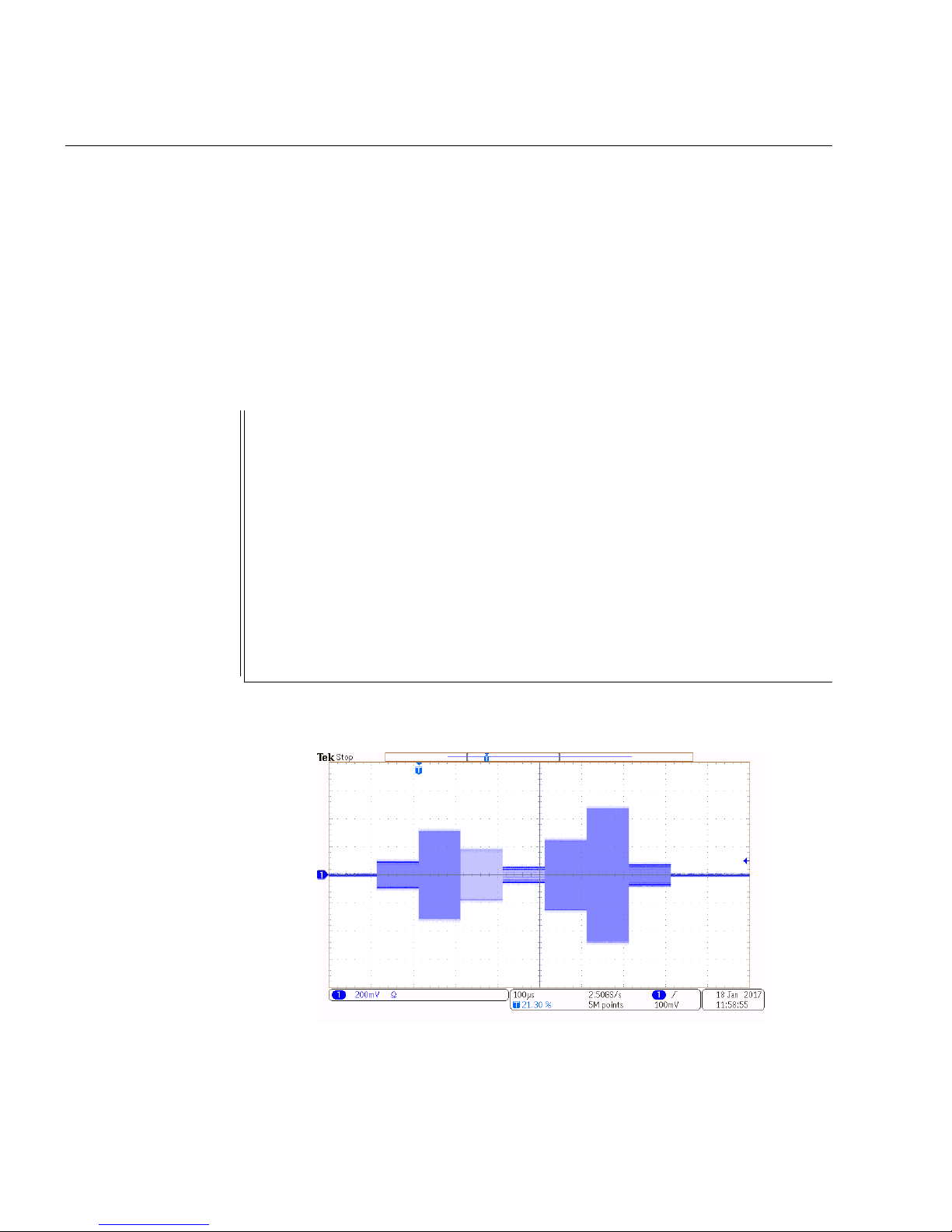
Figure 8.2: Example of table mode, showing changing RF output (blue,
lower trace) and synchronised TTL output (red, upper trace) generated by
the example in Listing 8.2.
bit corresponds to a pin of the high-speed output banks. If a bit is
set in the IOMASK value, then the corresponding value of IOSET is
written to that pin, overwriting any previous value. This allows all
pins ofboth high-speedbanksto bechangedin eachtable entry,or
only a subset of the pins. Table 8.1 demonstrates an example that
simultaneously writes 5 pins of bank A and 4 pins of bank B.
Bank B Bank A
Bit 16 15 14 13 12 11 10 9 8 7 6 5 4 3 2 1
IOSET 0 0 1 0 1 1 1 1 1 0 0 1 0 0 1 1
IOMASK 0 1 0 0 1 1 0 1 1 1 1 0 1 0 1 0
Outcome - 0 - - 1 1 - 1 1 0 0 - 0 - 1 -
Table 8.1: Example of simultaneous output using IOSET0x2F93 and
IOMASK0x4DEA. Only the 9 pins corresponding to bits set in IOMASK
are affected by the command, with “-” denoting no change.
If IOMASK is not specified, the value 0xFFFF is assumed and all HSB

60 Chapter 8. Simple table mode
outputs are written at once. Care must be taken when running two
tables simultaneously to ensure that the same pin isn’t being written to simultaneously by both tables, which canresult in undefined
behaviour. For reference, IOMASK0x00FF will only write to bank A,
and IOMASK0xFF00 will only write to bank B. It is recommended to
encode values in hexadecimal to improve readability.
Where only a few outputs need to be combined, it is possible to
chain togethermultipleIOxH and IOxL flagson thesametableentry
to avoid needing to construct the mask word. For example, the
following set of output flags could be used,
IOA3H, IOA4L, IOB1H,
which is equivalent to
IOSET0x0208, IOMASK0x0218,
but has improved clarity.
Note: MultipledigitaloutputmodecannotbeusedincombinationwithLOOP orTRIG.
8.3.3 External trigger
The TRIG flag indicates that the current instruction should be repeated until a hardware trigger is received. The source and trigger
condition can also be specified using the syntax TRIGxy where x is
the pin (§8.3.1) and y is the condition, which is one of the following:
H[IGH] Terminate loop if logic HIGH is detected
L[OW] Terminate loop if logic LOW is detected
F[ALLING] Terminate loop if a falling edge is detected
R[ISING] Terminate loop if a rising edge is detected
Inthisinstancethepin“D”refersthetheexternalinput on theDB15
connector (either the SEQ input on Rev3+, or the ON input on Rev2).
If no pin or condition is specified, the default is a falling trigger on

8.3 Digital I/O 61
the DB15 external input (equivalent to TRIGDF).
The trigger behaviour is to repeat the current instruction until a
trigger is received. Thus if the trigger condition is met during the
instruction period, execution will not immediately proceed to the
next instruction but rather complete the duration of the instruction
first. Hence thedurationof aTRIG instructionshould beas small as
possible to ensure rapid response to the trigger input.
Once atableis armedwiththeTABLE,ARM command itwill automatically begin executing upon a falling external trigger on the DB15
input; inthis instanceit isnot necessarytospecify theTRIG flag on
the first table entry.
If a trigger is not received, the TABLE,STOP command must be used
to abort operation.
Examples of trigger flags:
TRIG Continue on a falling edge on the DB15 input
TRIGDH Continue if the DB15 input is logic HIGH
TRIGA3R Continue on a rising edge on high-speed pin A3
The examplebelow shows howto use the TRIG flag, and the typical
observed behaviour.
# set table mode
MODE,1,TSB
# ready HSB1 for output
EXTIO,CTRL,1,HSB,AUTO
# create table
TABLE,CLEAR,1
TABLE,APPEND,1,100,5,0,10
# wait for trigger on next instruction
TABLE,APPEND,1,100,10,0,1,IO1T,TRIG
TABLE,APPEND,1,100,-5,0,10
TABLE,APPEND,1,100,-30,0,3,IO1L
# ready table for execution
TABLE,ARM,1

62 Chapter 8. Simple table mode
Figure 8.3: Demonstration ofwaiting foratrigger withinatable sequence.
The second table entry is repeated until a falling edge in the trigger
(magenta, top) is detected. The digital output (red, bottom) is toggled
several times showing the instruction being repeated.
8.4 Loops and triggers
Loops can be configured to simplify the generation of pulse sequences, or to wait for a hardware trigger to synchronise with external devices.
TABLE,LOOP TABLE,LOOP,ch,source,dest,condition
Setthetabletoloopbetweenthesource anddest instructionsuntil
the condition is satisfied. If source and dest are the same, or if
dest is 0, then the table effectively “holds” the instruction.
source and dest can be negative numbers, which are then taken as
offsets. If source is negative, it is taken as an offset from the end
of the table (requires TABLE,ENTRIES to be set). If dest is negative,
it is taken as the offset from the source. This is particularly convenient when using the TABLE,APPEND command, which updates the
TABLE,ENTRIES value after every call.

8.4 Loops and triggers 63
The condition canbe anintegerin therange[1, 4095], corresponding to the number of times to execute the loop, or a hardware descriptorflagoftheformIOxy,indicatingtheloopshouldberepeated
untilthedigitalinputpin x exhibitsbehaviour y,asdescribedbelow.
The pinsyntaxis describedin§8.3.1, althoughthe pin“D”refers to
the trigger input of the DB15 connector3. The behaviour y is one of
the following options:
H[IGH] Terminate loop on logic level HIGH at the loop instruction
L[OW] Terminate loop on logic level LOW at the loop instruction
F[ALLING] Terminate loop on falling edge during the loop
R[ISING] Terminate loop on rising edge during the loop
The TRIG flag of the TABLE,ENTRY command is short-hand notation
for TABLE,LOOP using the IODF condition.
Loops are subject to the following restrictions:
• Nested loops are not supported
• The TABLE,LOOP command can only be used after the source
entry has been defined
• The first and last entries of the table cannot be the source of
a LOOP command, but can be the destination
• Loop conditions are checked at the start of the instruction
• All loops will execute at least once, even if the condition is
met when the loop is first entered
• Insimpletablemodetheremustbeaminimumof4 tableentries
between consecutive LOOP instructions.
The examplebelow shows how todefine a loop witha fixed number
of iterations. Theloopcounteris4, soinstructions1–3areexecuted
a total of 5times (Figure 8.4). Since the final instruction cannot be
3
CHx-SEQ for Rev3+ and CHx-ON for Rev2.

64 Chapter 8. Simple table mode
aloopsource, a“dummy” instructionisaddedtotheend,whichalso
turns off the RF.
TABLE,CLEAR,1
TABLE,ENTRIES,1,4
TABLE,ENTRY,1,1,100MHz,0dBm,0,1us
TABLE,ENTRY,1,2,100MHz,-5dBm,0,4us
TABLE,ENTRY,1,3,100Mhz,-10dBm,0,2us
TABLE,LOOP,1,3,1,4
TABLE,ENTRY,1,4,100MHz,-30dBm,0,1us
Listing 8.3: Demonstration of a simple loop
Figure 8.4: Demonstration of a simple loop.
An alternate way of specifying the LOOP instruction in the above
example is
TABLE,LOOP,-2,-3,4
astheTABLE,ENTRIES was alreadyset to4, sosource -2corresponds
to entry 3, and the destination is 3 instructions earlier. However,
this form is only recommended when using TABLE,APPEND.

8.5 Upload and download 65
8.5 Upload and download
The host software mogrf provides convenient functionality that enables uploadanddownload oftablesin bothbinaryand CSV format.
This simplifies handling of tables, and allows simple generation of
sequences fromscripting languageslike matlab orpython, andthe
human-readable structure simplifies trouble-shooting.
Binary format enables direct upload of table data into non-volatile
memory and is provided for fast back-up purposes. The internal
binary representation of tables is likely to change between minor
firmware revisions due to the implementation of new functionality
that makes old binary tables incompatible with new firmware. It
is strongly recommended that all tables be stored in ASCII (humanreadable) format forlong-term storage. An example ofthis formatis
shown below.
100 MHz , -5 dBm , 0 deg , 10 us
150 MHz , 0 dBm , 90 deg , 2 us , I O DH
80 MHz , 5 dBm , 0 deg , 1 us , T R IG
100 MHz , 0 dBm , 0 d e g , 5 us
Listing 8.4: Example of table mode CSV file for use with mogrf.
A distinction should be made between CSV tables and scripts. In
this context, CSV tables contain only the table instructions directly,
whereas scripts may contain arbitrary sequences of command for
the device. Listing 8.4 demonstrates the format of a CSV table. The
intention is that such files are more easily generated by scripting
languages (such as matlab or python).
MODE,1,TSB
TABLE,CLEAR,1
TABLE,ENTRIES,1,4
TABLE,ENTRY,1,1,100MHz,-5dBm,0deg,10us
TABLE,ENTRY,1,2,150MHz,0dBm,90deg,2us,IODH
TABLE,ENTRY,1,3,80MHz,5dBm,0deg,1us,TRIG
TABLE,ENTRY,1,4,100MHz,0dBm,0deg,5us
Listing 8.5: Script equivalent to Listing 8.4.

66 Chapter 8. Simple table mode
8.6 Re-arm and restart
The microcontroller can be instructed to automatically re-arm the
table after a successful execution using the TABLE,REARM command.
Thisautomaticallyprepares thetable forexecutionfromeither hardware or software trigger once execution has finished.
Furthermore, the table can be repeated continuously by enabling
the TABLE,RESTART option. This option instructs the microcontroller
to re-executethe table onceit has finished. The finaltable entry is
held until the table is restarted, and there can be a variable delay
betweentablecompletion andrestart dueto variablemicrocontroller
workload.
Typically the time between a table completing and subsequently
restarting is ∼ 120µs. If this delay is unacceptable, an alternative
is tospecify aloop back tothe beginningof thesequence usingthe
TABLE,LOOP command which will repeat the table with no delay.
Asthelasttable entrycannot bea loop, a“dummy”instructionneeds
to be appended, as in the example below. This table will terminate
after 4096 executions; an alternative is to specifyto repeat untilan
external trigger that is never provided, which will loop forever.
# ...
# Instructions that define the CH1 table
# ...
# ...
# add a LOOP to the last instruction (−1) that goes back to the first (1)
TABLE,LOOP,1,-1,1,4095
# last instruction cannot be a loop −− add a dummy instruction
TABLE,APPEND,1,100MHz,-30dBm,0,1us
Listing 8.6: Demonstration of restarting CH1 table using a loop.

8.7 Linear ramps 67
8.7 Linear ramps
It is often desirable to linearly ramp a parameter without having
to specify the individual table entries manually. The TABLE,RAMP
command provides a convenient way to generate such ramps.
TABLE,RAMP TABLE,RAMP,ch,param,start,stop,duration,count
Appends table entries to the channel ch that linearly ramp param
from start to stop in count steps, with each step lasting for the
given duration. param is one of FREQ, AMPL or PHAS. The start and
stop valuescan bespecified withrealunitsasappropriate forparam.
The values of the other parameters are taken from the last entry
in the table. In simple table mode, count entries are generated,
whereas in advanced table mode only 3 entries are required.
For example, the command TABLE,RAMP,1,FREQ,80,100,100us,2000
inTSB modewill generate2000 tableentries correspondingto afrequencyrampthat sweepsthe RF frequencyfrom 80MHzto100MHz
inatotaltimeof200ms (eachstep being10kHzandtaking100us).
Thecommandcanalsobeused tospecify piecewise-linearenvelopes
using the AMPL parameter, such as in Listing 8.7 resulting in the RF
output in Figure 8.5.
MODE,1,TSB
# clear the table
TABLE,CLEAR,1
# define initial conditions (i.e. freq and phase)
TABLE,APPEND,1,80MHz,-30dBm,0deg,1us
# ramp power from −30dBm to 0dBm in 100us, then down again
TABLE,RAMP,1,POW,-30,0,1us,100
TABLE,RAMP,1,POW,0,-30,1us,100
# should now have 201 entries
TABLE,ENTRIES,1
# arm the table
TABLE,ARM,1
Listing 8.7: Example using TABLE,RAMP to create an envelope.

68 Chapter 8. Simple table mode
Figure 8.5: Output generated by Listing 8.7 showing linear ramps in
amplitude.
The ramp functionality can also be applied to frequency or phase.
Listing 8.8 shows how multiple TABLE,RAMP commands can be used
to execute asequence of slowfrequency ramps thatcan bewatched
on a spectrum analyser. A graph of the corresponding frequency of
the RF over time is shown in Figure 8.6.
MODE,1,TSB
TABLE,CLEAR,1
# set initial conditions
TABLE,APPEND,1,80MHz,0dBm,0,1us
# define first ramp
TABLE,RAMP,1,FREQ,70,80,1m,1000
# append a pause
TABLE,APPEND,1,80,-5dbm,0,1s
# append second and third ramps
TABLE,RAMP,1,FREQ,80,75,5m,200
TABLE,RAMP,1,FREQ,75,85,2m,500
Listing 8.8: Example demonstratinguse ofTABLE,RAMP to create multiple
frequency ramps.

8.8 Synchronous table execution 69
0 1 2 3 4 5 6
Time (s)
70
72
74
76
78
80
82
84
86
Frequency (MHz)
Figure 8.6: Frequency ramps achieved by chaining together RAMPFREQ
commands in TSB mode.
8.8 Synchronous table execution
When operating both channels in table mode, it is possible to synchronisethetwochannels. This synchronisationoccursbothatFPGA
level (sothatthe tableentriesare steppedthroughsimultaneously),
and at theDDS level (so that the RF generated by thetwo channels
remain in phase).
Thisfeatureisactivated byissuingthecommand TABLE,SYNC,1. This
configures CH1 asthe “master” andCH2 as the“slave”, such thatthe
CH2 DDS derives its clock from the CH1 DDS for phase stability.
Onceenabled, CH2 cannotbestartedindependentlyof CH1,and CH1
cannot be started unless CH2 has been armed. For this reason,it is
recommended to activate the auto-rearm feature on CH2 using the
command TABLE,REARM,2,1.
The feature must be deactivated using TABLE,SYNC,0 to run the tables independently, or to take one channel out of table mode. The
FPGA is also slightly slower (∼ 1µs) to respond to a start instruc-
tion (software or hardware trigger) insynchronous mode, as it must
prepare the each channel’s DDS for execution.
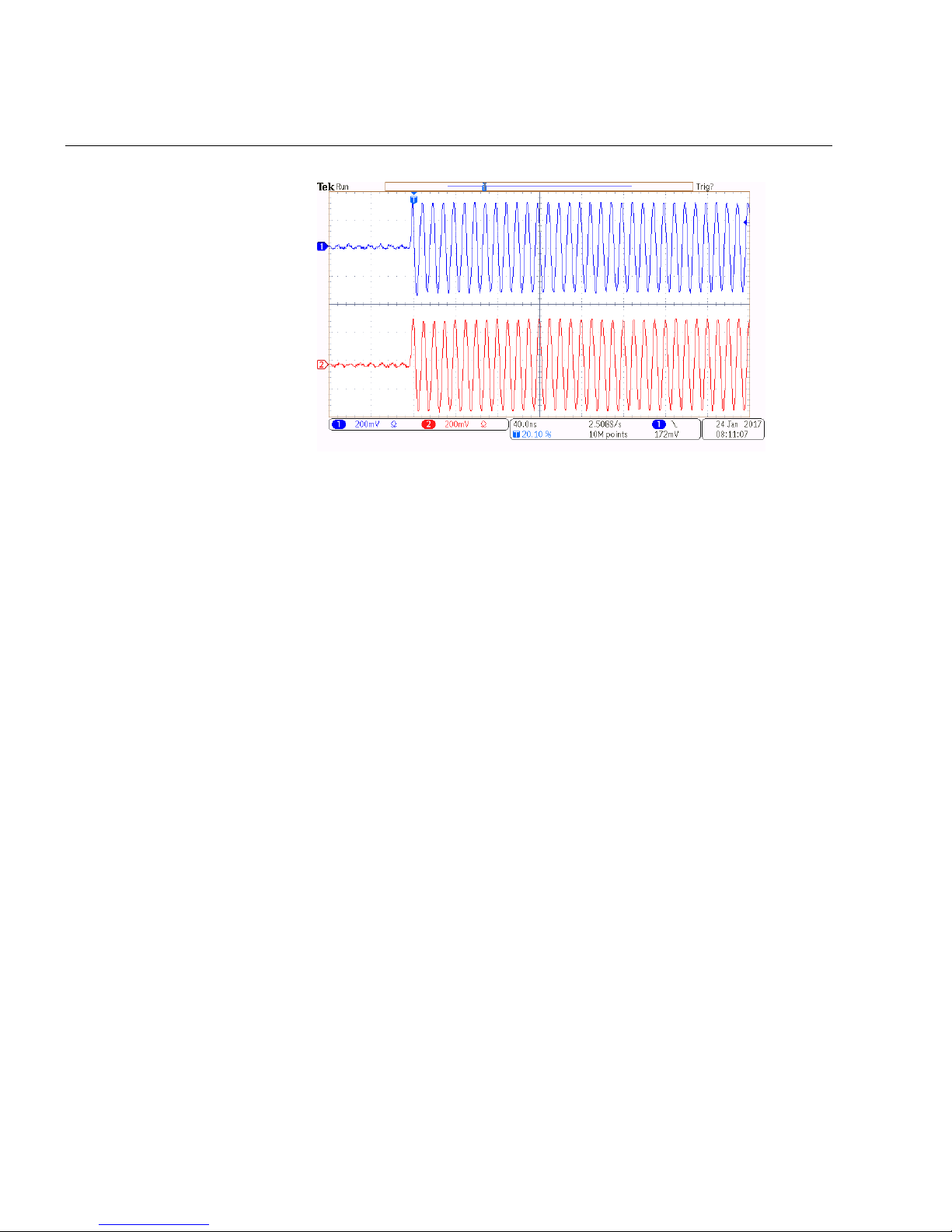
70 Chapter 8. Simple table mode
Figure 8.7: Exampleshowing thetwoRF outputswhen executingthe same
table synchronously on both channels. The RF remains in phase across
table instructions.
It is also possible to synchronise the DB15 triggers received by the
two tables. The two trigger inputs on the DB15 connector can be
hardwired together, but the FPGA can also be instructed to trigger both channels from the same input. This functionality can be
controlled by the TABLE,TRIGSYNC command.
This does not apply to the high-speed bus, as both tables can be
instructed to use the same input as a trigger regardless.

9. Advanced table mode (XRF)
TheXRF has access toan advanced table mode withincreasedfunctionality, flexibility and significantly faster execution than normal
(SIF) tablemode. Due to theaddedcomplexity,it isstronglyrecommendedthatusers befamiliar withsimple tablemodebeforereading
this chapter.
9.1 Operational principle
Advanced table mode performs table execution through the parallel interface (PIF) of the AD9910 DDS. This allows one parameter to
be updated at the maximum supported rate, currently 16ns per instruction. Due to limitations of the AD9910 DDS devices, only one
parameter can be modified via PIF, and the other parameters must
beupdatedattheslowerrate supportedbythe serialinterface(SIF).
There are therefore two kinds of instructions in advanced mode:
parallelandserial. Parallelinstructionsallowasingleparameterto
be updated rapidly, whereas serial instructions are preloaded into
the serial interface and then activated in a subsequent command.
This load/activate cycle allows changes to be made to the parallel
parameter without having to wait for the serial load to complete.
Advanced mode also supports a more extensive selection of loop
options, includingthe abilityto incrementthe parallelparameterfor
piecewise linear interpolation. This is advantageous for generating
smooth envelopes with only a few table instructions.
The FPGA supports I/O at the full update rate, but the rise-time
(particularly on the DB15 connector) must be taken into account.
The MOGLabs B3120 break-out board is recommended when using
the high-speed bus as it has matched track lengths to minimise
relative delay between the signals.
71

72 Chapter 9. Advanced table mode (XRF)
It should also be noted that the while the DDS outputs can be synchronised, the rf components following the DDS introduce a small
frequency-dependent propagation delay. However, this delay is
fixed for a given frequency, and can be calibrated in applications
where it is important. Such applications likely need calibration
anyway, due to propagation delay introduced by cables and other
external components.
9.2 Defining table entries
There aretwo formsof syntaxfor definingtable entries inadvanced
mode, corresponding to parallel or serial instructions. Before populating the table, the parallel parameter needs to be set using the
TABLE,XPARAM command, after which entries can be set for that pa-
rameter (syntax 1). A second format is provided for loading serial
commands, which is identical to simple table mode (syntax 2).
TABLE,XPARAM TABLE,XPARAM,ch,param,[fmgain]
Sets which parameter is to be controlled on the parallel interface.
Must be called before the table is populated with entries. The
parameteris oneof FREQ, PHAS,POW orAMPL. The parametersPOW and
AMPL are synonyms in this mode. Subsequent PIF table entries can
then modify this parameter. When entering FREQ mode, the fmgain
must also be specified (see §9.7).
TABLE,ENTRY
(1)
TABLE,ENTRY,ch,num,param,value,duration,flags
Setthe specifiedtable entrytochange param to thespecifiedvalue,
whileotherparametersremainunchanged. Duringnormaluse,param
should match the parameter set by TABLE,XPARAM, but some special instructions are available (§9.8). The duration of the entry is
rounded to the nearest multiple of 16ns, and the duration 0x1 can
be used to set the minimum possible duration. The same flags are
supported as in simple table mode (including TRIG and IOxy), with
some extra options as explained in this chapter.
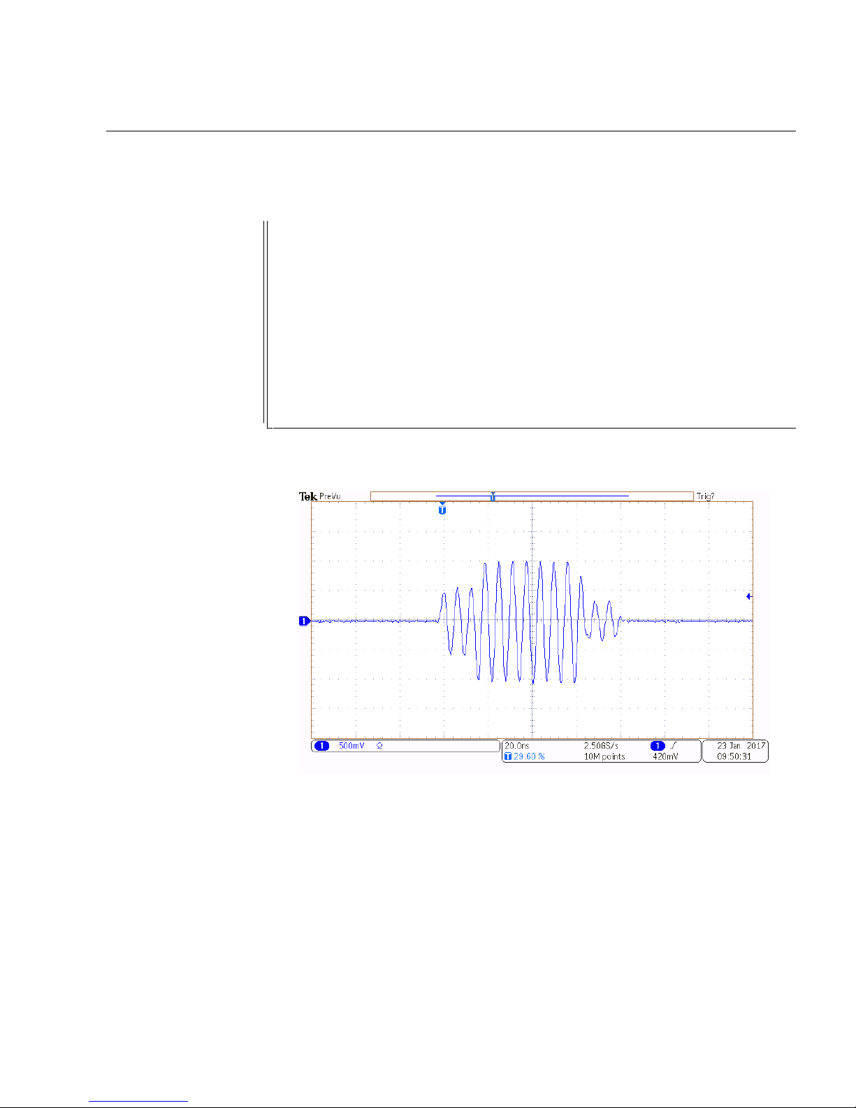
9.2 Defining table entries 73
The listing below demonstrateshow to set up advanced table mode
to control the envelope (amplitude) of the RF signal,
# enter fast table mode
MODE,1,TPA
# clear any table entries or settings
TABLE,CLEAR,1
# set amplitude (power) as the parallel parameter
TABLE,XPARAM,1,POW
# define a table
TABLE,APPEND,1,POW,5dbm,16ns
TABLE,APPEND,1,POW,10dbm,50ns
TABLE,APPEND,1,POW,0dbm,16ns
TABLE,APPEND,1,POW,-40dbm,16ns
Listing 9.1: Parallel instruction example in advanced table mode.
Figure 9.1: Output generated by Listing 9.1.
Parallel-mode instructions also provide functionality for piecewise
linear-interpolations,asdescribedin§9.6. Thisenablesthecreation
of smooth ramps without requiring a large number of instructions.
The functions TABLE,APPEND and TABLE,INSERT can also be used,
supporting either syntax.

74 Chapter 9. Advanced table mode (XRF)
It is anticipated that many applications will only seek to control a
single parameter, in which case only the parallel interface need be
used. However, a second command format is providedto simultaneously set all three parameters using the serial interface.
TABLE,ENTRY
(2)
TABLE,ENTRY,ch,num,freq,pow,phase,duration,flags
Defines a serial (SIF) instruction that updates all parameters using
the same syntax as simple table mode (§8.2), but the instruction
does not take effect immediately. The instructions are queued for
loadovertheserialinterfaceandmustbeactivatedbyasubsequent
table entry using the UPD flag. This ensures that the output only
changes in accordance with a table instruction.
The time between issuing the serial instruction and theupdate flag
mustbeatleast 960nsotherwise theDDS does nothave timeto load
theinstructions. However,anyflagsspecifiedintheinstruction(such
as digital output) will occur immediately.
The example below demonstrates howto queue and then activate a
serial instruction in advanced table mode.
# define a SIF entry using simple mode syntax
TABLE,APPEND,1,100MHz,5dbm,0,1us
# trigger the update to take effect
TABLE,APPEND,1,POW,0dbm,0x1,UPD
Listing 9.2: Serial instruction example in advanced table mode.
This may appear complicated, however it makes it possible to execute instructions during a serial load. For example, when making a
chirped pulse, the amplitude can still be changing on the parallel
bus while the next frequency is being loaded on the serial bus.
# set up the table
TABLE,CLEAR,1
TABLE,XPARAM,1,POW
# set the initial conditions
TABLE,APPEND,1,120MHz,-5dbm,0,1us
TABLE,APPEND,1,POW,-5dbm,0x1,UPD
# start loading next serial instruction
TABLE,APPEND,1,40MHz,0dbm,0,0x1

9.2 Defining table entries 75
# some other instructions while the SIF loads
TABLE,APPEND,1,POW,-5dbm,320ns
TABLE,APPEND,1,POW,-10dbm,320ns
TABLE,APPEND,1,POW,-5dbm,320ns
# trigger the serial instruction
TABLE,APPEND,1,POW,5dbm,200ns,UPD
# another parallel instruction at new frequency
TABLE,APPEND,1,POW,-5dbm,100ns
# final instruction to power down
TABLE,APPEND,1,POW,0x0,0x1
Listing 9.3: Demonstration of parallel instructions during a SIF load
Figure 9.2: Output generated by Listing 9.3
Note: The value corresponding to the parallel parameter is ignored when loading
a serial update and must be set separately. For example, in Listing 9.2, the output
power will be 0dBm (not 5dBm).

76 Chapter 9. Advanced table mode (XRF)
9.3 Initial and final states
As in simple table mode, when the TABLE,ARM command is used to
ready the table for execution, the output is enabled and amplifiers
switchedon(ifpresent). The stateof theRF after armingis therefore
the same as the last table instruction that was run.
In simple table mode, the first instruction specified all three parameters, so the state at each step is well-defined and repeatable.
However, in parallel mode only one parameter is specified and the
other two may be undefined. It is strongly recommended that the
start and end of every table reset all parameters to known values,
as demonstrated in the listing below.
TABLE,CLEAR,1
TABLE,XPARAM,1,POW
# create table entry specifying a known start condition
TABLE,APPEND,1,80MHz,5dbm,45deg,976ns,OFF
# activate the update
TABLE,APPEND,1,POW,5dbm,16ns,UPD
# −− 1us has elapsed up to here −−
#
# ... other table mode entries ...
#
# add a final entry to reset rf state
TABLE,APPEND,80MHz,5dbm,45deg,1us
# activate the update, and turn off the rf
TABLE,APPEND,1,POW,-30dbm,UPD,OFF
Listing 9.4: Setting initial and final states in parallel mode
TheRF stateatthelastinstructionisheldafterthetablehasfinished
executing, which may involve the RF being on or off depending on
the desired application. If it is desired for the RF to be switched
off, thenthe amplitude should beset to zero onthe final instruction
instead of using the OFF flag, as the RF output will be switched on
immediately following the next table rearm.
It is also possible to manually use the commands FREQ, POW and
PHASE in advanced table modeto set theinitial conditionswhen the
table is not running. Once the tablehas finishedexecuting, thelast

9.4 Counters 77
instruction will remain unless subsequently overwritten by one of
these commands. It is therefore strongly recommended to specify
the initial and final states.
9.4 Counters
XRF devices
1
are capableof controllingthe digitalinput counters in
advanced table mode, and using the counters as a loop condition.
Thisassistsin experimentautomation,wherebythe executioncan be
pauseduntil acriticalcountisreceived. Forexample,theexperiment
canbepauseduntilsufficientpulsesarerecordedfromanavalanche
photodetector, indicating the experiment is ready to proceed.
Counters can be controlled through the following advanced table
modeflags,appended toanytableentry. Thepinmustbeconfigured
as acounter (§7.6)beforearming thetable, andthat eachcommand
takes effect at the start of each table instruction.
CxS[TART] Reset counter x to zero and then begin counting
CxP[AUSE] Disable counter x and stop accumulating counts
CxR[ESUME] Re-enable counter x and resume accumulating counts
CA[LL] Stop and reset all counters
The parameter x in each of these flags is the counter pin, such as
A3 for pin 3 of bank A.
The syntax for looping until a thresholdcounter value is reached is
LOOP,ch,source,dest,COUNT,IOx,N
where x is the counter pin andN is the count threshold, which isan
integer in the range [1,65535].
Theexamplebelowshowshowtoconfigureacounter,controlitwith
table flags, and use it as a loop condition.
1
HSB counters are only available in Rev3 or newer.

78 Chapter 9. Advanced table mode (XRF)
# configure the counter
EXTIO,MODE,1,HSB,READ # set bank A into read mode
EXTIO,COUNTER,1,HS1,FALLING # set pin A1 to count falling edges
# create the table
MODE,1,TPA
TABLE,CLEAR,1
TABLE,XPARAM,1,POW
TABLE,APPEND,1,POW,-5dBm,100ns,CA1S # start the counter
TABLE,APPEND,1,POW,0dBm,16ns # accumulate counts
TABLE,LOOP,1,-1,0,COUNT,IOA1,1000 # loop until 1000 counts
TABLE,APPEND,1,POW,-30dBm,16ns,CA1P # pause the counter
# run the table
TABLE,START,1
# wait for completion then read back the count
SLEEP,10
TABLE,STATUS,1
EXTIO,COUNTER,1,HS1,READ
Listing 9.5: Demonstration of configuring HSA1 as a counter and control-
ling it in advanced table mode.
9.5 Loops and triggers
Loops and triggers can be specified in advanced table mode using
theTABLE,LOOP command andsyntaxasfor simpletablemode(§8.4).
However,somedifferentrestrictionsapplytoloops inadvancedtable
mode:
• Nested loops are not supported
• Neither the first nor last table instruction can be a loop
• The TABLE,LOOP command cannot be applied to a table entry
that uses the EXTRAPOLATE feature (§9.6)
• A loop cannot jump by more than 1024 instructions
• The loop condition can specify up to 65535 repeats
• Neighbouringinstructionsmay containloops, unlikeTSB mode
where loops need to be separated by four instructions.

9.6 Linear ramps using extrapolation 79
9.6 Linear ramps using extrapolation
One of the powerful features provided in advanced table mode is
the ability to specify linear ramps in parallel mode, which reduces
the number of instructions necessary to produce smooth piecewiselinear ramps. The FPGA performs the extrapolation and updates
the DDS as required. This means that a 1000-point ramp can be
implemented as a single tableinstruction instead of requiring 1000
different individual instructions.
Note: Thissectiondescribesthelow-levelimplementationofparameterextrapolation.
It isstrongly recommendedtouse thehigh-level helperfunctionalityprovided bythe
TABLE,RAMP command, which makes use of the extrapolate feature in TPA mode and
provides a simpler user interface.
The extrapolation feature isactivated by specifyingthe REPn flag in
a table entry, using the syntax shown below.
TABLE,ENTRY
(3)
TABLE,ENTRY,ch,num,param,delta,duration,REPn,flags
Sets the associated table entry to EXTRAPOLATE, adding delta to
the parameter param on each execution. The instruction is repeated
n times as specified by REPn.
The delta argument should be specified in hexadecimal when extrapolating power/amplitude, as in this example. Hexadecimal values can be obtained from the output of the POW command for each
end-point. Subtract the two and divide by the number of steps to
obtain the delta. Do not specify delta in dBm or W. Conversely,
the TABLE,RAMP function does accept values in real-world units.
Warning: Bounds checking is not performed in extrapolation mode; it is up to the
usertoensure thatparametersdonot goout ofbounds. Inparticular,the powerLIMIT
is not obeyed, and amplitude must not go negative. It is strongly recommended to
check the outputon an oscilloscopethrough an RF attenuator before connecting toa
device that could be damaged by maximum output power.

80 Chapter 9. Advanced table mode (XRF)
Listing 9.6 demonstrates how to linearly ramp the RF power in 100
stepsusing asingleinstructioninsteadof100 individualinstructions
using the REPn notation. The result is shown in Figure 9.3.
TABLE,CLEAR,1
TABLE,XPARAM,1,POW
# set power to OFF
TABLE,APPEND,1,POW,0x0,0x1
# linear ramp up (100 steps)
TABLE,APPEND,1,POW,0x10,0x1,REP100
# linear ramp down (100 steps)
TABLE,APPEND,1,POW,-0x10,0x1,REP100
# reset power to OFF
TABLE,APPEND,1,POW,0x0,0x1
# loop the ramp 2 more times
TABLE,LOOP,1,-1,1,2
# last entry cannot be loop
TABLE,APPEND,1,POW,0x0,0x1
Listing 9.6: Creation of atriangle wave envelope inadvancedtablemode,
using only five table entries.
Figure 9.3: Output generated by Listing 9.6.
Listing 9.7 shows the equivalent formulation using the TABLE,RAMP
command, which allowsthe power tobe specified indBm instead of

9.7 Frequency gain 81
hexadecimal increments.
TABLE,CLEAR,1
TABLE,XPARAM,1,POW
# define a ramp from off (0x0) to 0dBm
TABLE,RAMP,1,POW,0x0,0dBm,16ns,100
# append the reverse of the ramp
TABLE,RAMP,1,POW,0dBm,0x0,16ns,100
# loop back to the beginning twice more
TABLE,LOOP,1,-1,1,2
# last entry cannot be a loop
TABLE,APPEND,1,POW,0x0,16ns
Listing 9.7: Alternate specification of triangle wave using TABLE,RAMP.
9.7 Frequency gain
TheDDS parallel interfaceis 16-bit,whichis sufficienttodefinethe
amplitude (14-bits) andphase (16-bits) butnot frequency (32-bits).
This is an inherent restriction of the DDS, so in order to specify
frequency on the parallel interface, “gain” is applied by the DDS
when receiving the instruction, which amounts to a bit-shift of the
incoming value (Figure 9.4).
LSBMSB
01130 26
FM gain = 1116-bit parameter
Figure 9.4: Visualisation of how FM gain allows the frequency word to
be modifiedby the16-bit parallel bus. In this example,the gain is 11and
only the indicated bits can be modified on the parallel bus.
This has the effect of restricting the smallest and largest changes
that can be made in parallel frequency mode through the associated frequency discretisation (step size) and value range. If large
changestofrequencyarerequired,highgainshouldbeused. If high
resolution is required, small gain should be used. The outcome of
different gain settings are shown in Table 9.1.

82 Chapter 9. Advanced table mode (XRF)
Gain Step Max Gain Step Max
0 0.23Hz 7.54kHz 8 59.6Hz 1.95MHz
1 0.47Hz 15.3kHz 9 119Hz 3.91MHz
2 0.93Hz 30.5kHz 10 238Hz 7.81MHz
3 1.86Hz 61.0kHz 11 477Hz 15.6MHz
4 3.73Hz 122kHz 12 953Hz 31.2MHz
5 7.45Hz 244kHz 13 1.91˙kHz 62.5MHz
6 14.9Hz 488kHz 14 3.81kHz 125MHz
7 29.8Hz 977kHz 15 7.63kHz 250MHz
Table 9.1: Effect of frequency gain with default clock configuration.
The gain is specified initially using the TABLE,XPARAM command,
TABLE,XPARAM,ch,FREQ,gain
where ch is the channel and gain is the desired gain (0-15).
The range of frequencies that can be achieved in advanced table
mode is f0± df
max
where f0is the center frequency set with the
FREQ command, and df
max
is the value in the above table corresponding to the gain. To assist with understanding these ranges,
the TABLE,XPARAM,ch,FREQ command will output information about
what combinations are possible for the current set of parameters.
Note that the frequency gain can presently only be set before the
tableispopulated,andcannotbechangedmid-sequence. Itisthereforeimportanttoensurethatthedesiredfrequencyrangefitsentirely
within the accessible range.
For example, to vary the frequency between 70MHz and 80MHz
withmaximumdynamicrange,thefrequencyshouldbesetto75MHz
usingtheFREQ command, andthe frequencygainsetto10. However,
to vary between 65MHz and 85MHz, the gain must be increased
to 11.

9.8 Other instruction parameters 83
9.8 Other instruction parameters
The following parameters can also be specified in parallel table
entries, forspecialbehaviours, aslistedbelow. Instructions thatuse
the serial interface must be followed with a subsequent instruction
containing the UPD flag to activate them.
HOLD Donotchangethe output(also known asa “nop” or“no operation”).
Intended to perform I/Ooperations ortrigger a serial update(using
the UPD flag) without changing the RF.
REGx Write a 32-bit value directly to register x of the DDS using the
serial interface. Provided for advanced functionality in consultation
with the AD9910 datasheet. Requires subsequent entry with UPD
parameter to take effect.

84 Chapter 9. Advanced table mode (XRF)
9.9 Additional examples
9.9.1 Gaussian envelope
The following example demonstrates creation of a short (300ns)
Gaussian pulseby specifying theoutput power atthe maximum update rate (instruction duration 0x1 = 16ns). The resulting output
waveform is shown in Figure 9.5.
# set up table mode
MODE,1,TPA
TABLE,CLEAR,1
TABLE,XPARAM,1,POW
# define points along Gaussian
TABLE,APPEND,1,POW,-24.59dBm,0x1
TABLE,APPEND,1,POW,-22.08dBm,0x1
TABLE,APPEND,1,POW,-18.88dBm,0x1
TABLE,APPEND,1,POW,-14.99dBm,0x1
TABLE,APPEND,1,POW,-10.53dBm,0x1
TABLE,APPEND,1,POW,-5.74dBm,0x1
TABLE,APPEND,1,POW,-0.95dBm,0x1
TABLE,APPEND,1,POW, 3.41dBm,0x1
TABLE,APPEND,1,POW, 6.92dBm,0x1
TABLE,APPEND,1,POW, 9.21dBm,0x1
TABLE,APPEND,1,POW,10.00dBm,0x1
TABLE,APPEND,1,POW, 9.21dBm,0x1
TABLE,APPEND,1,POW, 6.92dBm,0x1
TABLE,APPEND,1,POW, 3.41dBm,0x1
TABLE,APPEND,1,POW,-0.95dBm,0x1
TABLE,APPEND,1,POW,-5.74dBm,0x1
TABLE,APPEND,1,POW,-10.53dBm,0x1
TABLE,APPEND,1,POW,-14.99dBm,0x1
TABLE,APPEND,1,POW,-18.88dBm,0x1
TABLE,APPEND,1,POW,-22.08dBm,0x1
TABLE,APPEND,1,POW,-24.59dBm,0x1
TABLE,ARM,1
Listing 9.8: Rapid Gaussian pulse (340ns) in fast table mode

9.9 Additional examples 85
Figure 9.5: Example of a short Gaussian pulse.
9.9.2 Back-to-back pulses with different frequency
This example demonstrates how to generate two back-to-back 1µs
pulses with different frequencies by loading the second frequency
during the first pulse. The EXTRAPOLATE feature is used to smooth
the envelope, and the LOOP feature is used to generate the second
pulse using the instructions for the first. The amplitude steps are
specified in hexadecimal so that the EXTRAPOLATE feature can be
used.
MODE,1,TPA
TABLE,CLEAR,1
# serial load and trigger first frequency
TABLE,APPEND,1,40MHz,0dbm,0deg,1us
TABLE,APPEND,1,HOLD,0x1,UPD
# begin serial load of second frequency
TABLE,APPEND,1,120MHz,0dbm,0deg,0x1
# define smooth pulse envelope using EXTRAPOLATE
TABLE,APPEND,1,POW,0x001f,0x1,REP3
TABLE,APPEND,1,POW,0x006a,0x1,REP3
TABLE,APPEND,1,POW,0x00d1,0x1,REP3
TABLE,APPEND,1,POW,0x0153,0x1,REP3
TABLE,APPEND,1,POW,0x01db,0x1,REP3
TABLE,APPEND,1,POW,0x0244,0x1,REP3

86 Chapter 9. Advanced table mode (XRF)
TABLE,APPEND,1,POW,0x0264,0x1,REP3
TABLE,APPEND,1,POW,0x0222,0x1,REP3
TABLE,APPEND,1,POW,0x017b,0x1,REP3
TABLE,APPEND,1,POW,0x0088,0x1,REP3
TABLE,APPEND,1,POW,-0x088,0x1,REP3
TABLE,APPEND,1,POW,-0x17b,0x1,REP3
TABLE,APPEND,1,POW,-0x222,0x1,REP3
TABLE,APPEND,1,POW,-0x264,0x1,REP3
TABLE,APPEND,1,POW,-0x244,0x1,REP3
TABLE,APPEND,1,POW,-0x1db,0x1,REP3
TABLE,APPEND,1,POW,-0x153,0x1,REP3
TABLE,APPEND,1,POW,-0x0d1,0x1,REP3
TABLE,APPEND,1,POW,-0x06a,0x1,REP3
TABLE,APPEND,1,POW,-0x01f,0x1,REP3
# trigger the frequency change
TABLE,APPEND,1,HOLD,0x1,UPD
# loop back to create second pulse
TABLE,LOOP,1,-1,4,1
TABLE,APPEND,1,POW,0x0,0x1
Listing 9.9: Back-to-back shaped pulses with different frequencies
Figure 9.6: Two 1µs Gaussian pulses generated in advanced table mode
with amplitude on the parallel bus. A serial instruction changes the frequency from40MHz to 120MHzbetween the twopulses, allowing control
of the frequency and phase of the second pulse.

9.9 Additional examples 87
9.9.3 Parallel frequency mode
Thefollowing exampledemonstratescontroloftheRF frequencywith
the parallel interface.
# set up table mode
MODE,1,TPA
TABLE,CLEAR,1
# use HSB for triggering
EXTIO,CTRL,1,HSB,AUTO
# change to FREQ mode and set the FM gain
TABLE,XPARAM,1,FREQ,15
# step through a number of frequencies
TABLE,APPEND,1,FREQ,20,0x5,IOA1H
TABLE,APPEND,1,FREQ,40,0x5,IOA1L
TABLE,APPEND,1,FREQ,80,0x5,IOA1H
TABLE,APPEND,1,FREQ,160,0x5,IOA1L
Figure 9.7: Example showing phase continuity with stepwise changes in
frequency between 20MHz and 400MHz in advanced table mode.

88 Chapter 9. Advanced table mode (XRF)

A. Specifications
Parameter
Specification
RF characteristics
Output power
ARF421 (ARF021)
+36dBm (+16dBm) ±1dBm
14-bit resolution
Frequency
20 to 400MHz (32-bit resolution)
Frequency stability
±1ppm (0 to 50◦C)
Phase
0 to 2π (16-bit resolution)
Phase noise
< −120dBc @ 1kHz
Signal to noise
> 80dBc @ 30dBm
Intermodulation and
spurious
< −80dBc
Channel crosstalk
< −90dBc
Power, RF off
< −70dBm
Synchronisation
Independent, common, or synchronised
Analogue input/output
Inputs
2 per channel (4 total)
Function
FM, AM, φ or analogue sampling
Sensitivity
±1V
Bandwidth
10MHz with 7thorder anti-alias
Resolution
12-bit, 65MHz sampling rate
DAC analogue out
3 channels, ±2.5V
14-bit, 1MHz bandwidth
89

90 Appendix A. Specifications
Digital input/output (per channel)
RF on/off
TTL hardwired, positive logic only
Trigger input
TTL input to continue table execution
Shutter output
TTL output on DB15 connector
High-speed out
8 x TTL
TTL input high
2.2V
TTL input low
0.6V
Absolute max in
7.0V
Absolute min in
-0.5V
Mechanical & power
Display
128x64 pixel LCD with white backlight
Fans
4 x temperature controlled fans (421)
IEC input
90 to 264Vac, 47 to 63Hz
Dimensions
W×H×D = 250× 79× 292mm
Weight
2kg
Power usage
30W (021); 55W (421)
 Loading...