

Page 1

FILE NO. SM-CTV-O-228
TV/DVD COMBO
SERVICE MANUAL
MODEL NO. MTV-DV05
CHASSIS NO. CN-12DV
Please read this manual carefully before service.
Page 2

TABLE OF CONTENTS
SERVICE SAFETY INSTRUCTIONS
ADJUSTMENTS
...................................................................................................................5
......................................................................2
STRUCTURE AND CHASSIS FUNCTION DESCRIPTION
SERVICE DATA
TROUBLESHOOTING FLOW CHARTS
APPENDIX
....................................................................................................................21
..............................................................65
.....................15
Page 3

SERVICE MANUAL
SERVICE SAFETY INSTRUCTIONS
WARNING: BEFORE SERVICING THIS CHASSIS, READ THE “X-RA Y RADIATION PRECAUTION”,
“
SAFETY PRECAUTIONS”AND “PRODUCT SAFETY NOTICE”INSTRUCTION BELOW.
X-RAY RADIATION PRECAUTION
1. The EHT must be checked every time the TV is serviced to ensure that the CRT does not emit X-ray
radiation as result of excessive EHT voltage. The maximum EHT voltage permissible in any operating
circumstances must not exceed the rated value. When checking the EHT, use the High Voltage Check
procedure in this manual using an accurate EHT voltmeter.
2. The only source of X-RAY radiation in this TV is the CRT. The TV minimizes X-RAY radiation, which
ensures safety during normal operation. To prevent X-ray radiation, the replacement CRT must be
identical to the original fitted as specified in the parts list.
3. Some components used in this TV have safety related characteristics preventing the CRT from emitting
X-ray radiation. For continued safety, replacement component should be made after referring the
PRODUCT SAFETY NOTICE below.
4. Service and adjustment of the TV may result in changes in the nominal EHT voltage of the CRT anode.
So ensure that the maximum EHT voltage does not exceed the rated value after service and
adjustment.
SAFETY PRECAUTION
WARNING: REFER SERVICING TO QUALIFIED SERVICE PERSONNEL ONLY.
1. The TV has a nominal working EHT voltage. Extreme caution should be exercised when working on the
TV with the back removed.
1.1 Do not attempt to service this TV if you are not conversant with the precautions and procedures for
working on high voltage equipment.
1.2 When handling or working on the CRT, always discharge the anode to the TV chassis before removing
the anode cap in case of electric shock.
1.3 The CRT, if broken, will violently expel glass fragments. Use shatterproof goggles and take extreme care
while handling.
1.4 Do not hold the CRT by the neck as this is a very dangerous practice.
2. It is essential that to maintain the safety of the customer all power cord forms be replaced exactly as
supplied from factory.
3. Voltage exists between the hot and cold ground when the TV is in operation. Install a suitable isolating
transformer of beyond rated overall power when servicing or connecting any test equipment for the sake
of safety.
4. When replacing ICs, use specific tools or a static-proof electric iron with small power (below 35W).
5. Do not use a magnetized screwdriver when tightening or loosing the deflection yoke assembly to avoid
electronic gun magnetized and decrement in convergence of the CRT.
6. When remounting the TV chassis, ensure that all guard devices, such as nonmetal control buttons,
switch, insulating sleeve, shielding cover, isolating resistors and capacitors, are installed on the original
2
Page 4

SERVICE MANUAL
place.
7. Replace blown fuses within the TV with the fuse specified in the parts list.
8. When replacing wires or components to terminals or tags, wind the leads around the terminal before
soldering. When replacing safety components identified by the international hazard symbols on the
circuit diagram and parts list, it must be the company-approved type and must be mounted as the
original.
9. Keep wires away from high temperature components.
PRODUCT SAFETY NOTICE
CAUTION: FOR YOUR PROTECTION, THE FOLLOWING PRODUCT SAFETY NOTICE SHOULD BE
READ CAREFULLY BEFORE OPERATING AND SERVICING THIS TV SET.
1. Do not slap or beat the cabinet or CRT, since this may result in fire or explosion.
2. Never allow the TV sharing a plug or socket with other large-power equipment. Doing so may result in
too large load, thus causing fire.
3. Do not allow anything to rest on or roll over the power cord. Protect the power cord from being walked
on, modified, cut or pinched, particularly at plugs.
4. Do not place any objects, especially heavy objects and lightings, on top of the TV set. Do not install the
TV near any heat sources such as radiators, heat registers, stove, or other apparatus that produce heat.
5. Service personnel should observe the SAFETY INSTRUCTIONS in this manual during use and
servicing of this TV set. Otherwise, the resulted damage is not protected by the manufacturer.
6. Many electrical and mechanical components in this chassis have special safety-related characteristics.
These characteristics are often passed unnoticed by a visual inspection and the X-ray radiation
protection afforded by them cannot necessarily be obtained by using replacements rated at higher
voltages or wattage, etc. Components which have these special safety characteristics in this manual
and its supplements are identified by the international hazard symbols on the circuit diagram and parts
list. Before replacing any of these components read the parts list in this manual carefully. Substitute
replacement components which do not have the same safety characteristics as specified in the parts list
may create X-ray radiation.
SAFETY SYMBOL DESCRIPTION
The lightning symbol in the triangle tells you that the voltage inside this product may be strong
enough to cause an electric shock. Extreme caution should be exercised when working on the
TV with the back removed.
This is an international hazard symbol, telling you that the components identified by the symbol
have special safety-related characteristics.
FDA This symbol tells you that the critical components identified by the FDA marking have special
safety-related characteristics.
UL This symbol tells you that the critical components identified by the UL marking have special
safety-related characteristics.
3
Page 5

SERVICE MANUAL
SERVICE SAFETY INSTRUCTIONS FOR DVD UNIT
1. Never allow unqualified personnel to remove and service the DVD130A modules.
2. The unit will generate static. Extreme care should be taken when servicing the modules DVD130A
modules.
3. Never touch the laser pickup head.
4. When this unit is connected to the mains, do not bring your eyes into the laser pickup head or try to look
into the disc tray of any of the opening. Looking into a laser may cause eyes damaged.
5. Ensure that leads of DVD130A are connected correctly.
6. When the unit is powered on, do not connect or disconnect the leads of DVD130A
7. Before power on, ensure each operating voltage coincides with the marking on the PCB and make sure
no short circuit exits on PCB.
8. Do not use scratched, warped or repaired discs.
MAINTENANCE
1. Place the unit on a stable stand or base that is of adequate size and strength to prevent the is from
being accidentally tipped over, pushed off, or pulled off. Do not place the set near or over a radiator or
heat register, or where it is exposed to direct sunlight.
2. Do not install the unit set in a place exposed to rain, water, excessive dust, mechanical vibrations or
impacts.
3. Allow enough space (at least 10cm) between the unit and wall or enclosures for proper ventilation.
4. Slots and openings in the cabinet should never be blocked by clothes or other objects.
5. Please power off the unit set and disconnect it from the wall immediately if any abnormal phenomenon
occurs, such as bad smell, belching smoke, sparkling, abnormal sound, no picture/sound/raster. Hold
the plug firmly when disconnecting the power cord.
6. Unplug the unit set from the wall outlet before cleaning or polishing it. Use a dry soft cloth for cleaning
the exterior of the unit set or CRT screen. Do not use liquid cleaners or aerosol cleaners.
4
Page 6

SERVICE MANUAL
ADJUSTMENTS
SET-UP ADJUSTMENTS
The following adjustments should be made when a complete realignment is required or a new picture tube is
installed.
Perform the adjustments in the following order:
1. Color purity
2. Convergence
3. White balance
Notes:
① The purity/convergence magnet assembly and rubber wedges need mechanical positioning.
② For some picture tubes, purity/convergence adjustments are not required.
1. Color Purity Adjustment
Preparation:
Before starting this adjustment, adjust the vertical sync, horizontal sync, vertical amplitude and focus.
1.1 Face the TV set north or south.
1.2 Connect the power plug into the wall outlet and turn on the main power switch of the TV set.
1.3 Operate the TV for at least 15 minutes.
1.4 Degauss the TV set using a specific degaussing coil.
1.5 Set the brightness and contrast to maximum.
1.6 Counter clockwise rotate the R/B low brightness potentiometers to the end and rotate the green low
brightness potentiometer to center.
1.7 Receive green raster pattern signals.
1.8 Loosen the clamp screw holding the deflection yoke assembly and slide it forward or backward to
display a vertical green zone on the screen. Rotate and spread the tabs of the purity magnet around the
neck of the CRT until the green zone is located vertically at the center of the screen.
1.9 Slowly move the deflection yoke assembly forward or backward until a uniform green screen is
obtained.
1.10 Tighten the clamp screw of the assembly temporarily. Check purity of the red raster and blue raster until
purity of the three rasters meets the requirements.
5
Page 7
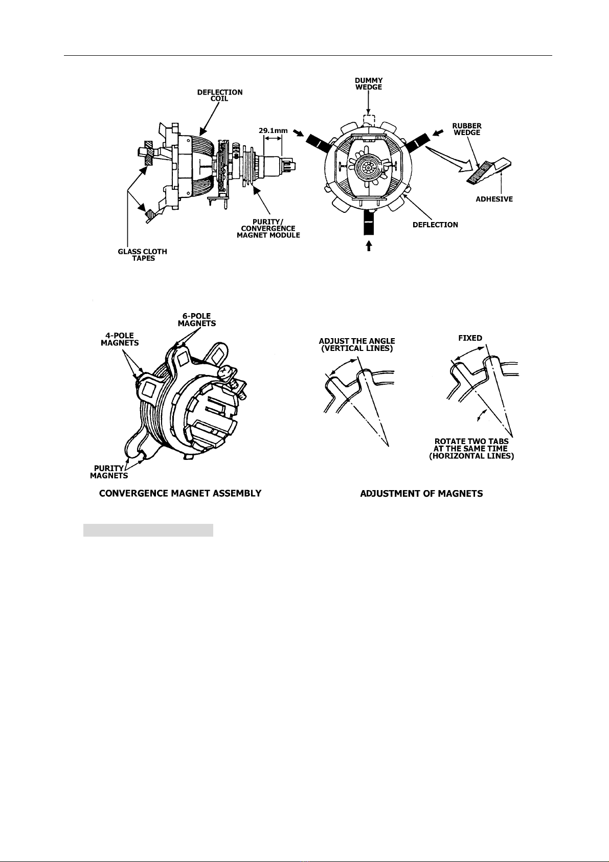
SERVICE MANUAL
Yoke
Fig. 1
Fig. 2
2. Convergence Adjustment
Preparation:
Before attempting any convergence adjustment, the TV should be operated for at least 15 minutes.
2.1 Center convergence adjustment
2.1.1 Receive dot pattern.
2.1.2 Adjust the brightness/contrast controls to obtain a sharp picture.
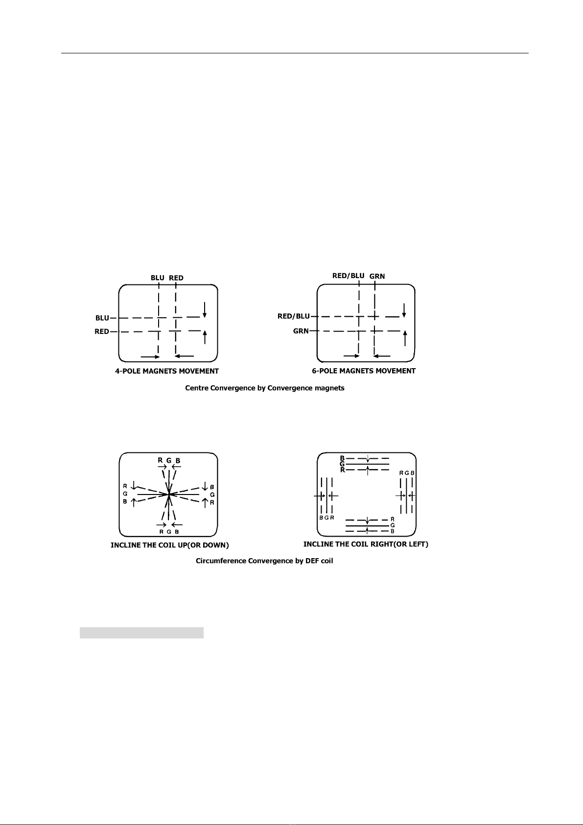
2.1.3 Adjust two tabs of the 4-pole magnet to change the angle between them and red and blue vertical
lines are superimposed each other on the center of the screen.
2.1.4 Turn both tabs at the same time keeping the angle constant to superimpose red and blue horizontal
on the center of the screen.
2.1.5 Adjust two tabs of the 6-pole magnet to superimpose red/blue line and green line.
2.1.6 Remember red and blue movement. Repeat steps 2.1.3~2.1.5 until optimal convergence is
obtained.
2.2 Circumference convergence adjustment
2.2.1 Loosen the clamp screw holding the deflection yoke assembly and allow it tilting.
6
Page 8
SERVICE MANUAL
2.2.2 Temporarily put the first wedge between the picture tube and deflection yoke assembly. Move front
of the deflection yoke up or down to obtain better convergence in circumference. Push the mounted
wedge in to fix the yoke temporarily.
2.2.3 Put the second wedge into bottom.
2.2.4 Move front of the deflection yoke to the left or right to obtain better convergence in circumference.
2.2.5 Fix the deflection yoke position and put the third wedge in either upper space. Fasten the deflection
yoke assembly on the picture tube.
2.2.6 Detach the temporarily mounted wedge and put it in either upper space. Fasten the deflection yoke
assembly on the picture tube.
2.2.7 After fastening the three wedges, recheck overall convergence and ensure to get optimal
convergence. Tighten the lamp screw holding the deflection yoke assembly.
4-pole Magnet Movement 6-pole Magnet Movement
Center Convergence by Convergence Magnets
Incline the Yoke Up (or Down) Incline the Yoke Right (or Left)
Circumference Convergence by DEF Yoke
Fig.3
3. White Balance Adjustment
Generally, white balance adjustment is made with professional equipment. It’s not practical to get good
white balance only through manual adjustment. For TVs with I
2
C bus control, change the bus data to
adjust white balance.
7
Page 9

SERVICE MANUAL
CIRCUIT ADJUSTMENTS
Preparation:
Circuit adjustments should be made only after completion of set-up adjustments.
Circuit adjustments can be performed using the adjustable components inside the TV set. For TVs with
2
I
C bus control, first change the bus data.
1. Degaussing
A degaussing coil is built inside he TV set. Each time the TV is powered on, the degaussing coil will
automatically degauss the TV. If the TV is magnetized by external strong magnetic field, causing color
spot on the screen, use a specific degausser to demagnetize the TV in the following ways. Otherwise,
color distortion will be exist on the screen.
1.1 Power on the TV set and operate it for at least 15 minutes.
1.2 Receive red full-field pattern.
1.3 Power on the specific degausser and face it to the TV screen.
1.4 Turn on the degausser. Slowly move it around the screen and slowly take it away from the TV.
1.5 Repeat the above steps until the TV is degaussed completely.
2. Supply Voltage Adjustment
Caution: +B voltage has close relation to high voltage. To prevent X-ray radiation, set +B voltage
to the rated voltage.
2.1 Make sure that the supply voltage is within the range of the rated value.
2.2 Connect a digital voltmeter to the +B voltage output terminal VD891 of the TV set. Power on the TV and
set the brightness and sub-brightness to minimum.
2.3 Regulate voltage adjustment components on the power PCB to make the voltmeter read 115±1V .
3. High V oltage Inspection
Caution: No high voltage adjustment components inside the chassis. Please perform high
voltage inspection in the following ways.
3.1 Connect a precise static high voltmeter to the second anode (inside the high voltage cap) of the picture
tube.
3.2 Plug in the supply socket (120V, AC) and turn on the TV. Set the brightness and contrast to minimum (0
μA).
3.3 The high voltage reading should be less than the EHT limitation.
3.4 Change the brightness from minimum to maximum, and ensure high voltage not beyond the limitation in
any case.
Nominal EHT voltage: 22±1KV Limited EHT voltage: 25KV
8
Page 10
SERVICE MANUAL
4. Focus Adjustment
Caution: Dangerously high voltages are present inside the TV. Extreme caution should be
exercised when working on the TV with the back removed.
4.1 After removing the back cover, look for the FBT on the main PCB. There should be a FCB on the FBT.
4.2 Power on the TV and preheat it for 15 min.
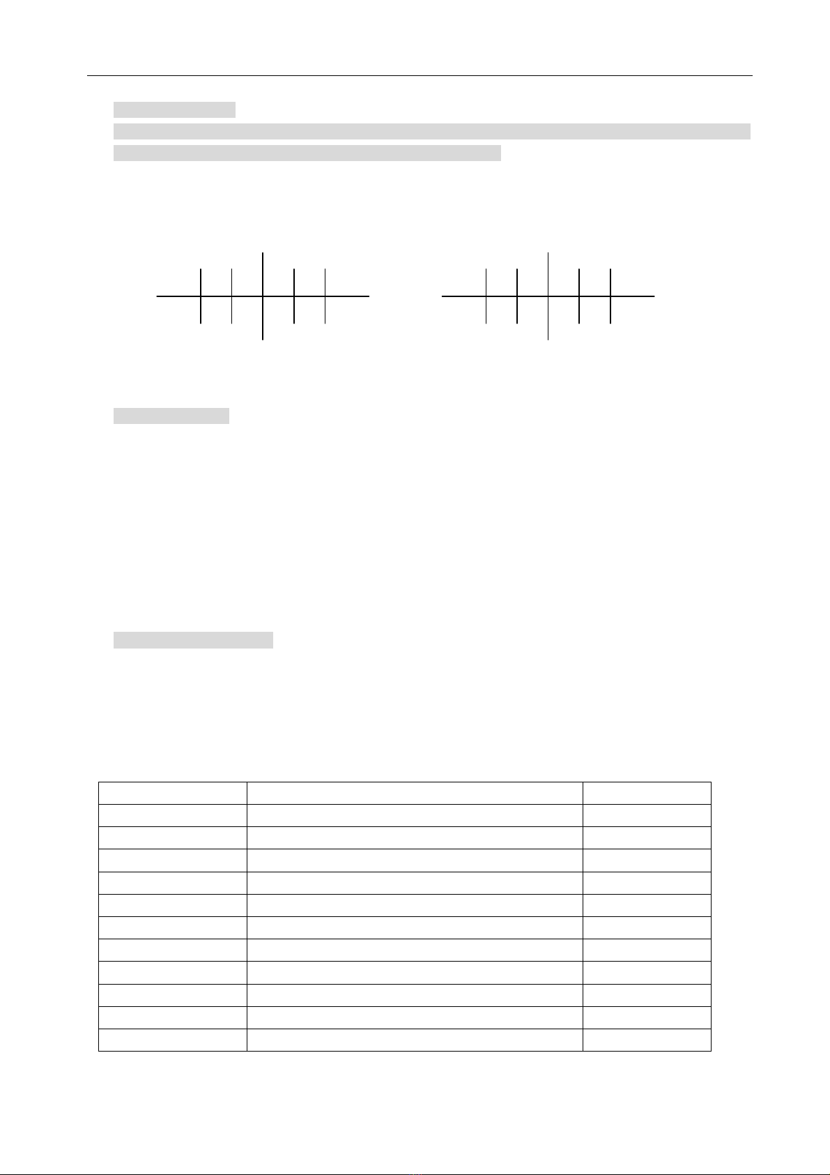
4.3 Receive a normal TV signal. Rotate knob of the FCB until you get a sharp picture.
Before Adjusting After Adjusting
5. Safety Inspection
5.1 Inspection for insulation and voltage-resistant
Perform safety test for all naked metal of the TV. Supply high voltage of 3000V AC, 50Hz (limit current of
10mA) between all naked metal and cold ground. Test every point for 3 seconds. and ensure no arcing
and sparking.
5.2 Requirements for insulation resistance
Measure resistance between naked metal of the TV and feed end of the power cord to be infinity with a
DC-500 high resistance meter and insulation resistance between the naked metal and degaussing coil
to be over 20MΩ.
6. DESIGN/SERVICE mode
6.1 To enter the DESIGN/USER SERVICE (S) mode
Set the volume to 0. Then press the MUTE key on the remote control and on the TV at the same time
for over 2 seconds. In the S mode, press the POWER key to quit the S mode.
6.2 Adjustments and bus data
Table 1 Bus Data
Item Symbol Description Bus Data
MENU.00
V.POSITION VERTICAL POSITION 40
H.PHASE HORIZONTAL PHASE 15
V.SIZE VERTICAL SIZE 60
V.SC VERTICAL S-CORRECTION 18
V.LINE VERTICAL LINE 19
V.SIZE CMP VERTICAL SIZE COMPENSATION 7
MENU.01
SUB.BIAS SUB-BRIGHT 63
SUB.CONT SUB-CONTRAST 31
V.KILL VERTICAL KILL 0
(continued)
9
Page 11

SERVICE MANUAL
RF.AGC RF AGC 20
R.BIAS RED BIAS 130
G.BIAS GREEN BIAS 130
B.BIAS BLUE BIAS 130
R.DRIVE RED DRIVE 75
G.DRIVE GREEN DRIVE 15
B.DRIVE BLUE DRIVE 75
MENU.02
SECAM B DC SECAM B-Y 0
SECAM R DC SECAM R-Y 0
H.APC GAIN HORIZONTAL APC GAIN 0
SYNC.KIL SYNC KILL 0
H.BLK.L HORIZONTAL BLANKING LEFT 4
H.BLK.R HORIZONTAL BLANKING RIGHT 4
CROS.B/W CROSSHATCH BLACK/WHITE 0
VIDEO.LVL VIDEO LEVEL 7
FM.LEVEL FM LEVEL 16
MENU.03
FM.MUTE FM MUTE 0
AUDIO.MUTE AUDIO MUIE 0
VIDEO.MUTE VIDEO MUTE 0
DEEM.TC DE-EMPHASIS TIME CONSTANT 0
SND.TRAP SOUND TRAP 0
MENU.04
SUB.COLOR SUB COLOR 63
SUB.TINT SUB TINT 32
SUB.SHARP SUB SHARP 63
AUTO FLESH AUTOMATIC FLESH 0
CORING.GAN CORING GAIN 1
C.EXT EXTERNAL CHROMA 0
C.BYPASS CHROMA BAND-PASS BYPASS 0
C.KILL ON COLOR KILL ON 0
MENU.05
FIL.SYS
FILTER SYSTEM:SELECT Y/C FILTER MODE
1
COLOR.SYS COLOR SYSTEM 5
VOL.FIL VOLUME FILTER 0
VIF.SYS VIF SYSTEM 0
SIF.SYS.SW SIF SYSTEM SWITCH 0
VIDEO.SW VIDEO SWITCH 1
MENU.06
R/B G.BAL R-Y/B-Y GAIN BALANCE 7
R/B ANGLE R-Y/B-Y ANGLE 9
CD MODE VERTICAL COUNTDOWN MODE 0
(continued)
10
Page 12

SERVICE MANUAL
GREY MODE GREY MODE 0
V.SETUP VERTICAL SETUP 1
MENU.07
BLANK.DEF BLANK DEFEAT 0
BRT.ABL.TH BRIGHT ABL THRESHOLD 7
RGB TEMP RGB TEMPERATURE SWITCH 1
BRT.ABL.DF BRIGHT ABL DEFEAT 0
MID.STP.DF BRIGHT MID STOP DEFEAT 0
FBP.BLK.SW
FLYBACK PULSES (HORIZONTAL)BLANKING
0
SWITCH
MENU.08
DIGITAL.OSD DIGITAL OSD MODE 0
OSD.CONT OSD CONTRAST CONTROL 10
OSD.CONTST OSD CONTRAST TEST 0
OSD.H.POS OSD HORIZONTAL POSITION 22
MENU.09
H.FREQ HORIZONTAL FREQUENCY 46
FM.GAIN FM GAIN 0
C.KILL.OFF COLOR KILL OFF 0
AUDIO.SW AUDIO SWITCH 0
T.DISBLE TEST MODE SWITCH DISABLE 1
MENU.10
G/Y ANGLE G/Y ANGLE 0
COL KIL OP COLOR KILLER OPERATIONAL LEVEL 5
CBCR-IN YCBCR INPUT 1
Y-APF
YC
MODE,ALL PASS FILTER MODE
BCR
0
PRE SHOOT PRE-SHOOT WIDTH 0
WPL OPE WHITE PEAK LIMITER LEVEL OPERATE 0
DC REST LUMA DC RESTORATION 0
BK STR STA BLACK STRETCH START POINT 1
BK STR GAN BLACK STRETCH START GAIN 1
MENU.11
OVER MD SW 1
Y GAMMA Y GAMMA START POINT 0
FSC C.SYNC fSC C-SYNC OUTPUT 1
VBLK SW VERTICAL BLANKING CONTROL SWITCH 0
SND TRAP SOUND TRAP 1
HALF TONE HALF TONE LEVEL 3
HALF T SW HALF TONE ON/OFF SWITCH 1
TST VERSET 0
MENU.12
E/W DC
E/W(EAST/WEST)
32
E/W AMP E/W 32
(continued)
11
Page 13

SERVICE MANUAL
E/W TILT E/W 32
E/W C TOP E/W 5
E/W C BOTM E/W 5
MENU.13
E/W TEST E/W TEST 7
HSIZE COMP HORIZONTAL SIZE COMPENSATION 7
IF TEST 3B 3dB IF TEST 0
V.LEV ADJ VIDEO LEVEL ADJUSTMENT 0
OV MOD LEV 5
PRE/OVER PRE/OVER-SHOOT ADJUSTMENT 0
C.VCO SW CHROMA VCO(VOLTAGE CONTROLLED OSCILLATOR)SWITCH 0
C.VCO ADJ CHROMA VCO ADJUSTMENT 0
MENU.14
VNSYNC 0
TINT.THROU TINT THROUGH 0
HLOCK.VDET 0
MENU.15
OPT.1CHIP OPTION 1CHIP 1
OPT.VIDEO OPTION VIDEO 1
OPT.DVD OPTION DVD 1
OPT.AV1AV2 OPTION AV1/AV2 1
OPT.AV3 OPTION AV3 0
OPT.S-VHS OPTION S-VHS 1
OPT.YUV OPTION YUV 0
OPT.COMB OPTION COMB 0
OPT.BYPASS OPTION BYPASS 0
MENU.16
OPT . VM OPTION VM 0
OPT.BLUEBK OPTION BLUEBK 1
OPT.V-CHIP OPTION V-CHIP 1
OPT.CCD OPTION CCD 1
OPT.CLOCK OPTION CLOCK 1
OPT.P-ON OPTION 0
SRCH.SPEED SEARCH SPEED 0
ROM .CORREC ROM CORRECTION 0
MENU.17
OPT.BTSC OPTION BTSC 1
OPT.AV-INP OPTION AV-INP 0
OPT.BBE OPTION BBE 0
OPT. DVD-IN
SUB.BASS SUB BASS 3
SUB.TREBLE SUB TREBLE 3
OPTION DVD-IN 0
(continued)
12
Page 14

SERVICE MANUAL
MENU.18
LOUNDNESS LOUDNESS 9
FM/AM.PRES FM/AM PRESETTING 63
SCART.PRES SCART PRESETTING SCART VOLUME 39
SCART.VOL SCART VOLUME 117
OPT.AVC OPTION AVC 1
AVC.DECAY 2
BBE.BASS BBE BASS 32
BBE.TREBLE BBE TREBLE 32
Notes:
① The data sheet may differ dependent on different models.
② The data sheet may differ dependent on different CRTs for the same model.
13
Page 15

SERVICE MANUAL
ADJUSTMENTS FOR DVD UNIT
1. Power on the unit only after ensuring DVD130A modules is connected correctly in accordance with the
wiring diagram.
2. If the unit fails to play after power-on, repair the DVD130A according to the service illustration until it can
read discs and has corresponding AV output.
3. Inspect audio output of the DVD130A in the following ways.
a. Inspect digital audio output: When playing a disc, connect a signal cable to the coaxial output
terminal. Press the SETUP button on the remote control and set “AUDIO OUT” in the SETUP
menu to “SPDIF/SOURCE CODE”. Then start playback with the PLAY button and the following
diagram will be displayed with waveform amplitude of 0.75±0.25Vpp on the oscilloscope. After
inspection, set “AUDIO OUT”to “ANALOG”.
b. Connect the OUT terminal on the DVD130A to the IN terminal on the TV and shift the TV to the DVD
mode. After power-on for several seconds, the TV should display the preset LOGO picture on the
screen, which should be smooth and distort-free with normal color. Press the OPEN/CLOSE button
on the remote control to open the disc tray. Place the disc on the disc tray. Press the PLAY button
and play should begin after several seconds. The color and sound should be normal, and picture
should be smooth and distortionless.
c. With a CD disc played, the TV should display the preset LOGO picture on the screen. The color
and sound should be normal, and picture should be smooth and distortionless.
14
Page 16
SERVICE MANUAL
STRUCTURE AND CHASSIS FUNCTION DESCRIPTION
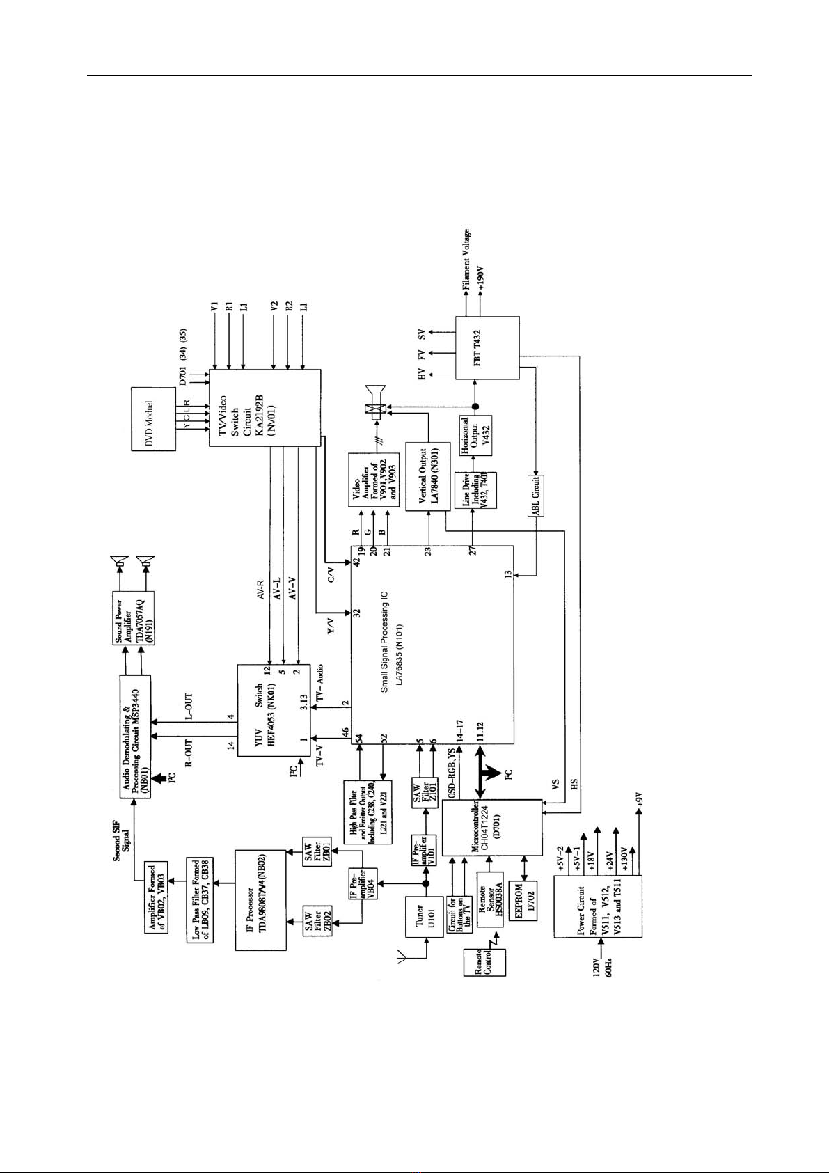
1. STRUCTURE BLOCK DIAGRAM (For CPU CH04T1224 Only)
15
Fig. 4 Structure Block Diagram for CN-12DV Chassis
Page 17
SERVICE MANUAL
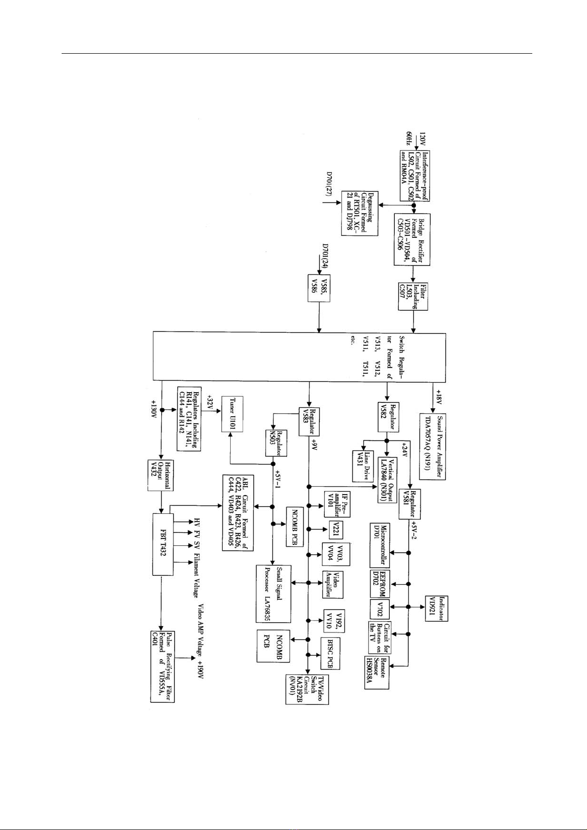
3.BLOCK DIAGRAM OF SUPPLY VOLTAGE SYSTEM
Fig. 6 Block Diagram for CN-12DV Supply Voltage System
16
Page 18
SERVICE MANUAL
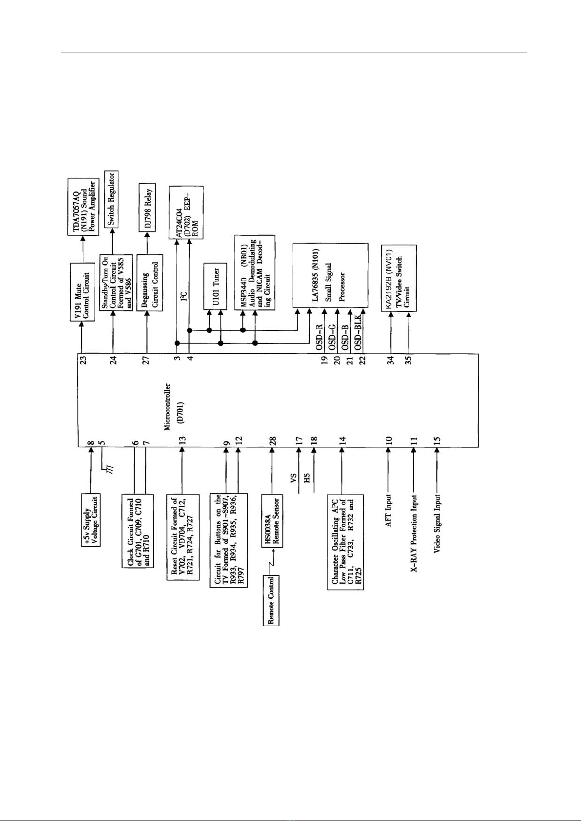
4. BLOCK DIAGRAM OF REMOTE CONTROL SYSTEM
Fig. 7 Block Diagram for CN-12DV Remote Control Structure
17
Page 19
SERVICE MANUAL
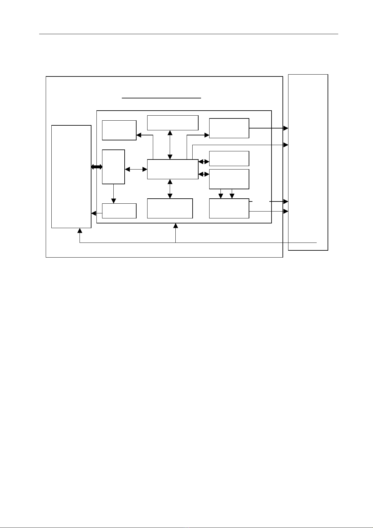
4.STRUCTURE BLOCK DIAGRAM FOR DVD130A
DVD130A MODULE
EEPROM
24C01
2X16M SDRAM
CS4955-CD
Sanyo
MT1336E
+DJ-100
Pickup head
BA5954
MT1369AE
8M FLASH
L
74HCU04
CS4340
Audio DAC
R
NJM4558M
Audio Amp
S-VIDEO
SPDIF
L-out
R-out
TV
Power Supply
Fig.
8 Structure Block Diagram for DVD130A
18
Page 20
SERVICE MANUAL
5.CHASSIS FUNCTION DESCRIPTION
5.1. General Description
MTV-DV05 TV/DVD combo has combined function of TV signal reception and DVD discs playback, of
which TV unit uses CN-12C2 chassis and DVD unit uses loader DVD 130A.
CN-12C2 chassis applies a single chip IC LA76835 of Japan-based Sanyo for small signal processing,
featuring multi system reception. The applied I
control the TV for much convenience of operation and servicing. Refer to Fig.4 about the chassis’
structure block diagram.
Compatible with DVD, CD, VCD, SVCD, MP3, and KODAR Picture CD, DVD130A, high-quality modules
with various functions, features multi angle, multilingual and multi captions. With Dolby dual channel
amplifying and DTS coaxial cable, the DVD audio system offers astonishingly high-quality audio output.
DVD130A consists of a disc tray (including DJ-100 assembly and small loader DV-33FS) and analog
signal processor/servo control/MPEG decoding board MT1369AE+MT1336E. The servo control/MPEG
decoding board MT1369AE, developed by MEDIATEK, is designed for use in signal control, decoding,
data processing, etc., featuring servo control, AV decoding, analog front end, DPU (DATA PATH UNIT),
2
C bus control technology can automatically adjust and
main axis control, CSS/CPPM module, system analysis program, video output unit, audio terminals and
system control. MT1336E, also
developed by MEDIATEK, is a high-performance CMOS analog signal processor with servo amplifying
and DPD tracking error signal for use in CD-ROM drive and DVD-RAM. For DVD-RAM, MT1336E also
uses DPP for developing tracking signal and DAD for processing focus signal. Meanwhile, the IC,
programmable, is equipped with a separate DVD-ROM, CD-ROM two-way automatic laser power
control circuit and reference voltage generator.
5.2 Key ICs and Assemblies
5.2.1 The CN-12C2 chassis mainly uses the following ICs and assemblies.
Table 2 Key ICs and Assemblies of CN-12C2 Chassis
Serial No. Position Type Function Description
1 D701
2 D702 AT24C08
3 N101 LA76835
4 NV01 KA2192B
5 N301 LA7840
6 N191 TDA7057AQ
CH04T1227
Microcontroller
EEPROM
Small signal processor
TV/Video switch circuit
Vertical output circuit
Sound power amplifier
7 NN01 TDA9808T Audio IF demodulator
8 NN02 MSP3410G NICAM audio processor
9 N503 LM7805
10 NK01 HEF4053
11 U101 TDQ-3B8/136
Tri-pin regulator
Electronic switch circuit
Tuner
19
Page 21
SERVICE MANUAL
5.2.2. The DVD130A mainly uses the following ICs and assemblies.
Table 3 Key ICs and Assemblies of DVD130A
Serial No. Position Type Function Description
MPEG board Drawing No. JUV2.033.071-1MX
1 U1 MT1336E RF amplifier
2 U2 BA5954FM Focus/tracking coil and feed motor drive
3 U3 MT1369AE MPEG decoder
4 U5 74HCU04 Enhancement drive
5 U7 8M FLASH Flash memory
6 U9 NJM4558M Sound amplifier
7 U10 24C01 1K EEPOM
8 U13 CS4340 Audio D/A controller
9 U14 CS4955-CD Video encoder
10 U17 16M SDRAM Dynamic EEPROM
DJ-100 Disc tray assembly
20
Page 22

SERVICE MANUAL
SERVICE DATA
SERVICE DATA FOR TV UNIT
TECHNICAL DATA OF KEY ICS
CH04T1227 (D701)
8-Bit Single Chip Microcontroller
1. Overview
The LC86F344BA are 8-bit single chip microcontrollers with the following on-chip functional blocks:
-CPU:Operable at a minimum bus cycle time of 0.424µs
-On-chip ROM capacity
Program ROM:32K/28K/24K/20K/16K bytes
CGROM:16K bytes
-On-chip ROM capacity: 512 bytes
-OSD RAM: 352×9 bits
-Closed-Caption TV controller and the on-screen display controller
-Closed-Caption data slicer
-Four channels×6-bit AD Converter
-Three channels×7-bit PWM
-16-bit timer/counter,14-bit base timer
-IIC-bus compliant serial interface circuit (Multi-master type)
-ROM correction function
-11-source 8-vectored interrupt system
-Integrated system clock generator and display clock generator
Only one X’tal oscillator (32.768kHz) for PLL reference is used for both generators
TV control and the Closed Caption function
All of the above functions are fabricated on a single chip.
21
Page 23
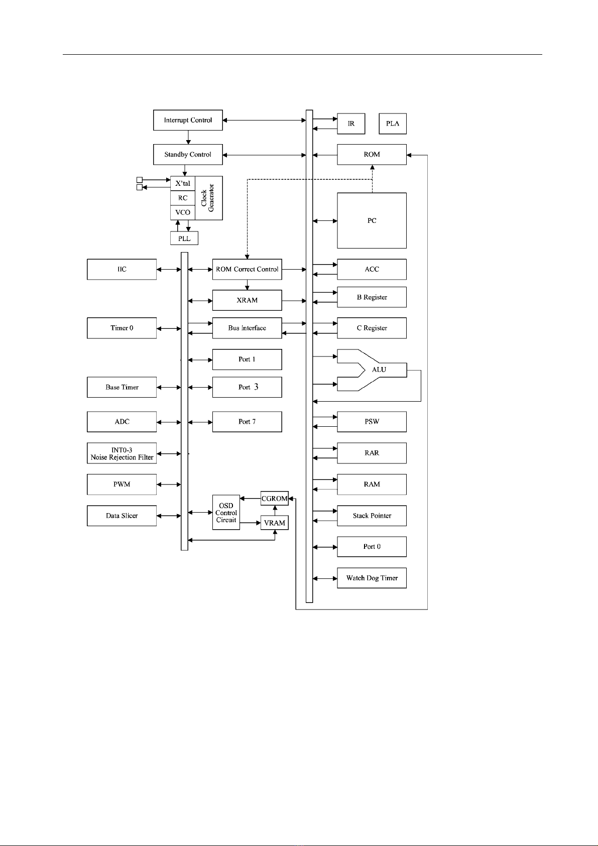
2. System Block Diagram
SERVICE MANUAL
Fig. 9
3. Refer to Table 4 about Functions and Service Data of the IC’s Pins.
22
Page 24
SERVICE MANUAL
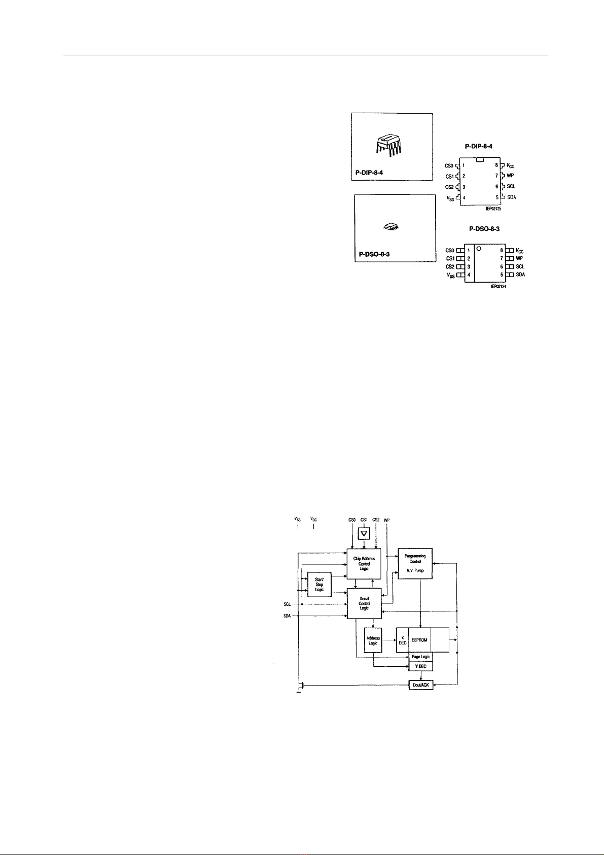
AT24C08 (D702)
EEPROM
1. Features
·Data EEPROM internally organized as 1024/2048 bytes
and 64/128 pages×16 bytes
·Page protection mode, flexible page-by-page hardware
write protection
- Additional protection EEPROM of 64/128 bits, 1 bit per
data page
- Protection setting for each data page by writing its
protection bit
- Protection management without switching WP pin
·Low power CMOS
·Vcc=2.7 to 5.5V operation
·Two wire serial interface bus, I
·Filtered inputs for noise suppression with Schmitt trigger
·Clock frequency up to 400 kHz
·High programming flexibility
- Internal programming voltage
- Self timed programming cycle including erase
- Byte-write and page-write programming, between 1 and 16 bytes
- Typical programming time 6 ms(<10ms) for up to 16 bytes
·High reliability
- Endurance 10
- Data retention 40 years
6
cycles1)
1)
- ESD protection 4000 V on all pins
·8 pin DIP/DSO packages
·Available for extended temperature ranges
- Industrial: -40℃ to +85℃
- Automotive: -40℃ to +125℃
3. Block Diagram
2
C-Bus compatible
2. Pin Configuration
Fig.10
4. Refer to Table 5 about Functions and Service Data of AT24C08’s Pins.
23
Page 25

SERVICE MANUAL
KA2192B (NV01)
TV/Video Switch Circuit
1. Features
The TV/Video switch circuit KA2192B (NY01) is an electronic switch circuit controlling four sets of audio
signal inputs, three sets of video signal inputs, two sets of Y/C separation signals inputs, one set of video
signal output, one set of Y/C separation signal output and one set of audio signal output.
2. Block Diagram
Fig.11
3. Value Table
Level for Control Terminal
(15) (16)
H H TV
H L AV1
L H SVHS
L L AV2
4. Refer to Table 6 about Functions and Service Data of KA2192B’s Pins.
Switchover Mode
24
Page 26
SERVICE MANUAL
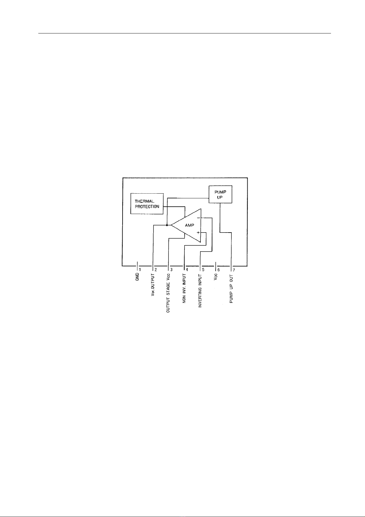
LA7840 (N301)
Vertical Deflection Output Circuit
1. Features
·Low power dissipation due to built-in pump-up circuit
·Vertical output circuit
·Thermal protection circuit built in
·Excellent crossover characteristics
·DC coupling possible
2. Block Diagram
Fig. 12
3. Refer to Table 7 about Functions and Service Data of LA7840’s Pins.
25
Page 27
SERVICE MANUAL
TDA7057AQ (N191)
2×8W Stereo BTL Audio Output Amplifier with DC Volume Control
1. Features
·DC volume control
·Few external components
·Mute mode
·Thermal protection
·Short-circuit proof
·No switch-on and switch-off clicks
·Good overall stability
·Low power consumption
·Low HF radiation
·ESD protected on all pins.
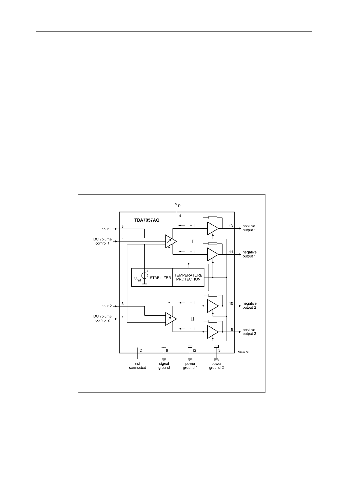
3. Block Diagram
Fig.13 Block Diagram
4. Refer to Table 8 about Functions and Service Data of TDA7057AQ’ s Pins.
26
2. General Description
The TDA7057AQ is a stereo BTL output amplifier
with DC volume control. The device is designed
for use in TVs and monitiors, but is also suitable
for battery-fed portable recorders and radios.
Missing Current Limiter (MCL)
A MCL protection circuit is built-in. The MCL
circuit is activated when the difference in current
between the output terminal of each amplifier
exceeds 100mA (typical 300 Ma). This level of
100mA allows for single-ended headphone
applications.
Page 28
SERVICE MANUAL
HEF4053 (NK01)
Triple 2-channel Analog Multiplexer/Demultiplexer
1. Description
The HEF4053 is a triple 2-channel analog
multiplexer/demultiplexer with a common enable
input (E). Each multiplexer/ demultiplexer has two
independent inputs/ outputs (Y
common input/ output (Z), and select inputs (Sn).
Each also contains two-bidirectional analog
switches, each with one side connected to an
independent input/output (Y
other side connected to a common
input/output(Z).
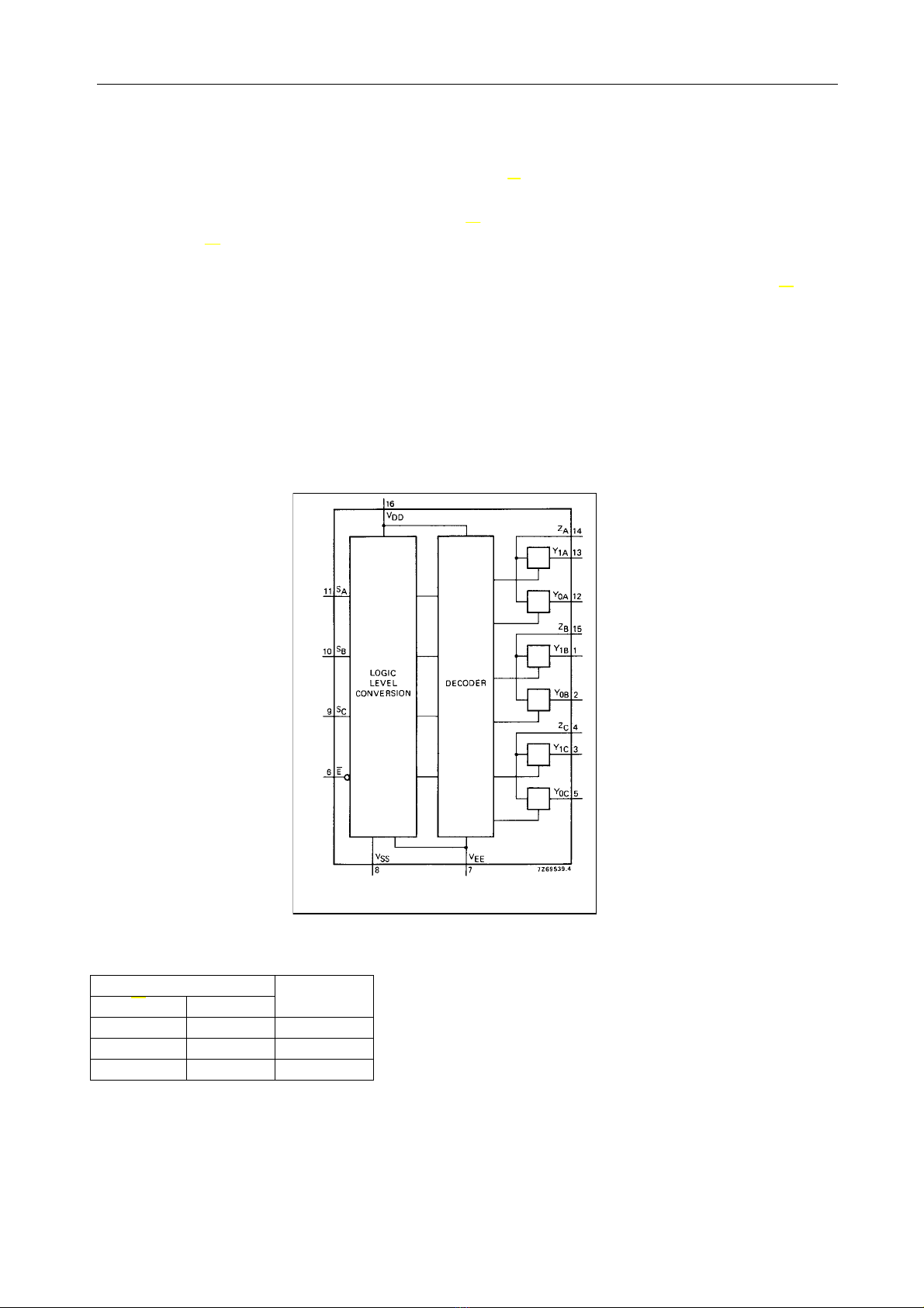
2. Block Diagram
and Y1), a
0
and Y1) and the
0
With (E) LOW, one of the two switches is selected
(low impedance ON-state) by Sn. With E HIGH, all
switches are in the high impedance OFF-state,
independent of S
V
and VSS are the supply voltage connections
DD
to SC.
A
for the digital control inputs (SA to SC and E).
The V
to VSS range is 3 to 15V.The analog
DD
inputs/outputs (Y0,Y1 and Z) can swing between
V
as a positive limit and VEE as a negative limit.
DD
V
may not exceed 15 V.
DD-VEE
For operation as a digital multiplexer/
demultiplexer, V
is connected to VSS (typically
EE
ground).
3. Function Table
Inputs
E Sn
Channel
On
L L Yon-Zn
L H Yin-Zn
H X none
Fig. 14 Functional Diagram
Notes
H=HIGH state (the more positive voltage)
L=LOW state (the less positive voltage)
X=STATE is immaterial
4. Refer to Table 11 about Functions and Data of HEF4053’s Pins.
27
Page 29

SERVICE MANUAL
TDA9808T
SINGLE STANDARD VIF-PLL WITH QSS-IF AND FM-PLL DEMODULATOR
1. Features
·5V supply voltage (9V supply voltage for
TDA9808T (DIP20) only)
·Applicable for IFs (lntermediate Frequencies) of
38.9MHz, 45.75MHz and 58.75 MHz
·Gain controlled wide band Video IF (VIF)amplifier (AC-coupled)
·True synchronous demodulation with active carrier
regeneration (very linear demodulation, good
intermodulation figures, reduced harmonics,
excellent pulse response)
·Robustness for over-modulation better than 105%
due to Phase Locked Loop (PLL)-bandwidth control
at negative modulated standards
·VIF Automatic Gain Control (AGC) detector for gain
control, operating as peak sync detector
·Tuner AGC with adjustable TakeOver Point (TOP)
·Automatic Frequency Control (AFC) detector
without extra reference circuit
·AC-coupled limiter amplifier for sound intercarrier
signal
·Alignment-free FM-PLL demodulator with high
linearity
·Sound IF (SIF) input for single reference Quasi
Split
Sound (QSS) mode (PLL controlled); SIF AGC
detector for gain controlled SIF amplifier, single
reference QSS mixer for high performance
·Electrostatic Discharge (ESD) protection for all
pins.
2. General Description
The TDA9808T is an integrated circuit for
single standard (negative modulated) vision
IF signal processing and FM demodulation,
with single reference QSS-IF in TV and VTR
sets.
28
Page 30
SERVICE MANUAL
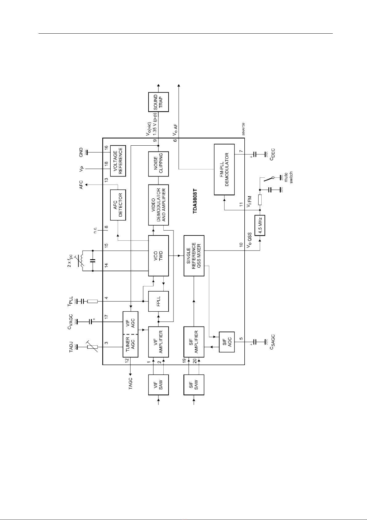
3. Block Diagram
4. Refer to Table 20 about Functions and Data of the IC’s Pins.
Fig. 15 Block Diagram
29
Page 31
SERVICE MANUAL
MSP34X0G
MULTISTANDARD SOUND PROCESSOR FAMILY
Release Note: Revision bars indicate significant
changes to the previous edition. The hardware
and software description in this document is
valid for the MSP34X0G version B5 and following
versions.
1. Introduction
The MSP34X0G family of single-chip
Multistandard Sound Processors covers
the sound processing of all analog
TV-Standards worldwide, as well as the
NICAM digital sound standards. The full TV
sound processing, starting with analog sound IF
signal-in, down to processed analog AF-out, is
performed on a single chip. Figure 10 shows a
simplified functional block diagram of the
MSP34X0G.
This new generation of TV sound processing ICs
now includes versions for processing the
multichannel television sound (MTS) signal
conforming to the standard recommended by the
Broadcast Television Systems Committee
(BTSC). The DBX noise reduction, or
alternatively MICRONAS Noise Reduction
(MNR) is performed alignment free.
Other processed standards are the Japanese
FM-FM multiplex standard (EIA-J) and the
FM Stereo Radio standard.
Current ICs have to perform adjustment
procedures in order to achieve good stereo
separation for BTSC and EIA-J.
The MSP34X0G has optimum stereo
performance without any adjustments.
All MSP34X0G versions are pin and
software downward-compatible to the
MSP34X0G. The MSP34X0G further simplifies
controlling software. Standard selection
requires a single I
The MSP34X0G has built-in automatic
Functions: The IC is able to detect the actual
sound standard automatically (Automatic
Standard Detection). Furthermore, pilot levels
and identification signals can be evaluated
internally with subsequent switching between
mono/stereo/bilingual, no I
necessary (Automatic Sound Selection).
The ICs are produced in submicron CMOS
technology.
The MSP34X0G is available in the following
packages, PLCC68, PSDIP64, PSDIP52,
PQFP80 and PLQFP64.
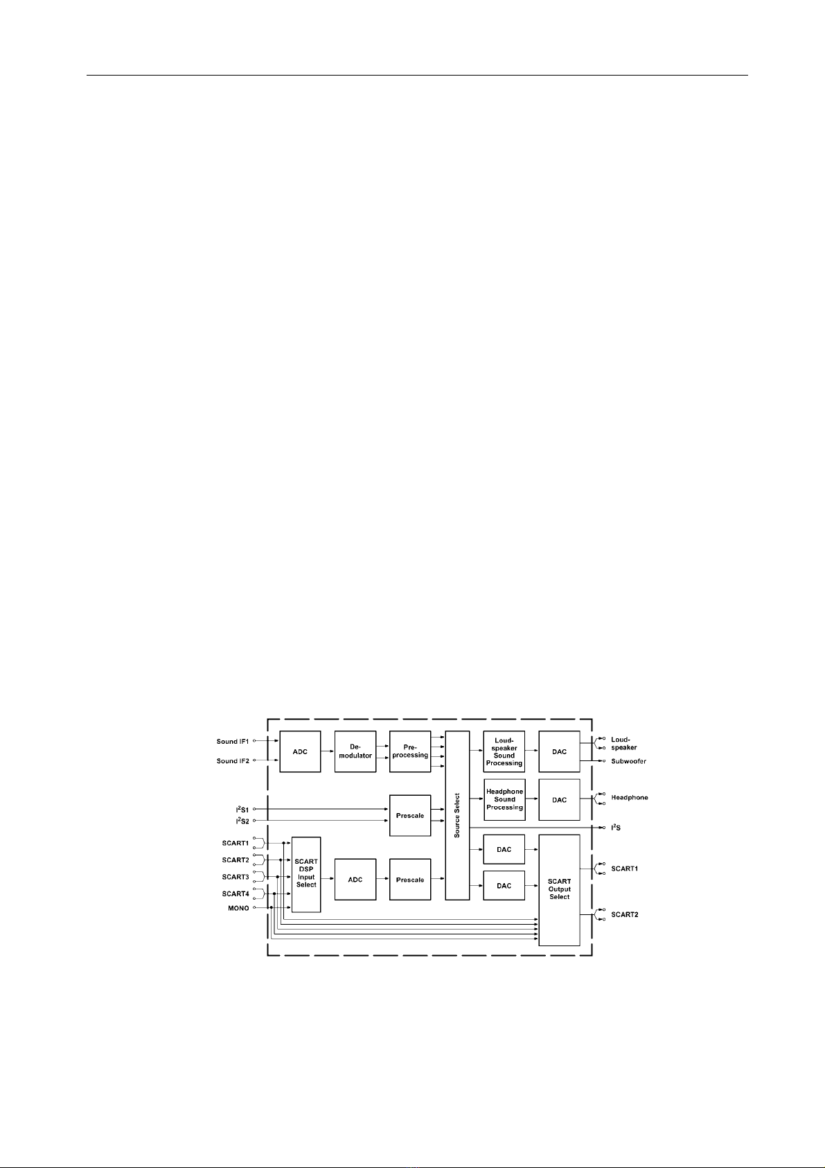
2. Block Diagram
Fig. 16 Simplified Functional Block Diagram of the MSP34X0G
3. Refer to Table 21 about Functions and Data of the IC’s Pins.
2
C transmission only.
2
C interaction is
30
Page 32
SERVICE MANUAL
SERVICE DATA OF KEY ICS
Table 4 Functions and Service Data of LA76835 (N101)’s Pins
GDM8145 Multimeter
Ground Resistance (Ω)
Pin
No.
Function Description
Voltage
of
Pin (V)
Measure with
red probe
while
grounding
black probe.
1 Audio signal output (NC) 2.33 810 712
2 Audio demodulation output 2.36 975 675
3 IF AGC filter 2.6 860 718
4 RFAGC voltage output 1.95 ∞ 680
5 IF signal input 2.89 780 693
6 IF signal input 2.89 778 712
7 IF circuit ground 0 0 0
8 Supply voltage for IF circuit 5.04 500 280
9 Filter for discriminator 1.98 910 713
10 AFT voltage output 3.65 910 617
11 I2C bus data line 4.71 1560 640
12 I2C bus clock line 4.41 1542 667
13 Auto brightness control input 3.68 945 577
14 R character signal input 1.43/0 920 700
15 G character signal input 1.46/0 913 701
16 B character signal input 1.44/0 906 700
17 Supply voltage for decoder 0.02/0 780 683
18 Red (R) signal output 8.28 525 500
19 Green (G) signal output 2.81 780 671
20 Blue (B) signal output 2.79 780 670
21 Character blanking signal input 2.7 780 670
22 White balance adjusting signal input (NC) 1.85 830 696
23 Vertical sawtooth output 2.45 710 672
24 Vertical sawtooth generation 2.64 782 702
25 Horizontal start supply voltage 5.27 350 350
26 Low pass filter for horizontal AFC 2.72 815 708
27 Line drive pulse output 0.72 700 653
28 Line flyback pulse input 0.91 785 707
29 Reference voltage generation terminal 1.74 746 700
30 B-Y color difference signal input (SECOM) 0.93 825 608
31 C-Y color difference signal input (SECOM) 0.94 330 330
32 External video/chroma signals inputs 4.17 ∞ 567
33 1H baseband delay circuit ground 0 0 0
Measure with
black probe
while
grounding
red probe.
31
(continued)
Page 33
34
X-RAY detection input
SERVICE MANUAL
0 775 712
35
36
37
38
39
40
41
42
43
44
45
46
4.43MHz CW signal output or SECAM killer
signal input
AFC filter for color sub-carrier
Clamp filter
4.43 MHz crystal oscillator connection
APC filter
Video signal output (NC)
Video/chroma/scan part ground
Video signals input from AV terminals or Y
signal input from S-VIDEO terminal
Supply voltage for video/chroma/scan part
C signal input from AV terminals or S-VIDEO
terminal (NC)
Filter for black level stretch
Video detection output
2.05 776 712
3.41 810 724
0 800 706
2.83 790 716
1.89 760 697
2.76 730 662
0 0 0
2.93 800 711
4.99 285 280
2.76 805 707
3.16 762 700
2.9 397 397
47
48
49
50
51
52
53
54
IF lock detection filter
External VCO harmonic oscillating coil
External VCO harmonic oscillating coil
IF PLL APC filter
Audio signal input (NC)
Sound IF output
APC filter for audio discrimination
Sound IF input
3.58 840 712
4.29 526 526
4.29 530 530
2.47 820 698
2.23 800 701
1.94 809 697
2.41 808 691
3.17 824 712
Table 5 Functions and Service Data of CH04T1227 (D701)’s Pins
GDM8145 Multimeter
Ground Resistance (KΩ)
Pin
No.
1
Function Description
Not connected
Voltage
of
Pin (V)
Measure with
red probe
while
grounding
black probe.
1.50 11.8 4.40
Measure with
black probe
while
grounding
red probe.
2
Not connected
32
1.43 12.1 5.20
(continued)
Page 34
SERVICE MANUAL
3
4
5
6
7
8
9
10
11
12
13
14
15
16
Bus data line
Bus clock line
Ground
Input terminal for clock oscillating signal
Output terminal for clock oscillating signal
Supply voltage
Button-control voltage input terminal 1
AFT voltage input terminal
X-RAY detection input
Button-control voltage input terminal 2
Reset
Character oscillating filter
Video signal input terminal
Three bits input/output terminals
4.70 11.6 6.20
4.47 12.1 6.00
0.00 0.00 0.00
1.78 12.6 5.1
2.88 12.0 4.91
5.31 7.90 3.72
0.02 9.70 5.34
2.47 4.90 5.08
2325 6.70 4.59
0.015 8.86 3.81
5.27 4.67 1.88
3.87 1.11 4.98
3.53 12.3 4.50
0.01 9.76 15.0
17
18
19
20
21
22
23
24
25
26
27
28
29
30
31
32
33
34
35
36
Input terminal for vertical flyback pulse
Input terminal for horizontal flyback pulse
R character output terminal
G character output terminal
B character output terminal
Output terminal for fast blanking signal
Mute
Standby control
Not connected
Control terminal for production modes
Degaussing circuit control
Remote control signal input
Not connected
Not connected
Not connected
Not connected
Output terminal for on/off control signals
Output terminal for AV2 on/off control
Output terminal for AV1 on/off control
Output terminal for AV0 on/off control
5.07 15.4 18.1
4.62 17.4 18.4
0.015 3.92 3.29
0.014 3.95 3.71
0.015 3.19 3.66
0.015 6.50 3.67
0.015 18.7 17.62
0.015 1.43 7.30
1.23 9.50 6.65
4.61 13.0 6.95
0.014 3.713 3.42
5.19 12.2 5.32
5.30 12.4 5.49
5.30 12.6 5.42
0.01 12.7 5.35
0.01 12.7 5.30
5.30 12.7 6.59
5.30 11.8 6.36
5.30 11.4 6.33
5.29 11.2 6.33
33
Page 35
Table 6 Functions and Service Data of AT24C08 (D702)’s Pins
Pin No. Function Description
SERVICE MANUAL
Voltage of
Pin (V)
GDM8145 Multimeter
Ground Resistance (KΩ)
Measure with red
probe while
grounding black
probe.
Measure with
black probe while
grounding red
probe.
1
2
3
4
5
6
7
8
Pin
No.
Address terminal 0
Address terminal 1
Address terminal 2
Ground
Data line
Clock line
Write-in/read-out control terminal
Supply voltage
Table 7 Functions and Service Data of KA2192B (NV01)’s Pins
Function Description
0 0 0
0 0 0
0 0 0
0 0 0
4.8 11.7 5.25
4.8 11.72 5.5
0 0 0
5 6.7 4
DT890D Digital Multimeter
Ground Resistance (KΩ)
Voltage
of
Pin (V)
Measure with
red probe
while
grounding
black probe.
Measure with
black probe
while
grounding
red probe.
1
L TV IN
2
R TV IN
3
TV IN
4
LS IN
5
RS IN
6
SY IN
7
TV SW
8
SC IN
9
L1 IN
10
11
12
34
R1 IN
E1 IN
L2 IN
5.67 6.45 3.53
5.67 6.45 3.74
5.67 6.57 4.02
5.69 6.45 3.66
5.69 6.47 3.72
5.54 6.85 3.96
0.00 0.00 0.00
5.54 6.75 3.85
5.69 6.43 3.36
5.70 6.37 3.72
5.56 6.85 3.96
5.70 6.43 3.87
(continued)
Page 36
SERVICE MANUAL
13
14
15
16 5.25 6.85 5.59
17
18 3.89 1.418 1.51
19
20
21
22
23 0.06 3.97
24
25 3.47 6.80 5.75
26
R2 IN
E2 IN
SW1
SW2
MUTE
Y OUT
GND
C OUT
R OUT
L OUT
NC
Y IN
SYNC CLAMP
C IN
5.70 6.33
5.56 4.01
5.25
6.83
6.84 5.59
3.67
0.00 0.00 0.00
0.00 0.00 0.00
3.84 0.96
4.37 3.35
4.37
0.63
6.61 3.31
1.15
6.71
5.55
6.70 4.18
5.57 6.67 4.07
27
28
29
30
Pin
No.
1
2
3
4
NC
VCC
VCC
VOUT
Table 8 Functions and Service Data of LA7840 (N301)’s Pins
Function Description
Ground
Vertical output terminal
Pump supply voltage input
Reference voltage
0.25 6.69 4.13
9.38 0.34 0.33
9.38 0.31 0.30
3.17 6.47 0.48
DT890D Digital Multimeter
Ground Resistance (Ω)
Voltage of
Pin (V)
Measure with red
probe while
grounding black
probe.
Measure with black
probe while
grounding red
probe.
0 0 0
14.8 365 360
24.5 ∞ 584
2.24 660 600
5
Inverting input terminal
6
Supply voltage
7
Vertical flyback pulse output
2.23 800 672
24 770 465
2.25 1167 638
terminal
35
Page 37
Pin
No.
1
2
3
4
5
6
7
8
9
SERVICE MANUAL
Table 9 Functions and Service Data of TDA7057AQ (N191)’s Pins
GDM8145 Multimeter
Function Description
Voltage
(V)
Positive Resistance
(KΩ)
Negative Resistance
(KΩ)
Volume control input 0.95 6.85 6.15
Not connected 0.00 ∞ ∞
Audio R signal input 2.38 12.59 6.51
Supply voltage 17.48 0.47 0.47
Audio L signal input 2.37 12.5 6.51
Ground 0.00 0.00 0.00
Volume control input 0.95 6.85 0.15
Left channel in-phase signal output 8016 6.46 5.59
Ground 0.00 0.00 0.00
10
11
12
13
Left channel inverting signal output 8.25 6.46 5.59
Right channel inverting signal output 8.24 6.46 5.59
Ground 0.00 0.00 0.00
Right channel in-phase signal output 8.13 6.46 5.59
Table 10 Functions and Service Data of HEF4053 (NK01)’s Pins
Pin
No.
1
2
3
4
5
6
7
8
9
10
11
12
13
14
15
16
Function Description
Signal input terminal
Signal input terminal
Signal input terminal
Signal output terminal
Signal input terminal
Ground
Ground
Ground
Control signal input terminal
Control signal input terminal
Control signal input terminal
Signal input terminal
Signal output terminal
Signal input terminal
Signal output terminal
Supply voltage
Voltage
(V)
3.91 6.31 0.12
5.01 6.31 0.11
0.00 0.00 3.41
0.02 6.07 0.05
0.22 6.17 3.72
0.00 0.00 0.00
0.00 0.017 0.00
0.00 0.017 0.00
4.42 6.27 6.08
4.42 6.24 6.07
4.42 6.24 6.08
3.30 6.08 3.66
1.31 5.96 4.72
1.44 5.95 3.69
1.43 6.017 4.01
5.04 0.352 0.33
GDM8145 Multimeter
Positive Resistance
(KΩ)
Negative Resistance
(KΩ)
36
Page 38
SERVICE MANUAL
Table 11 Functions and Service Data of LM7805 (N503)’s Pins
DT890D Digital Multimeter
Ground Resistance (Ω)
Pin
No.
1
2
3
Function Description
Input terminal
Regulation output
Ground
Voltage of
Pin (V)
15 865 477
5 1015 477
0 0 477
Measure with red
probe while
grounding black
probe.
Measure with black
probe while
grounding red
probe.
Table 12 Functions and Service Data of TDA9808T Pins
Digital Multimeter
Pin No. Function Description
Reference
Voltage (V)
Positive
Resistance (20KΩ)
Negative
Resistance(20KΩ)
1 PIF signal input 1 3.23 7.2 6.03
2 PIF signal input 2 3.23 7.2 5.99
3 RFAGC start-control level adjust 0.99 6.7 5.85
4 PLL APC filter 2.53 7.9 6.3
5 Audio AGC filter 3.29 7.8 6.17
6 Audio output (NTSC 4.5MHz) 2.34 7.2 5.86
7 Filter 1.79 7.9 6.29
8 1/2VCC comparison voltage bias 0 ∞ ∞
9 Video output 2.18 7.6 6.09
10 Second SIF signal output 2.03 7.7 6.17
11 Second SIF signal input 2.81 5.2 4.99
12 RFAGC output 0.04 6.1
13 AGC signal output 3.05 7.9 6.2
14
External connection for VCO oscillating LC network
15
External connection for VCO oscillating LC network
2.76 7 6
2.76 7 6
16 Ground 0 0.001 0.00
17 AGC filter 3.13 7.9 6.11
18 Supply voltage input terminal 8 2.1 2.7
19 SIF signal input 3.2 2.1 6.27
20 SIF signal input? 3.2 7 6.27
Table 13 Functions and Service Data of MSP3410G Pins
Pin No. Function Description
Reference Voltage
(V)
1 TP NC 0.16 7.3 5.3
2 AVD-GL-OUT NC 2.52 6.8 5.51
3 D-CTR-I/O-1 NC 0.01 7.3 5.57
4 D-CTR-I/O-0 NC 0.01 7.2 5.58
5 ADR-SEL 4.79 0.7 4.54
37
Digital Multimeter
Positive Resistance
(20KΩ)
Negative Resistance
(20KΩ)
(Continued)
Page 39
SERVICE MANUAL
6 STANDBYQ 4.79 0.7 4.54
7 I2C-CL 3.56 7 4.44
8 I2C-DA 3.9 7 4.44
9 I2S-CL NC 2.36 7.2 6.24
10 I2S-WS NC 2.4 7.2 6.24
11 I2C-DA-WT NC 2.36 7.2 6.24
12 I2S-DA-IN1 NC 0.07 7.2 5.29
13 ADR-DA NC 0.07 7.2 5.59
14 ADR-WS 0.07 7.2 5.59
15 ADR-CL 0.07 7.2 5.59
16 DVSVP 4.79 0.7 4.54
17 DVSS 0.01 0.001 0.00
18 I2S-DA-IN2 NC 0.07 7.3 5.31
19 NC 0 ∞ ∞
20 RESETQ 4.76 7 5.24
21 DACA-R NC 0.8 3.5 3.54
22 DACA-L NC 0.08 3.5 3.52
23 VREF-I 0.01 0.001 0.00
24 DACM-R 0.17 3.5 3.52
25 DACM-L 0.08 3.5 3.54
26 DACM-SVB NC 0.18 3.6 3.6
27 SC2-OUT-R NC 3.82 7.1 5.92
28 SC2-OUT-L NC 3.82 7.1 5.91
29 CREF 1 0.01 0.001 0.00
30 SC1-OVT-R 3.82 7.1 5.91
31 SC1-OUT-L 3.82 7.1 5.92
32 SAPL-A 7.19 7.1 6.04
33 AHVSUP 8 1.3 4.59
34 CAPL-M 7.2 7.1 6.04
35 AHVSS 7.2 7.1 0.00
36 ABNDC 0.01 0.001 6.02
37 SC3-ZN-L NC 3.74 7.1 6.1
38 SC3-IN-R NC 3.77 7.1 6.1
39 SC2-IN-L NC 3.77 7.1 6.1
40 SC2-IN-R NC 3.77 7.1 6.1
41 SC1-IN-L 3.77 7.1 6.1
42 SC1-IN-R 3.77 7.1 6.1
43 VREFTOP 2.6 1.6 1.63
44 WONO-IN NC 3.78 7 6.1
45 AVSS 0.01 0.001 0.00
46 AVSVP 4.9 0.7 4.53
47 ANA-IN1+ 1.53 7.3 5.27
48 ANA-IN1- 1.53 7.3 5.26
49 ANA-IN2+ 0.09 7.3 5.27
38
(Continued)
Page 40

SERVICE MANUAL
50 TESTEN 0.01 0.001 0.00
51 XTAL-2N 2.35 6.8 5.27
52 XTAL-OUT 2.36Hs 6.8 5.3
39
Page 41
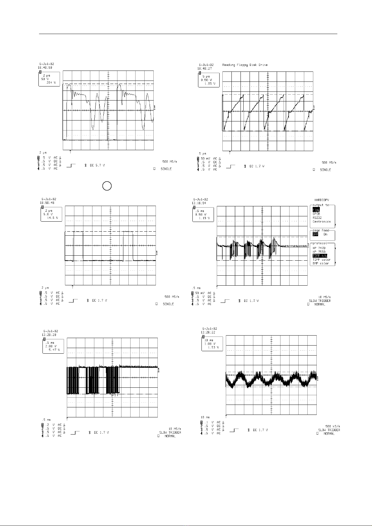
WAVEFORMS OF KEY POINTS
SERVICE MANUAL
Switch Transistor QI’S D on DVD Power PCB
DVD Power PCB N01’s Pin 4
DVD Power PCB N01’s Pin 6
D701’s Pin 3 SCL
D701’s Pin 4 SDA
40
D701’s Pin 6 XT1
Page 42
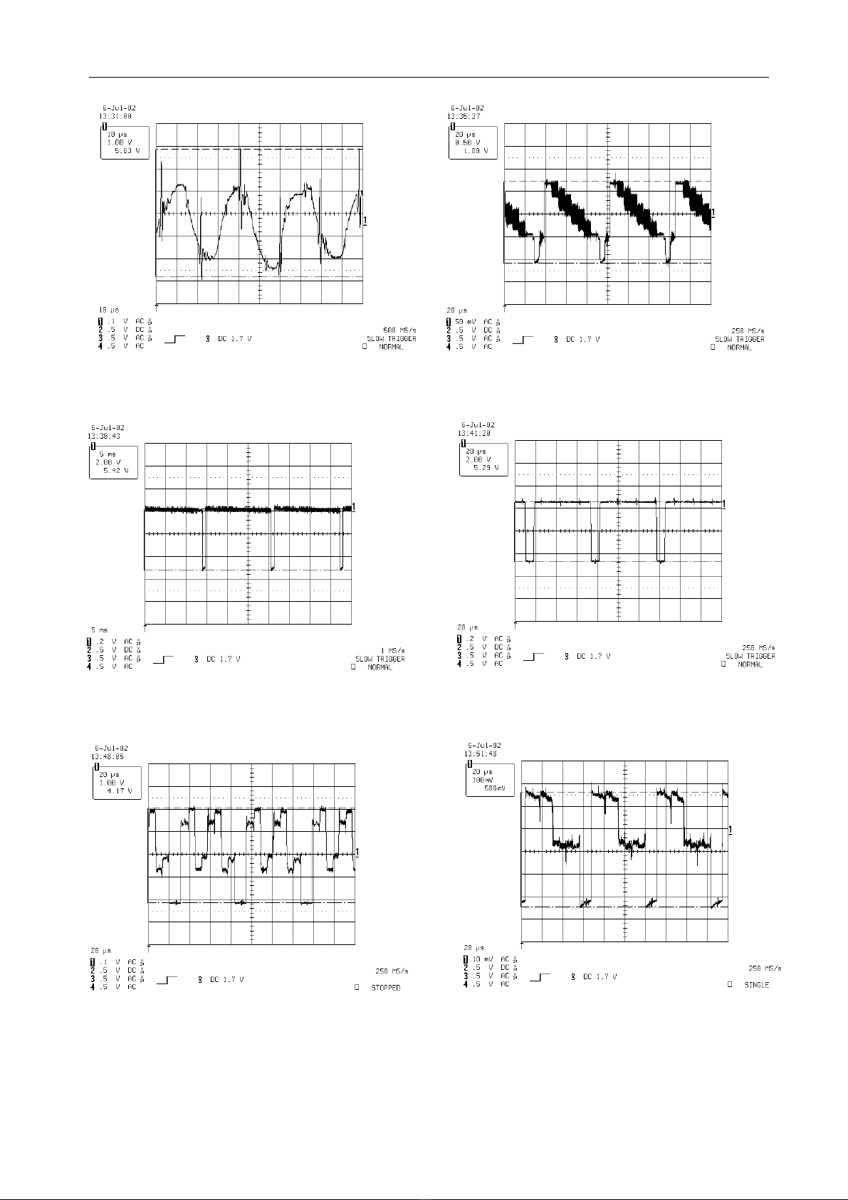
SERVICE MANUAL
D701’s Pin 7 XT2
D701’s Pin 17 V-SYNC
D701’s Pin 15 C-VIN
D701’s Pin 18 H-SYNC
N101’s Pin 19 R-OUT
41
N101’s Pin 20 G-OUT
Page 43
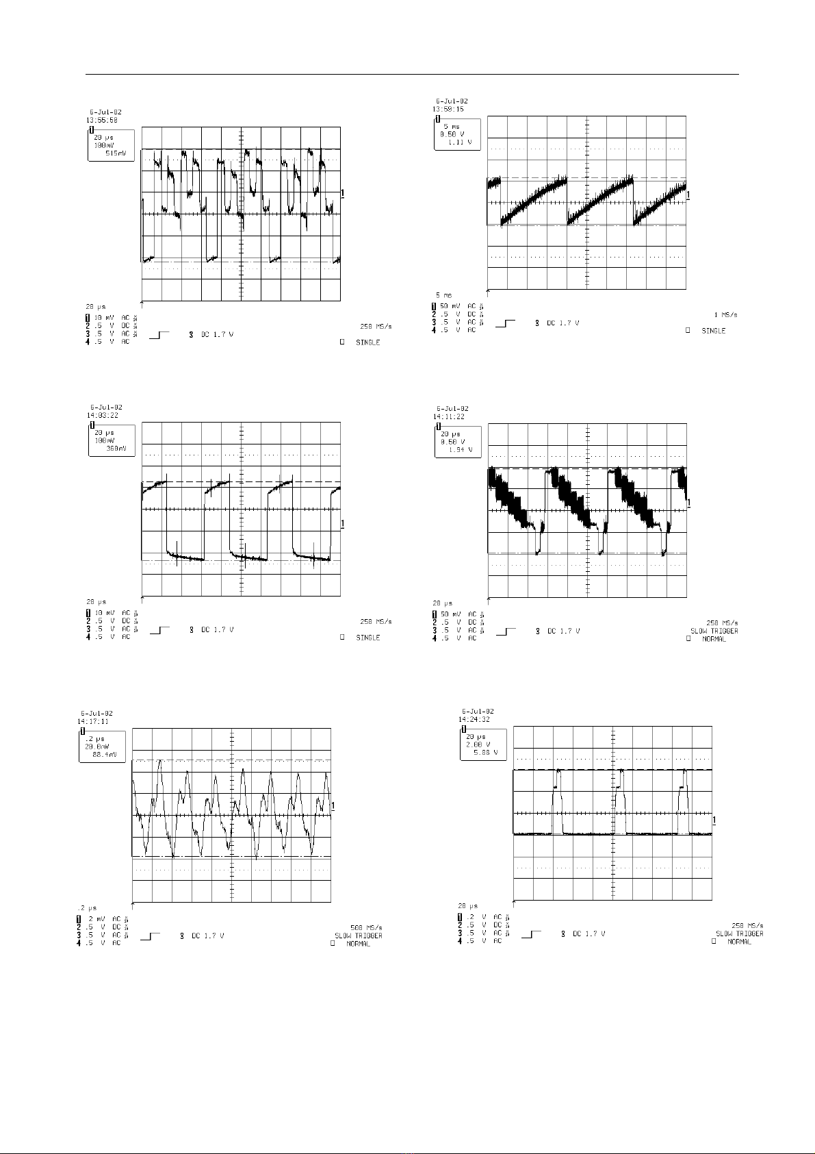
SERVICE MANUAL
N101’s Pin 21 B-OUT
N101’s Pin 27 HOR-OUT
N101’s Pin 23 VER-OUT
N101’s Pin 46 VIDEO-OUT
N101’s Pin 38 X TAL
42
N101’s Pin 28 FBP-IN
Page 44
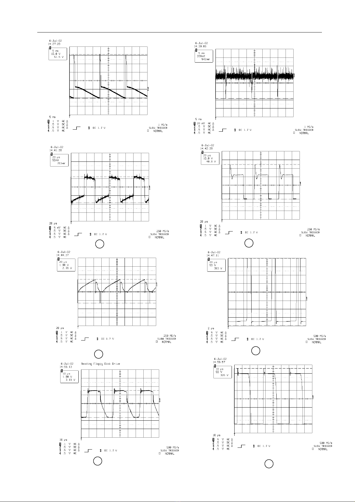
SERVICE MANUAL
N301’s Pin2 VER-OUT
N301’s Pin 5 INVERTING-IN
V431 B
V431 C
V432 B
V432 C
V513 B
43
V513 C
Page 45

SERVICE MANUAL
SERVICE DATA FOR DVD UNIT
TECHNICAL DATA OF KEY ICS
MT1369AE
MPEG decoder/DVD servo processor
1. Features
■ Super lntegration DVD player single chip
· Servo controller and data channel processing
· MPEG-1/MPEG-2/JPEG video decoding
· AC-3/DTS/DVD-Audio/MP3 audio decoding
· Unified track buffer and A/V decoding buffer
· Video processing for scaling and video quality enhancement
· OSD & Sub-picture decoding
· Built-in clock generator
■ Speed Performance on Servo and Decoding
· DVD-ROM up to 8XS
· CD-ROM up to 24XS
· Built-in a frequency programmable clock to μp and RSPO decoder to optimize the
performance over power
■ Channel Data Processor
·
Provides interface with analog front-end processor
· Analog data slicer for small jitter capability
· Built-in high performance data PLL for channel data demodulation
· EFM/EFM+ data demodulation
· Enhanced channel data frame sync protection & DVD-ROM sector sync protection
■ Servo Control and Spindle Motor Control
·
Programmable frequency error gain and phase error gain of spindle PLL to control spindle motor on CLV
and CAV mode
· Provide a varipitch speed control for CLV and CAV mode
· Built-in ADCs and DACs for digital servo control
· Provide 2 general PWM
· Tray control can be PWM output or digital output
· Built-in DSP for digital servo control
■ Host Micro controller
· Built-in 8032 micro controller
· Built-in internal 373 and 8-bit programmable lower address port
· 256-bytes on-chip RAM
· Up to 1M bytes FLASH-programming interface
· Supports 5/3.3-Volt. FLASH interface
· Supports power-down mode
· Supports additional serial port
■ DVD-ROM/CD-ROM Decoding Logic
· Supports CD-ROM Mode 1, CD-ROM XA Mode 2 Form 1, CD-ROM XA Mode 2 Form 2, and CD-DA
formats
45
Page 46

SERVICE MANUAL
· High-speed ECC logic capable of correcting one error per each P-codeword or Q-codeword
· Automatic sector mode and form detection
· Automatic sector header verification
· 8-bit counter for decode completion on ck
· Automatically repeated error corrections
· 8-bit C2 Pointer counter
· Decoder Error Notification Interrupt that signals various decoder errors
· Provide error correction acceleration
■ Buffer Memory Controller
· Supports 16Mb/32Mb/64Mb SDRAM
· Supports 16-bit/32-bit SDRAM data bus interface
· Build in a DRAM interface programmable clock to optimize the DRAM performance
· Provide the self-refresh mode SDRAM
· Programmable DRAM access cycle and refresh cycle timings
· Block-based sector addressing
· Programmable buffering counter for buffer status tracking
· Maximum DRAM speed is 133MHz
· Support 5/3.3-Volt. DRAM Interface
■ Video Decode
· Decodes MPEG1 video and MPEG2 main level,main profile video(720/480 and 720×576)
· Maximum input bit-rate of 15Mbits/sec
· Smooth digest view function with 1, P and B picture decoding
· Baseline, extended-sequential and progressive JPEG image decoding
· Support CD-G titles
■ Video/SPU/HLI Processor
· Arbitrary ratio vertical/horizontal scaling of video, from 0.25X to 256X
· 256/16/4/2-color bitmap format OSD
· 256/16 color RLC format OSD
· Automactic scrolling of OSD image
· Warp mode of OSD can reduce memory required
· Dual Sub-picture decoder
· Provides 4-color/32×32-pixel hardware cursor
· Fade-in,Fade out,and Wipe functions as specified in the DVD Audio Specification and other slide show
transition effects
■ Audio Processing
- Decoder format supports.
- Dolby Digital (AC-3) decoding
- DTS decoding
- MLP decoding for DVD-Audio
- MPEG-1 layer 1/layer 2 audio decoding
46
Page 47
SERVICE MANUAL
- MPEG-2 layer1/layer2 2-channel audio decoding
- Dolby Pro Logic decoding
· Up to 6 channel linear PCM output for DVD Audio/DVD Video
· Downmix function
· Support IEC 60958/61937 output
- PCM/bit stream/mute mode
- Custom IEC latency up to 2 frames
a)
· Pink noise and white noise generator
· Karaoke functions
- Microphone echo with adjustable echo level, echo-depth and delay length
- Microphone tone control with three custom second-order IIR filter
- Vocal mute/vocal assistant
- Key shift up to +/-8 keys controlled by 1/2 key
· Channel equalizer
· 3D surround processing include virtual surround and speaker separation
· Power-down control
· Outline
· 208-pin LQFP package
· 313/216-Volt Dual perating votages
2. Pin Definitions
Pin Symbol Type Description
1 IREF Analog Input
2 PLLVSS Ground Ground for data PLL and related analog circuitry
3 LPIOP Analog Output Positive output of the low pass filter
4 LPION Analog Output Negative output of the low pass filter
5 LPFON Analog Output Negative output of loop filter amplifier
6 LPFIP Analog Input Positive input of loop filter amplifier
7 LPFIN Analog Input Negative input of loop filter amplifier
8 LPFOP Analog Output Positive output of loop filter amplifier
9 JITFO Analog Output RF jitter meter output
10 JITFN Analog Input Negative input of the operation amplifier for RF jigger meter
11 PLLVDD3 Power Power for data PLL and related analog circuitry
12 FOO Analog Output Focus servo output. PDM output of focus servo compensator
13 TRO Analog Output Tracking servo output PDM output of focus servo compensator
14 TROPENPWM Analog Output
15 PWMOUT 2 Analog Output The general PWM output
16 DVD2 Power 2.5V power
17 DMO Analog Output Disk motor control output PWM output
47
Current reference input. It generate reference current for data PLL.
Connect an external 100K resistor to this pin and PLLVSS.
Tray open output, controlled by microcontroller.
This is PWM output for TRWMEN
TRWMEN
27hRW2
=0
=1 or is digital output for
27hRW2
(Continued)
Page 48

SERVICE MANUAL
18 FMO Analog Output Feed motor control. PWM output
19 FG Inout, Pull Up Motor Hall sensor input
20 DVSS Ground Ground
21 HIGHA0 Inout, Pull Up Microcontroller address 8
22 HIGHA1 Inout, Pull Up Microcontroller address 9
23 HIGHA2 Inout, Pull Up Microcontroller address 10
24 HIGHA3 Inout, Pull Up Microcontroller address 11
25 HIGHA4 Inout, Pull Up Microcontroller address 12
26 HIGHA5 Inout, Pull Up Microcontroller address 13
27 DVSS Ground Ground
28 HIGHA6 Inout, Pull Up Microcontroller address 14
29 HIGHA7 Inout, Pull Up Microcontroller address 15
30 AD7 Inout Microcontroller address/data 7
31 AD6 Inout Microcontroller address/data 6
32 AD5 Inout Microcontroller address/data 5
33 AD4 Inout Microcontroller address/data 4
34 DVDD3 Power 3.3V power
35 AD3 Inout Microcontroller address/data 3
36 AD2 Inout Microcontroller address/data 2
37 AD1 Inout Microcontroller address/data 1
38 AD0 Inout Microcontroller address/data 0
39 IOA0 Inout, Pull Up Microcontroller address 0/GPIO0
40 IOA1 Inout, Pull Up Microcontroller address 1/GPIO1
41 DVDD2 Power 2.5V power
42 IOA2 Inout, Pull Up Microcontroller address 2/GPIO2
43 IOA3 Inout, Pull Up Microcontroller address 3/GPIO3
44 IOA4 Inout, Pull Up Microcontroller address 4/GPIO4
45 IOA5 Inout, Pull Up Microcontroller address 5/GPIO5
46 IOA6 Inout, Pull Up Microcontroller address 6/GPIO6
47 IOA7 Inout, Pull Up Micro controller address 7/GPIO7
48 A16 Output Flash address 16
49 A17 Output Flash address 17
50 IOA18 Inout Flash address 18/GPIO10
51 KOA19 Inout Flash address 19/GPIO11
52 DMVSS Ground Ground for DRAM clock circuitry
53 DMVDD3 Power Power for DRAM clock circuitry
54 ALE Inout, Pull Up Microcontroller address latch enable
55 LOOE# Inout Flash output enable, active low/GPIO13
56 LOWR# Inout Flash write enable, active low/GPIO17
57 LOCS# Inout, Pull Up Flash chip select, active low/GPIO18
58 DVSS Ground Ground
59 UP1-2 Inout, Pull Up Microcontroller port 1-2
60 UP1-3 Inout, Pull Up Microcontroller port 1-3
61 UP1-4 Inout, Pull Up Microcontroller port 1-4
(Continued)
48
Page 49

SERVICE MANUAL
62 UP1-5 Inout, Pull Up Microcontroller port 1-5
63 UP1-6 Inout, Pull Up Microcontroller port 1-6
64 DVDD3 Power 3.3V power
65 UP1-7 Inout, Pull Up Microcontroller port 1-7
66 UP3-0 Inout, Pull Up Microcontroller port 3-0
67 UP3-1 Inout, Pull Up Microcontroller port 3-1
68 INT0# Inout, Pull Up Microcontroller interrupt 0, active low
69 IR Input IR control signal input
70 DVDD2 Power 2.5V power
71 UP3-4 Inout Microcontroller port 3-4
72 UP3-5 Inout Microcontroller port 3-5
73 UWR# Inout, Pull Up Microcontroller write strobe, active low
74 URD# Inout, Pull Up Microcontroller read strobe, active low
75 XTALI Input Crystal input, 27MHz
76 XTALO Output Crystal output
77 DVSS Ground Ground
78 RD7 Inout DRAM data 7
79 RD6 Inout DRAM data 6
80 RD5 Inout DRAM data 5
81 RD4 Inout DRAM data 4
82 DVDD2 Power 2.5V power
83 RD3 Inout DRAM data 3
84 RD2 Inout DRAM data 2
85 RD1 Inout DRAM data 1
86 RD0 Inout DRAM data 0
87 RWE# Output DRAM write enable, active low
88 CAS# Output DRAM column address strobe, active low
89 RAS# Output DRAM row address strobe, active low
90 RCS# Output DRAM chip select, active low
91 BA0 Output DRAM bank address 0
92 DVDD3 Power 3.3V power
93 RD15 Inout, Pull Up/Down DRAM data 15
94 RD14 Inout, Pull Up/Down DRAM data 14
95 RD13 Inout, Pull Up/Down DRAM data 13
96 RD12 Inout, Pull Up/Down DRAM data 12
97 DVSS Ground Ground
98 RD11 Inout, Pull Up/Down DRAM data 11
99 RD10 Inout, Pull Up/Down DRAM data 10
100 RD9 Inout, Pull Up/Down DRAM data 9
101 RD8 Inout, Pull Up/Down DRAM data 8
102 VPVDD3 Power Power for varipitch VCO circuitry
103 VCOCIN Analog Input Connect capacitor for compensator loop filter
104 VPVSS Ground Ground for varipitch VCO circuitry
105 DVSS Ground Ground
(Continued)
49
Page 50

SERVICE MANUAL
106 CLK Output DRAM clock
107 CLE Output DRAM clock enable
108 RA11 Output DRAM address bit 11 or audio serial data 3 (channel 3/8)
109 RA9 Output DRAM address 9
110 RA8 Output DRAM address 8
111 DVDD2 Power 2.5V power
112 RA7 Output DRAM address 7
113 RA6 Output DRAM address 6
114 RA5 Output DRAM address 5
115 RA4 Output DRAM address 4
116 DVSS Ground Ground
117 DQM1 Output Mask for DRAM input/output byte 1
118 DQM0 Output Mask for DRAM input/output byte 0
119 BA1 Output DRAM bank address 0
120 RA10 Output DRAM address 10
121 DVDD2 Power 2.5V power
122 RA0 Output DRAM address 0
123 RA1 Output DRAM address 1
124 RA2 Output DRAM address 2
125 RA3 Output DRAM address 3
126 DVSS Ground Ground
127 RD31 Inout, Pull Up/Down DRAM data 31
128 RD30 Inout, Pull Up/Down DRAM data 30
129 RD29 Inout, Pull Up/Down DRAM data 29
130 RD28 Inout, Pull Up/Down DRAM data 28
131 DVDD3 Power 3.3V power
132 RD27 Inout, Pull Up/Down DRAM data 27
133 RD26 Inout, Pull Up/Down DRAM data 26
134 RD25 Inout, Pull Up/Down DRAM data 25
135 RD24 Inout, Pull Up/Down DRAM data 24
136 DVSS Ground Ground
137 DQM3 Output Mask for DRAM input/output byte 3
138 DQM2 Output Mask for DRAM input/output byte 2
139 RD23 Inout, Pull Up/Down DRAM data 23
140 RD22 Inout, Pull Up/Down DRAM data 22
141 DVDD2 Power 2.5V power
142 RD21 Inout, Pull Up/Down DRAM data 21
143 RD20 Inout, Pull Up/Down DRAM data 20
144 RD19 Inout, Pull Up/Down DRAM data 19
145 RD18 Inout, Pull Up/Down DRAM data 18
146 DVSS Guound Ground
147 RD17 Inout, Pull Up/Down DRAM data 17
148 RD16 Inout, Pull Up/Down DRAM data 16
149 ABCK Output Audio bit clock
(Continued)
50
Page 51
SERVICE MANUAL
(1) Audio left/right channel clock
150 ALRCK Inout, Pull Down
151 DVDD3 Power 3.3V power
152 ASDATA0 Inout, Pull Down Audio serial data 0 (left/right channel)
153 ASDATA1 Inout, Pull Down Audio serial data 1 (surround left/surround right channel)
154 ASDATA2 Inout, Pull Down Audio serial data 2 (center/LFE channel)
155 ACLK Inout Audio DAC master clock (384/256 audio sample frequency)
156 APVDD8 Power Power for audio clock circuitry
157 APVSS Ground Ground for audio clock circuitry
158 SPDIE Output SPDIF output
159 MC-DAT Input Miorophone serial input
160 BLANK# Inout Video blank area, active low/GPIO14
161 VSYN Inout Vertical sync/GPIO16
162 HSYN Inout Horizontal sync/GPIO15
163 DVSS Ground Ground
164 YUV0 Output Video data output bit 0
165 YUV1 Output Video data output bit 1
166 YUV2 Output Video data output bit 2
167 YUV3 Output Video data output bit 3
168 YUV4 Output Video data output bit 4
169 DVDD2 Power 2.5V power
170 YUV5 Output Video data output bit 5
171 YUV6 Output Video data output bit 6
172 YUV7 Output Video data output bit 7
173 ICE Input, Pull Down Microcontroller ICE mode enable
174 PRST Input, Pull Down Power on reset input, active high
175 DVSS Ground Ground
176 VFO13 Output The 1st, 3rd VFO pulse output of DVD-RAM ID header
177 IDGATE Output DVD-RAM ID header detect signal output
178 DVDD3 Power 3.3V power
179 UDGATE Output DVD-RAM recording data gate singal output
180 WOBSI Input Wobble signal output
181 SDATA Output RF serial data output
182 SDEN Output RF serial data latch enable
183 SLCK Output RF serial clock output
184 BDO Input, Pull Down Flag of defect data status input
185 DVDD3 Power 3.3V power
186 PDMVDD3 Power Power for PDM circuitry
187 PWMVREF Analog Input A reference voltage input for PWM circuitry. A typical value of 2.8v
188 PWM2VREF Analog Input A reference voltage input for PWM circuitry. A typical value of 1.4v
189 PDMVSS Ground Ground for PDM circuitry
190 ADCVSS Ground Ground for ADC circuitry
191 ADIN Analog Input General AVD input
(2) Trap value in power-on reset.
1:use external 373, 0:use internal 373
(Continued)
51
Page 52
SERVICE MANUAL
192 RFSUBI Analog Input RF subtraction signal input terminal
193 TEZISLV Analog Input Tracking error zero crossing low pass input
194 TEI Analog Input Tracking error input
195 CSO Analog Input Central servo input
196 FEI Analog Input Focus error input
197 RFLEVEL Analog Input Sub beam add input or RFRP low pass input
198 RFRP-DC Analog Input RF ripple detect input
199 RFRP-AC Analog Input RF ripple detect input (through AC coupling)
200 RFRPSLV Analog Input RFRP slice level input
201 HRFZC Analog Input High frequency RF ripple zero crossing
202 ADCVDD8 Power Power for ADC circuitry
203 RADTSI VP Analog Output Positive RF data slicer level output
204 SCON Analog Output Negative analog slicer current output
205 SCOP Analog Output Positive analog slicer current output
206 RFDTSLVN Analog Output Negative RF data slicer level output
207 RFIN Analog Input Negative input of RF differential signal
208 RFP Analog Input Positive input of RF differential signal
52
Page 53

SERVICE MANUAL
MT1336E
RF amplifier
1.General Description
MT1336 is a high performance CMOS analog front-end IC for both CD_ROM driver up to 48XS and
DVD_ROM driver up to 16XS. It also supports DVD_RAM lead up to 4XS Version 2. It contains servo
amplifiers to generate focusing error, 3-beam tracking error, 1 beam radial push-pull signal, RF level and
SBAD for servo functions. It also includes DPD tracking error signal for DVD_ROM application. For
DVD_RAM disks, there are also Differential Push-Pull (DPP) method for generating tracking signal and
Differential Astigmatic Detection (DAD) for processing focusing signal. Programmable equalizer and AGC
circuits are also incorporated in this chip to optimize read channel performance. In addition, this chip has
dual automatic laser power control circuits for DVD-ROM (DVD-RAM) and CD-ROM separately and
reference voltage generators to reduce external components. Programmable functions are implemented by
the access of internal register through bi-directional serial port to configure modes selection.
2. Features
· RF equalizer with programmable fc from 3MHz to 70MHz and programmable boost from 3dB to 13dB.
· MT1336 supports at least eight different kinds of pick-up heads with versatile input configuration for both
RF input stages and servo signal blocks.
· 3 beams tracking error signal generator for CD_ROM application.
· One beam differential phase tracking error (DPD) generator for DVD_ROM application.
· Differential push pull tracking error (DPP) generator for DVD_RAM application.
· Focusing error signal generator for CD-ROM, DVD-ROM and DVD-RAM (DAD method).
· RF level signal generator.
· Sub-beam added signal for 3 beams CD-ROM.
· One beam push-pull signal generator for central servo application.
· High speed RF envelop detection circuit with bandwidth up to 400KHz for CD-ROM.
· Defect and Blank detection circuits.
· Dual automatic laser power control circuits with programmable level of LD monitor voltage.
· Vref=1.4V voltage and V2ref=2.8V voltage generators.
· V20=2.0V voltage for pick-up head reference.
· Bi-directional serial port to access internal registers.
· 128-pin LQFP.
53
Page 54
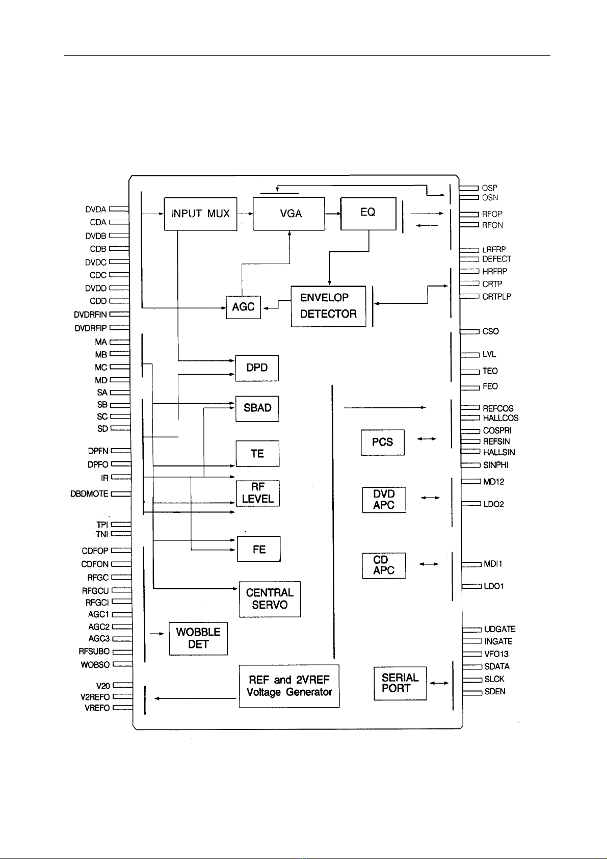
3. block Diagram
SERVICE MANUAL
Fig17. MT1336 Function Block Diagram
54
Page 55
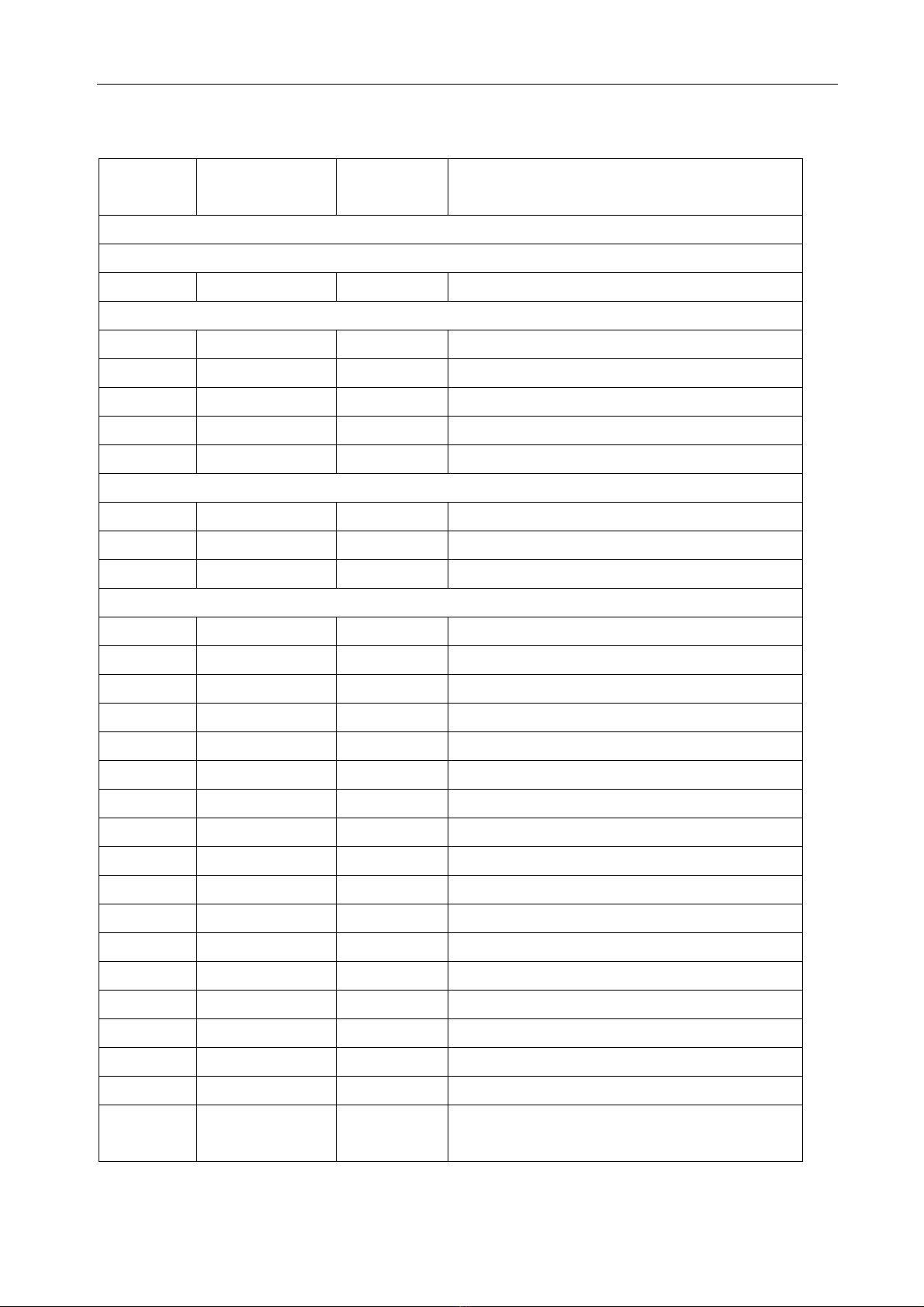
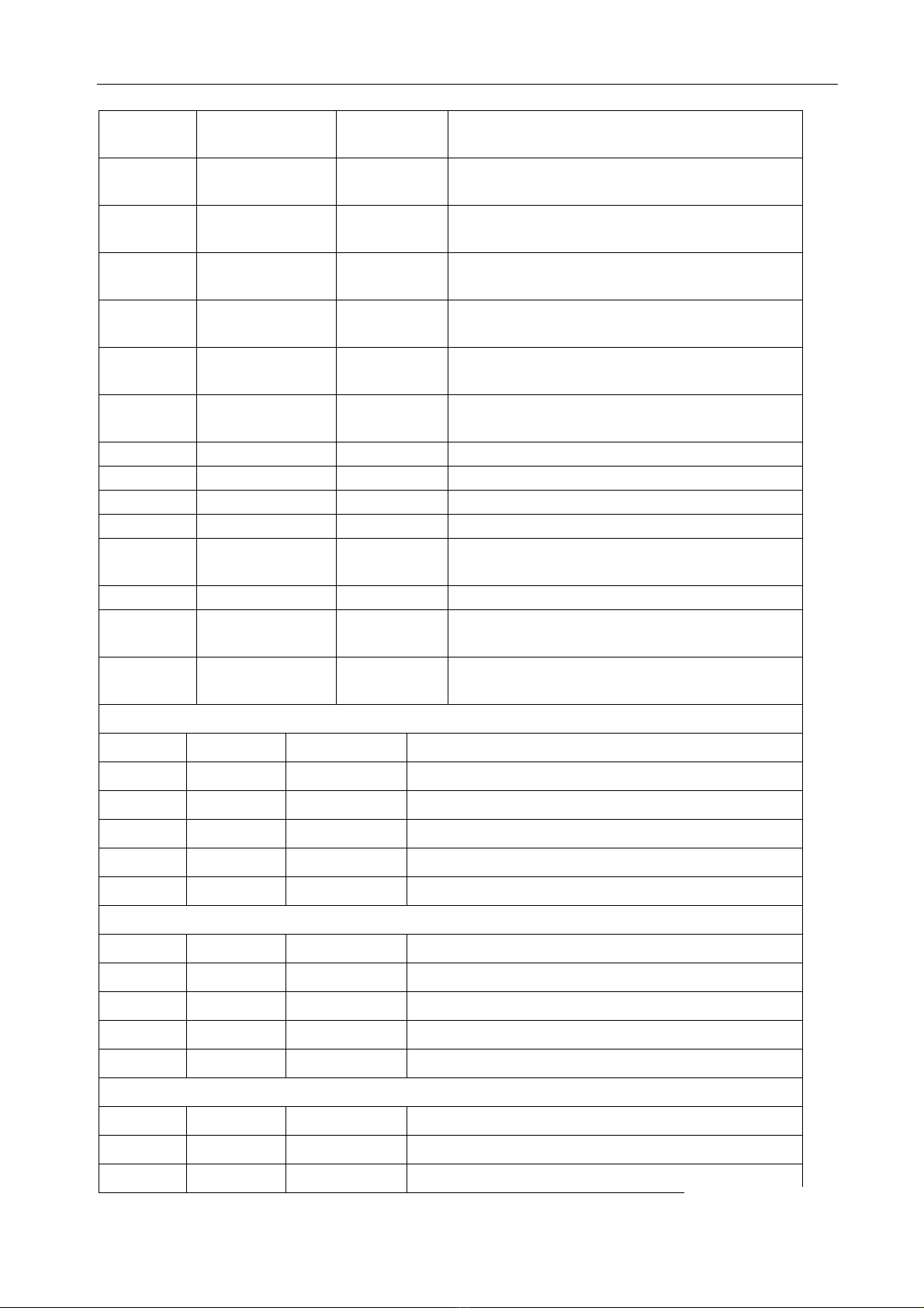
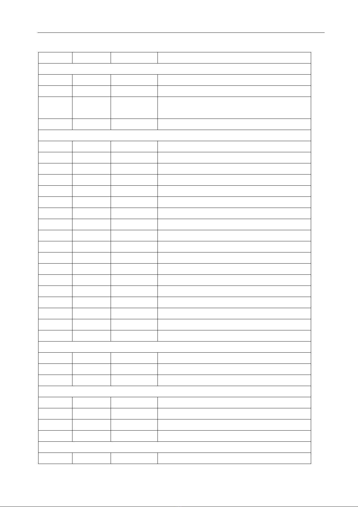
4.MT1336 Pin Descriptions
SERVICE MANUAL
Pin
Symbol Type Description
Numbers
LQFP128
RF Flag Interface
23 DEFECT Digital Output Flag of bad data output status
RF SIO interface
56 SCLK Digital Input RF serial clock input
58 SDEN Digital Input RF serial data input
59 SDATA Digital IO RF serial data IO
60 RST Digital Input Reset(active high)
55 XCK16M Digital Input 16.9MHz for verification
RF SERVO interface
40 UOG ATE Digital Input Control signal for DVD-RAM
41 GGATE Digital Input Control signal for DVD RAM
38 VFO13 Digital Input DVD-RAM Header signal
RF
100 DVDA Analog Input AC coupled DVD RF signal input A
99 DVDB Analog Input AC coupled DVD RF signal input B
98 DVDC Analog Input AC coupled DVD RF signal input C
97 DVDD Analog Input AC coupled DVD RF signal input D
95 DVDRFIN Analog Input AC coupled DVD RF signal input RFIN
96 DVDRFIP Analog Input AC coupled DVD RF signal input RFIP
94 CDA Analog Input AC coupled CD RF signal input A
93 CDB Analog Input AC coupled CD RF signal input B
92 CDC Analog Input AC coupled CD RF signal input C
91 CDD Analog Input AC coupled CD RF signal input D
90 OSN Analog RF offset cancellation capacitor connecting
89 OSP Analog RF offset cancellation capacitor connecting
85 CEQP Analog RF offset cancellation capacitor connecting
84 CEQN Analog RF offset cancellation capacitor connecting
88 RFGC Analog RF AGC loop capacitor connecting for DVD-ROM
87 RFGCU Analog RF AGC loop capacitor connecting for DVD-RAM
86 RFGCU Analog RF AGC loop capacitor connecting for DVD-RAM
DC coupled DVD-RAM main-beam RF signal
101 MA Analog Input
input A
55
(Continued)
Page 56
SERVICE MANUAL
102 MB Analog Input
103 MC Analog Input
104 MD Analog Input
105 SA Analog Input
106 SB Analog Input
110 SC Analog Input
111 SD Analog Input
DC coupled DVD-RAM main-beam RF signal
input B
DC coupled DVD-RAM main-beam RF signal
input C
DC coupled DVD-RAM main-beam RF signal
input D
DC coupled DVD-RAM sub-beam RF signal input
A
DC coupled DVD-RAM sub-beam RF signal input
B
DC coupled DVD-RAM sub-beam RF signal input
C
DC coupled DVD-RAM sub-beam RF signal input
D
108 IR Analog External current bias resistor (R=20K)
119 AGC1 Analog Wobble AGC loop1 capacitor
121 AGC2 Analog Wobble AGC loop2 capacitor
122 AGC3 Analog Wobble AGC loop3 capacitor
127 RFSUBO
Analog
Output
Header push-pull RF output signal
V OBSO Digital Output Wobble signal output
5 RFOP
7 PFON
Analog
Output
Analog
Output
RF positive output
RF negative output
TRACKING ERROR
32 DPFN Analog DPD amplifier negative input
33 DPFO Analog DPD amplifier output
61 DPDMUTE Digital Input DPD mute control input
116 TNI Analog Input 3 beam satellite PD signal negative input E
115 TPI Analog Input 3 beam satellite PD signal negative input F
21 TEO Analog Output Tracking error output
FOCUSING ERROR & RF LEVEL & CENTRAL SERVO SIGNAL
112 CDFOP Analog Input CD focusing error positive input
113 CDFON Analog Input CD focusing error negative input
18 FEO Analog Output Focusing error output
19 LVL Analog Output RF level output
20 CSO Analog Output Central servo signal output
ALPC
124 MDI1 Analog Input Laser power monitor input
125 LDO1 Analog Output Laser driver output
123
56
MDI2 Analog Input Laser power monitor input
(Continued)
Page 57
SERVICE MANUAL
126 LDO2 Analog Output Laser driver output
RF RIPPLE
26 CRTP Analog RF top envelop filter capacitor connecting
27 CRTPLP Analog Defect level filter capacitor connecting
25 HRFRP Analog output
High frequency RF ripple output or Blank detector’s
output
24 LRFRP Analog output Low frequency RF ripple output
POWER
67, 69 AVDD Power Master PLL filter power
65, 73 AGND GND GND for Master PLL filter
64 AVDD Power DPD Power
62 AGND GND DPD GND
109 AVDD Power RF path Power
107 AGND GND RF path GND
114 SVDD Power Servo Power
117 SGND GND Servo GND
2,120 WAVDD Power Wobble Power
128, 118 WAGND GND Wobble GND
5 AVDDO Power Power for RF output
8 AGNDO GND GND for RF output
14 AVDDT Power Power for trimming PAD
12 AGNDT GND GND for trimming PAD
22 VDDP Power Peak Detection Power
31 GNDP GND Peak Detection GND
37, 54 VDD Power Serial I/O Power
39, 57 GND GND Serial I/O GND
REFERENCE VOLTAGE
16 VREFO Analog output Reference voltage 1.4V
15 V2REFO Analog output Reference voltage 2.8V
17 V20 Analog output Reference voltage 2.0V
ALPC TRIMMING
9 TM1 Analog input Trimming pin for ALPC1
10 TM2 Analog input Trimming pin for ALPC1
11 TM3 Analog input Trimming pin for ALPC2
13 TM4 Analog input Trimming pin for ALPC2
HIGH SPEED TRACK COUNTING
29 TRLP Analog Low-pass filter capacitor connecting
57
(Continued)
Page 58
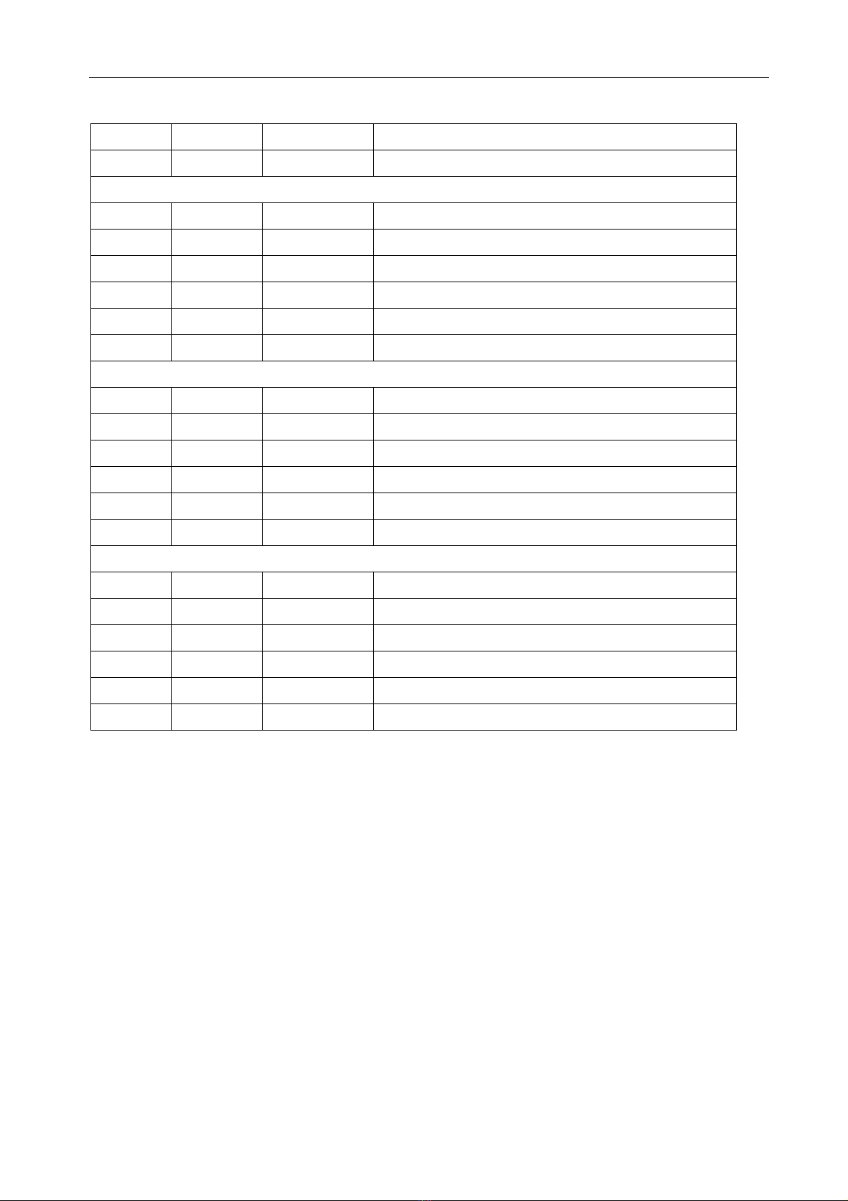
SERVICE MANUAL
28 TRLPA Analog Low-pass filter capacitor connecting
30 HTRC Digital output High speed track counting digital output
PCS
74 HALLSIN Analog input Negative input of amplifier for hall sensor signal
75 REFSIN Analog input Positive input of amplifier for hall sensor signal
76 SINPHI Analog output Amplifier output for hall sensor signal
71 HALLCOS Analog input Negative input of amplifier for hall sensor signal
72 REFCOS Analog input Positive input of amplifier for hall sensor signal
70 COSPHI Analog output Amplifier output for hall sensor signal
FOR MONITOR ONLY
81 MON Analog output
80 MOP Analog output
66 VCON Analog output
77 SWO Analog output Output from mux of SW1 & SW2
78 SW2 Analog input External input for servo input select
79 SW1 Analog input External input for servo input select
FOR SERIAL I/O
42 IO0
43 IO1
44 IO2
45 IO3
46 IO4
47 IO5
58
Page 59
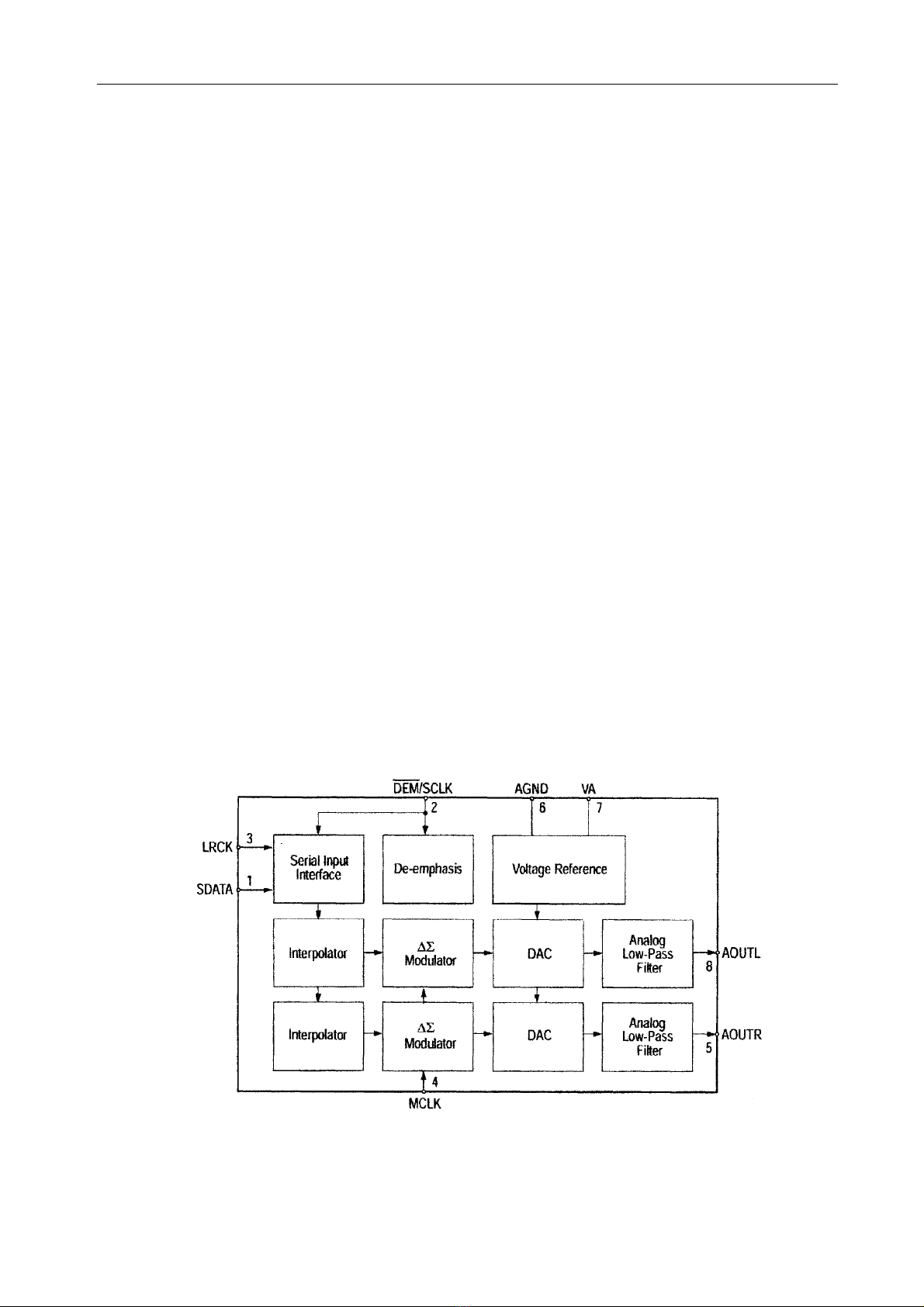
SERVICE MANUAL
CS4334
Audio D/A Controller
1. Features
● Complete Stereo DAC System:
Interpolation, D/A, Output Analog Filtering
● 24-Bit Conversion
● 96 dB Dynamic Range
● –88 dB THD+N
● Low Clock jitter Sensitivity
● Single +5V Power Supply
● Filtered Line Level Outputs
● On-Chip Digital De-emphasis
● Popguard
● Functionally Compatible with
CS4330/31/33
3. Block Diagram
TM
Technology
2. Description
The CS4334 family members are complete,
stereo digital-to-analog output systems including
interpolation, 1-bit D/A conversion and output
analog filtering in an 8-pin package. The
CS4334/5/6/7/8/9 support all major audio data
interface formats, and the individual devices differ
only in the supported interface format.
The CS4334 family is based on delta-sigma
modulation, where the modulator output controls
the reference voltage input to an ultra-linear
analog low-pass filter. This architecture allows for
infinite adjustment of sample rate between 2 kHz
and 100 kHz simply by changing the master clock
frequency.
The CS4334 family contains on-chip digital
de-emphasis, operates from a single +5V power
supply, and requires minimal support dircuitry.
These features are ideal for set-top boxes, DVD
players, SVCD players, and A/V receivers.
Fig.18
59
Page 60
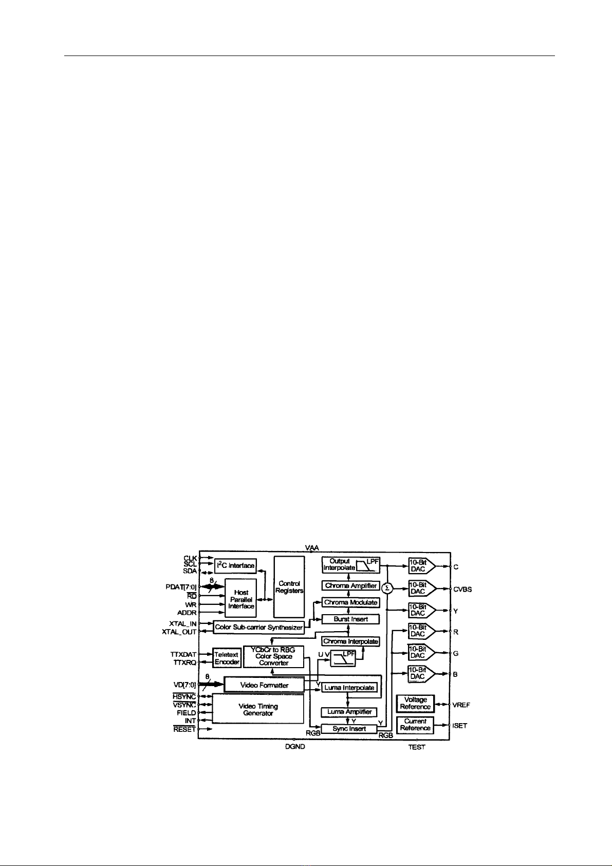
SERVICE MANUAL
CS4955
Video Encoder
1. Features
●Six DACs providing simultaneous
composite, S-Video, and RGB or Component
YUV outputs
●Programmable DAC output currents for low
impedance (37.5 Ω) and high impedance
(150Ω) loads.
● Multi-standard support for NTSC-M,
NTSC-JAPAN, PAL (B, D, G, H, I, M, N,
Combination N)
●ITU R.BT656 input mode supporting
EAV/SAV codes and CCIR601 Master/Slave
input modes
●Programmable HSYNC and VSYNC timing
Multistandard Teletext (Europe, NABTS,
WST) support
●VBI encoding support
●Wide-Screen Signaling (WSS) support, EIA-J
CPX1204
●NTSC closed caption encoder with interrupt
●CS4955 supports Macrovision copy
protection Version 7
●Host interface configurable for parallel or I
2
C
compatible operation
●On-chip voltage reference generator
●+3.3 V or +5V operation CMOS. low-power
modes, tri-state DACs
3. Block Diagram
2. Description
The CS4954/5 provides full conversion from digital
video formats YCbCr or YUV into NTSC and PAL
Composite, Y/C (S-Video) and RGB, or YUV analog
video. Input formats can be 27 MHz 8-bit YUV, 8-bit
YCbCr, or ITU R.BT656 with support for EAV/SAV
codes. Video output can be formatted to be
compatible with NTSC-M, NTSC-J, PAL-B, D, G, H, I,
M, N, and combination N systems. Closed Caption is
supported in NTSC. Teletext is supported for NTSC
and PAL.
Six 10-bit DACs provide two channels for an S-Video
output port, one or two composite video outputs, and
three RGB or YUV outputs. Two-times oversampling
reduces the output filter requirements and
guarantees no DAC-related modulation components
within the specified bandwidth of any of the
supported video standards.
Parallel or high-speed I
2
C compatible control
interfaces are provided for flexibility in system
design. The parallel interface doubles as a general
purpose I/O port when the CS4954/5 is in I
2
C mode
to help conserve valuable board area.
Package:
CS4954CQ/CS4955CQ 48-Pin TQFP
Fig. 19
60
Page 61
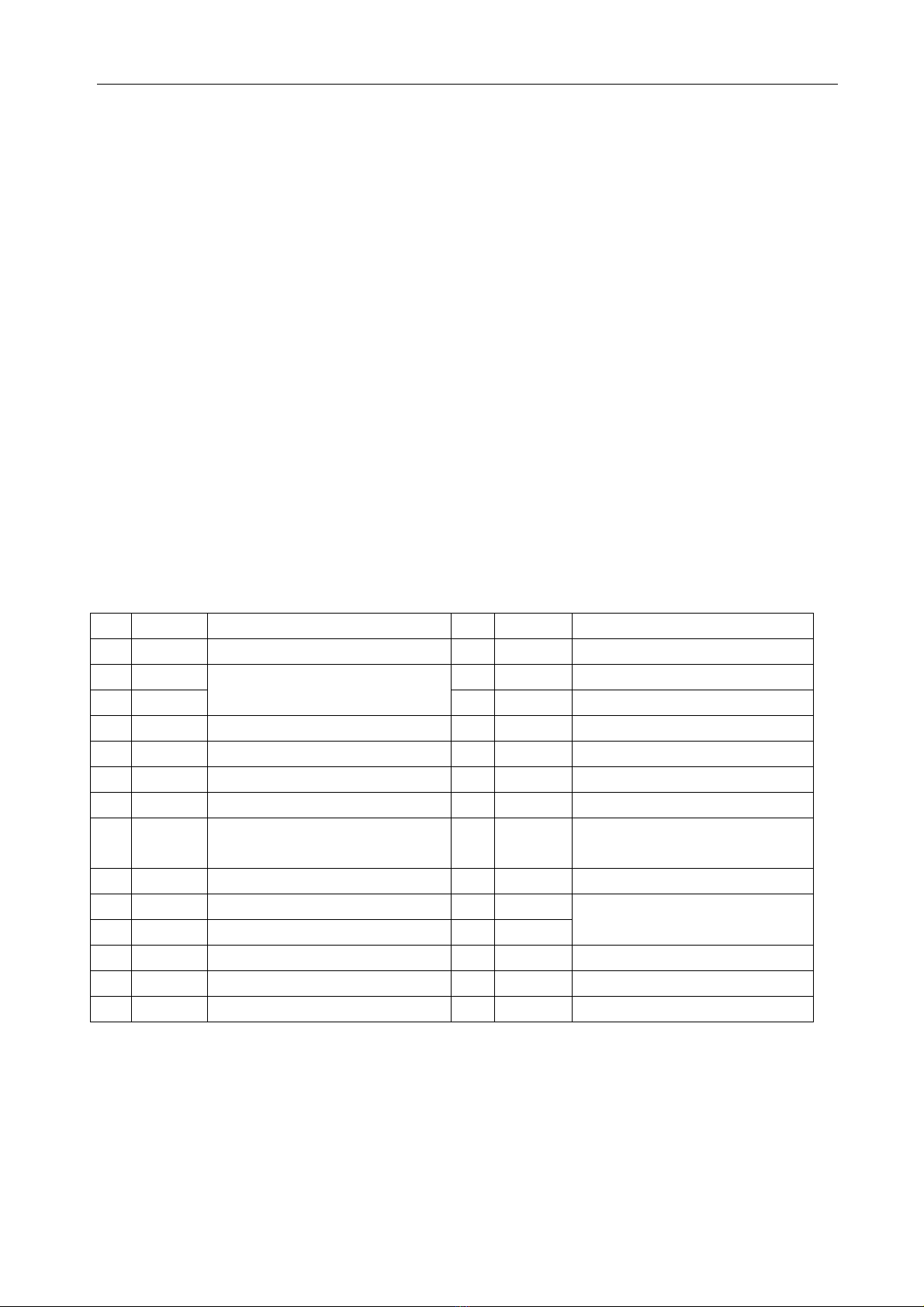
SERVICE MANUAL
BA5954
Focus/tracking Coil and Feed Motor Drive
1. Functions
BA5954FM is a 4 channel driver for optical disc motor driver. Dual channel current feedback type
drivers are built in, in addition to dual channel motor drivers.
Wide dynamic range (4.0V (typ.) at PreVcc=12V, PVcc=5V, RL=8Ω)
Separating Vcc into Pre+Power of sled motor, Power of loading motor and Power of actuator, can make
better power efficiency, by low supply voltage drive.
Level shift circuit built in.
Thermal-shut-down circuit built in.
Stand-by mode built in.
<Actuator driver>
Current phase lag influenced load inductance is little, because this type is current feedback.
< Sled motor driver >
Input pins consist of (+) and (-), therefore various input types are available such as differential input.
<Loading driver >
This is a single input linear BTL driver.
2. Pin Description
No. Symbol Function No. Symbol Function
1 VINFC Input for focus driver 15 VOTK+ Non inverted output of tracking
2 CFCerr1 16 VOTK- Inverted output of tracking
3 CFCerr2
4 VINSL+ Non inverting input for Op-amp 18 VOLD- Inverted output of loading
5 VINSL- Inverting input for OP-amp 19 PGND GND for power block
6 VOSL Output of OP-amp 20 VNFTK Feedback for tracking driver
7 VNFFC Feedback for focus driver 21 PVcc2 Vcc for power block of actuator
8 Vcc
9 PVcc1 Vcc for power block of loading 23 VINLD Input for loading driver
10 PGND GND for power block 24 CTKerr2
11 VOSL- Inverted output of sled 25 CTKerr1
12 VOSL+ Non inverted output of sled 26 VINTK Input for tracking driver
13 VOFC- Inverted output of focus 27 BIAS Input for reference voltage
14 VOFC+ Non inverted output of focus 28 STBY Input for stand-by control
Notes: Symbol of + and – (output of drivers) means polarity to input pin.
(For example if voltage of Pin1 is high, Pin14 is high.)
Connection with capacitor
for error amplifier
Vcc for pre-drive block and
power block of sled
17 VOLD+ Non inverted output of loading
22 PreGND GND for pre-drive block
Connection with capacitor
for error amplifier
61
Page 62
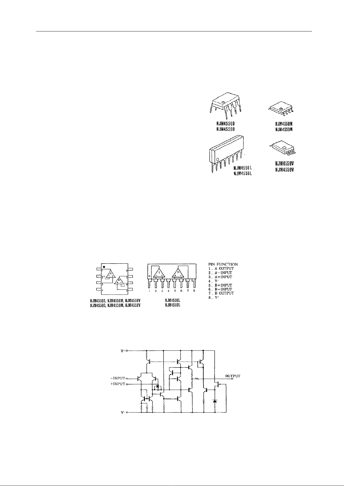
SERVICE MANUAL
NJM4558M
Sound Amplifier
1. General Description
The NJM4558/4559 integrated circuit are a dual high-gain
operational amplifier internally compensated and constructed
on a single silicon chip using an advanced epitaxial process.
Combining the features of the NJM741 with the close
parameter matching and tracking of a dual device on a
monolithic chip results in unique performance characteristics.
Excellent channel separation allow the use of the dual device
in single NJM741 operational amplifier applications providing
density. It is especially well suited for applications in
differential-in, differential-out as well as in potentiometric
amplifiers and where gain and phase matched channels are
mandatory.
2. Features
● Operating Voltage ( ±4V~±18V )
● High Voltage Gain ( 100dB typ. )
● High Input Resistance ( 5MΩ typ. )
● Rackage Outline DIP8. DMP8. SIP8. SSOP8
● Bipolar Technology
3. Pin Configuration
4. Equivalent Circuit (1/2 Shown)
Fig. 21
Fig. 22
5. Package Outline
24C01
62
Fig. 20
Page 63
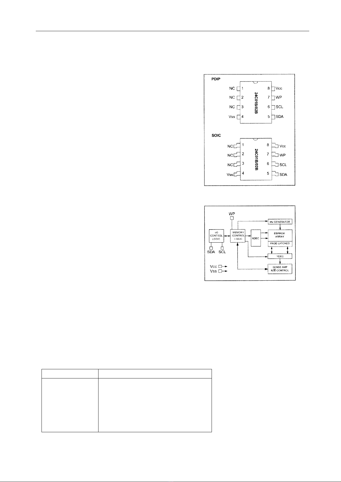
SERVICE MANUAL
1K EEPROM
1. Features
● Single supply with 5.0V operation
● Low power CMOS technology
- 1 mA active current typical
- 10 μA standby current typical at 5.0V
- 5μA standby current typical at 5.0V
● Organized as a single block of 128 bytes (128×8)
or 256 bytes (256×8)
● 2-wire serial interface bus, I
● 100KHz compatibility
● Self-timed write cycle(including auto-erase)
● Page-write buffer for up to 8 bytes
● 2 ms typical write cycle time for page-write
● Hardware write protect for entire memory
● Can be operated as a serial ROM
● ESD protection > 3,000V
● 1,000,000 ERASE/WRITE cycles guaranteed
Data retention > 200 years
● 8 pin DIP or SOIC package
● Available for extended temperature ranges
- Automotive(E) -40℃ to +125℃
2. Description
The Microchip Technology Inc. 24C01B and
24C02B are 1K bit and 2K bit Electrically Erasable
PROMs The devices are organized as a single block
of 128×8 bit or 256×8 bit memory with a 2-wire
serial interface. The 24C01B and 24C02B also have
page-write capability for up to 8 bytes of data. The
24C01B and 24C02B are available in the standard
8-pin DIP and an 8-pin surface mount SOIC package.
These devices are for extended temperature applications
only. It is recommended that all other applications use
Microchip’s 24LC01B/02B.
Pin Function Table
Name Function
Vss
SDA
SCL
WP
Vcc
NC
Ground
Serial Address/Data I/O
Serial Clock
Write Protect Input
+5.0V Power Supply
No Internal Connection
2
C compatible
3. Package Types
4. Block Diagram
Fig. 23
63
Page 64
SERVICE DATA OF KEY ICS
Table 14 Service Data of Key ICs
SERVICE MANUAL
Position Pin No.
Digital Multimeter
Operating Voltage (V)
U1 (MT1336E)
7 RF signal 0.9-1.5V
P-P
2,5,14,64,67,69,109,114,120 5
16,41,70,82,111,121,141,169 2.5
U3 (MT1369AE)
U7 (8M FLASH)
11,34,53,64,92,102,131,151,
156, 178,185,186,202
3.3
12 0
14 Non-cyclical pulse
8 10.6
U21 (BA5954)
9,21 5
11,12,13,14,15,16,17,18 2.5
64
Page 65
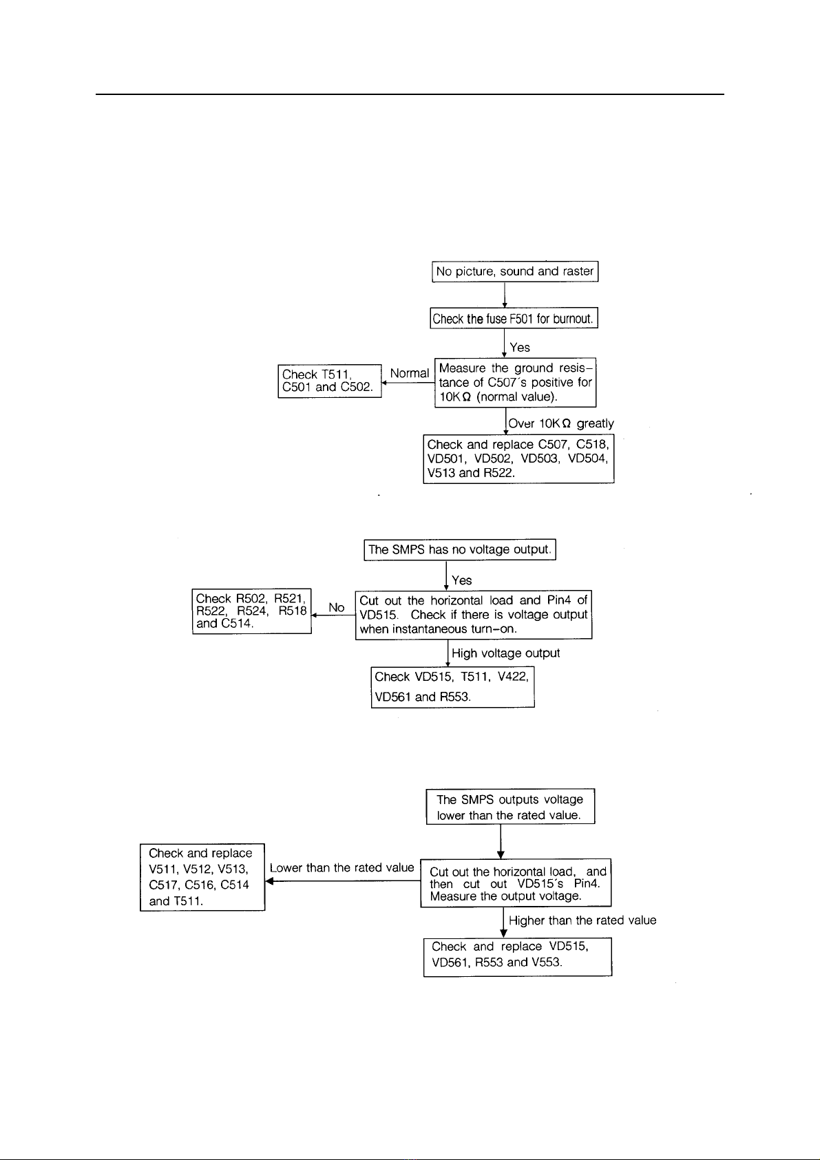
SERVICE MANUAL
TROUBLESHOOTING FLOW CHARTS
TROUBLESHOOTING FLOW CHARTS FOR TV UNIT
1. Switch Mode Power Supply
1.1 No picture, sound and raster
1.2 The SMPS has no voltage output.
1.3 The SMPS outputs voltage lower than the rated value.
65
Page 66
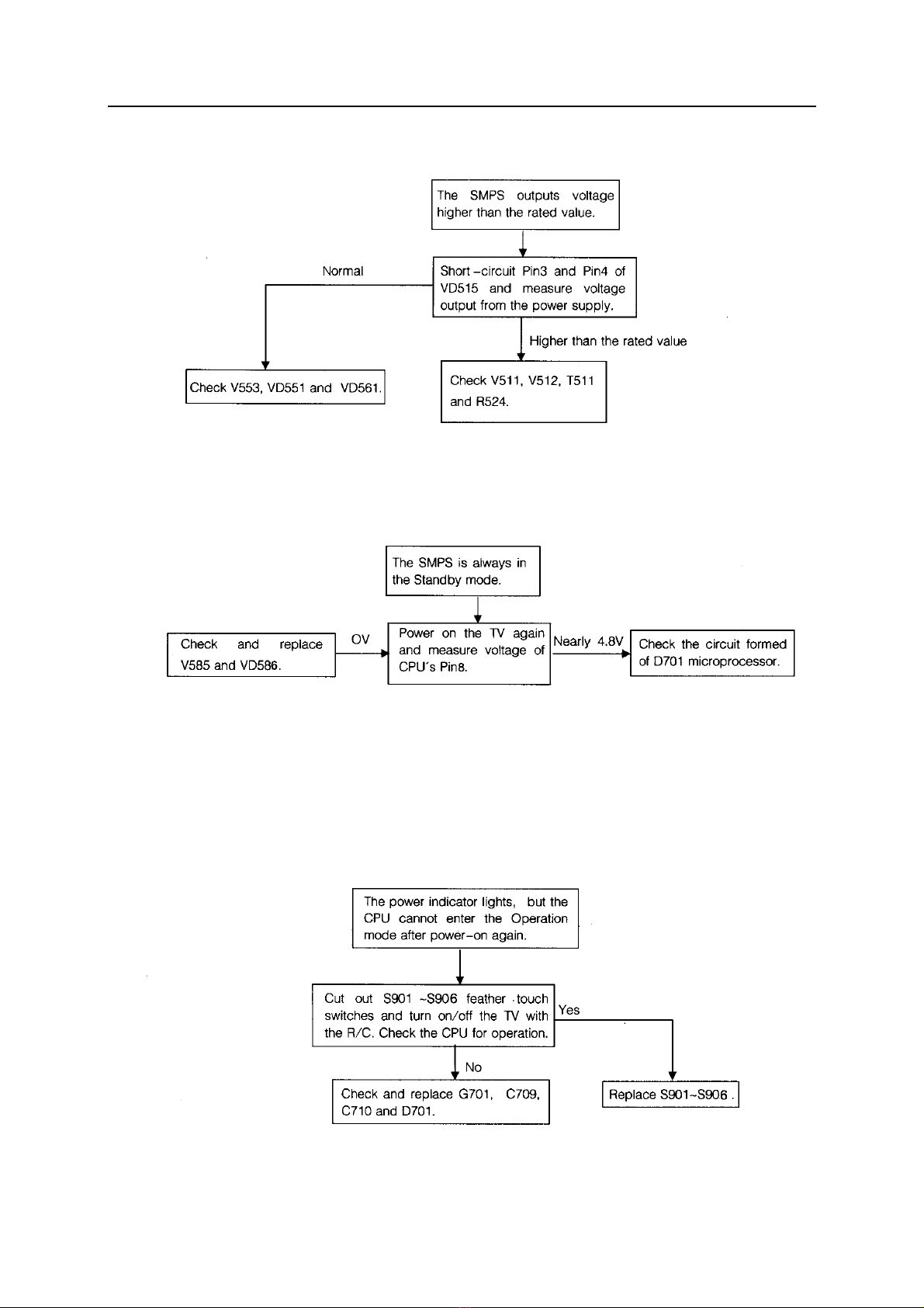
SERVICE MANUAL
1.4 The SMPS outputs voltage higher than the rated value.
1.5 The power indicator lights, but the SMPS is still in the Standby mode.
2. Control System
2.1 The power indicator lights, but the CPU cannot enter the Operation mode
after power-on again
.
66
Page 67
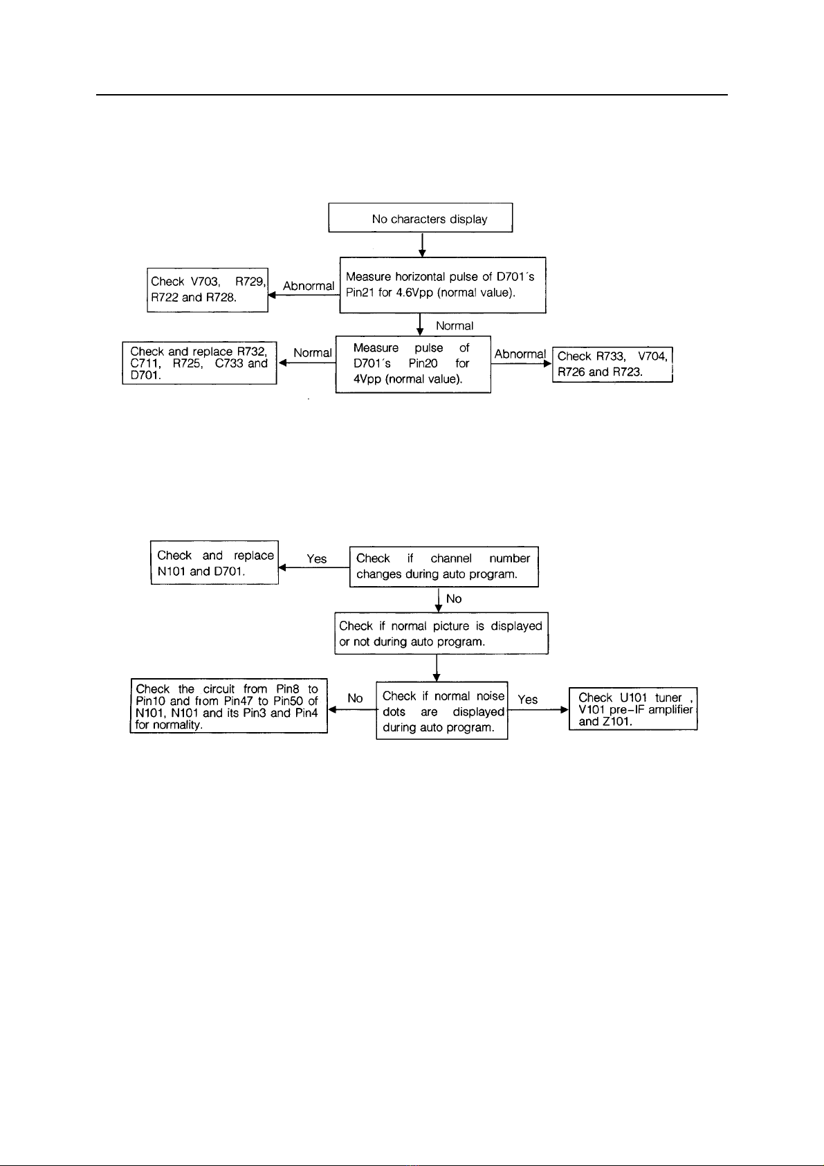
SERVICE MANUAL
2.2 No characters display
2.3 Channel number remains unchanged during auto program.
67
Page 68
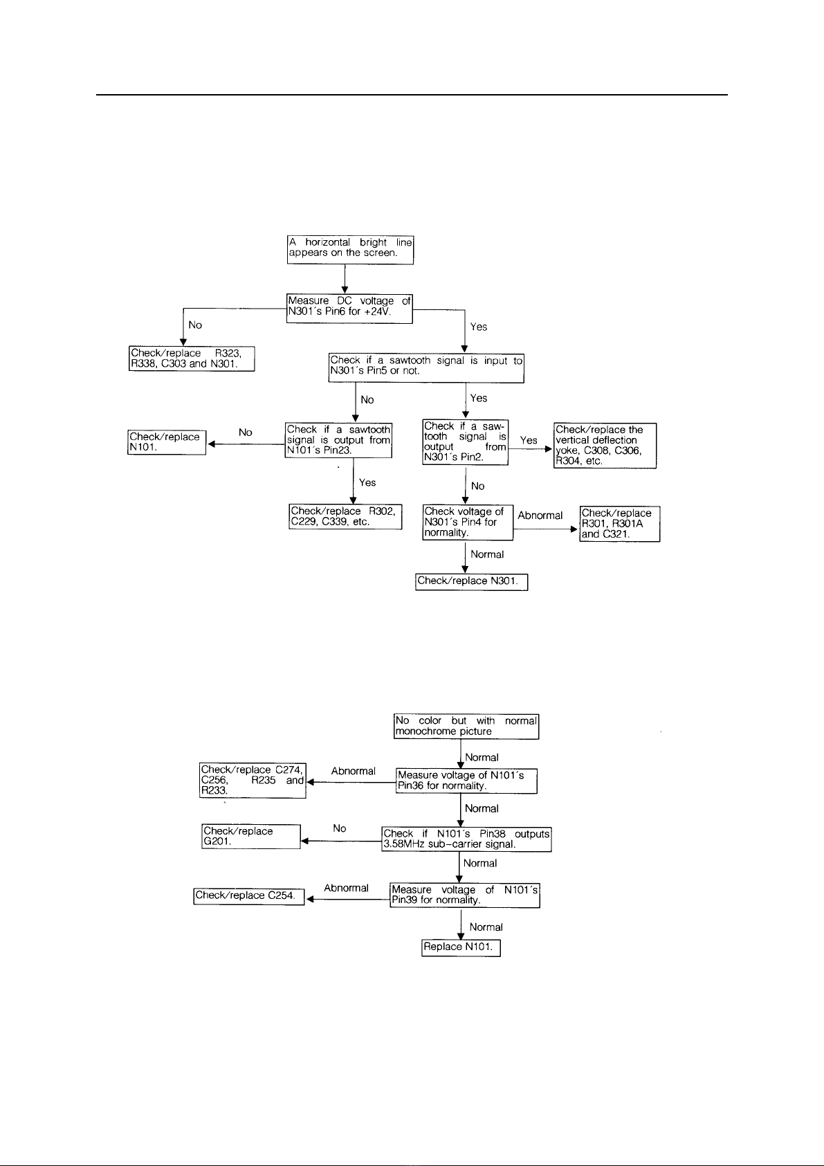
SERVICE MANUAL
3. Video Signal Processor
3.1 A horizontal bright line appears on the screen.
3.2 No color but with normal monochrome picture
68
Page 69
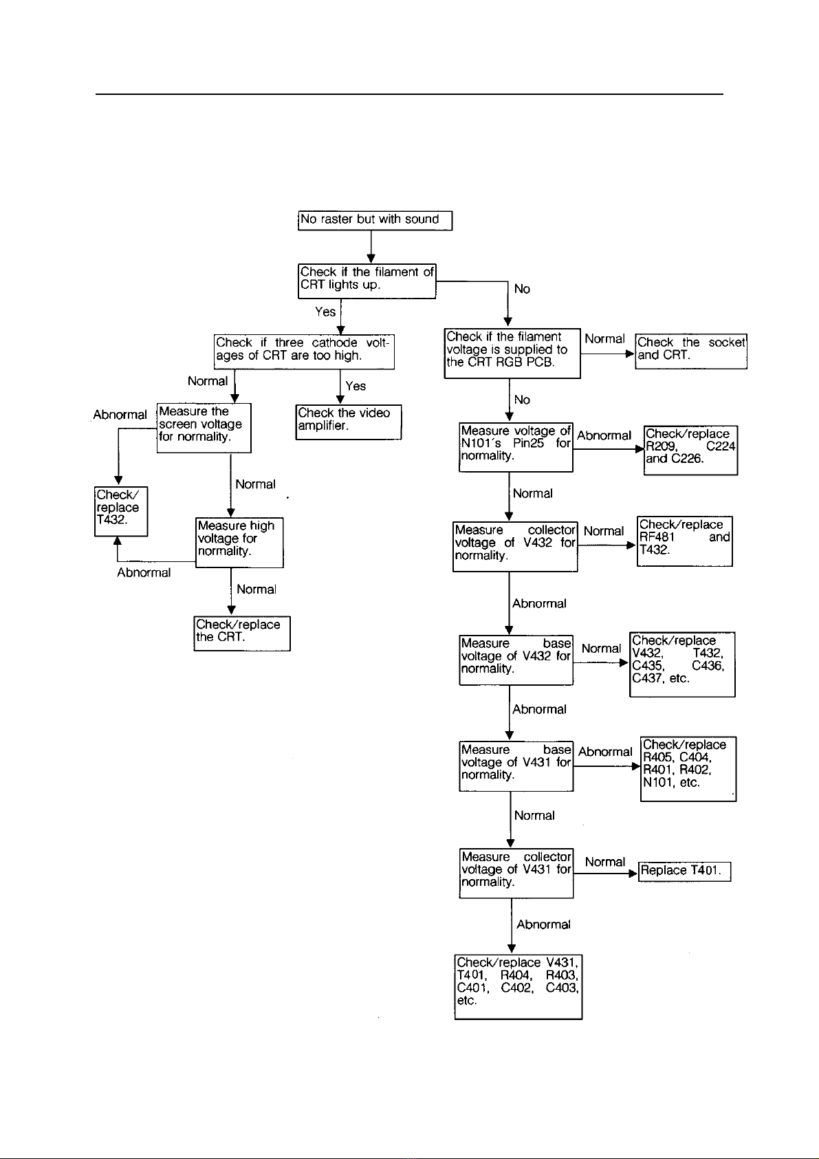
SERVICE MANUAL
4. Horizontal/Vertical Scan Circuit
4.1 No raster but with sound
69
Page 70
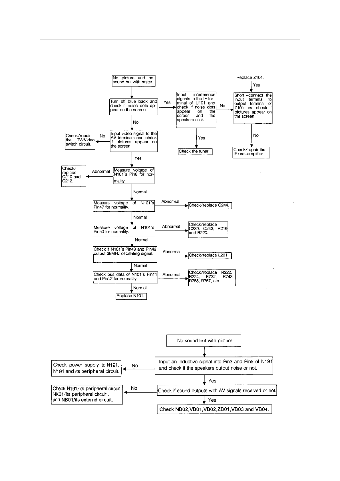
SERVICE MANUAL
4.2 No picture and no sound but with raster
5. Audio System
No sound
70
Page 71
SERVICE MANUAL
TROUBLESHOOTING FLOW CHARTS FOR DVD UNIT
Debugging begins.
AC power comes up to
the power PCB input
standard?
YES
Supply power to the
power PCB separately.
All voltages from the
power PCB conform to
the requirements?
YES
Supply power to the
DEMO PCB after no
short circuit confirmed.
Check the output
voltages +3.3V and
+2.5V from the DEMO
PCB for normality.
NO
NO
NO
Replace the power PCB.
Repair or replace the
power PCB until the
voltage output meets the
requirements.
Detect regulators or
diodes of the two sets of
power to get normal
voltage output.
YES
Connect the unit to a
computer and
program FLASH on
the DEMO PCB
1) Test frequency and amplitude of the
main clock.
2) Check the system RESET circuit for
Programming of
FLASH succeeded?
NO
YES
normality.
3) Check the read enabling lines FRD
and FWR of FLASH for normality.
4) Check RS232 signal for normality.
5) Check the peripheral circuit of
FLASH.
A
71
Page 72
A
Reset or power on again.
SERVICE MANUAL
LOGO display or not?
YES
NO
Access to FLASH
normally?
YES
SDRAM works normally?
YES
Check the data received
by the TV encoder for
correctness.
YES
The TV encoder outputs
normally?
YES
Check connections
between the video
filter/video AMP and the
TV.
NO
NO
NO
NO
Check connection
between FLASH and
MT1369. FLASH runs
fast enough?
Check connection
between SDRAM and
MT1369, and SDRAM
for normality.
Check MT1369 and
connection between it
and the TV encoder.
Check peripheral circuit
of the TV encoder.
Check if the disc tray
can be closed
automatically.
NO
Check the signals
TROUT and TRIN
for normality.
NO
Check the limit switch
on the loader.
YES
Check the circuit
between the MT1336
and driver of the disc
tray.
Check driver of the disc
tray.
YES
Check the signals
TRCLOSE and
TROPEN for normality.
YES
Check the signals
LOAD+ and LOAD- for
normality.
NO
NO
YES
B
72
Check connection to the
loader.
Page 73
B
SERVICE MANUAL
When in the external coil,
SLED can automatically
enter the internal coil?
YES
No disc.
NO
Level for Pin STBY of
the motor driver is high?
YES
Level of FMSO exceeds
the medium level by
1.4V?
YES
Check the signals SL+
and sL- for normality.
YES
Check connection to the
loader.
NO
NO
NO
Check the circuit
connected to STBY.
Check the circuit
connected to FMSO.
Check the motor driver
(BA5954).
Check if FOCUS runs
when searching discs.
YES
NO
Output from FOCUS to
the motor driver?
YES
Check the drive signals
F+ and F- for normality.
NO
NO
Check connection
between MT1369 and
BA5954 or check if
MT1369 works.
Check the peripheral
circuit of BA5954.
C
YES
Check the circuit
between the pickup
head and BA5954.
73
Page 74
C
When reading a disc, laser on
OK?
NO
SERVICE MANUAL
LD01 and LD02 OK?
YES
NO
Check the peripheral
circuit of MT1336 and
circuit connected to the
triode.
YES
Discs placed?
YES
Focus on OK?
YES
NO
NO
Check the collector
voltage of triode for
normality.
YES
Check the circuit
between the laser head
and triode.
Laser off.
Signals input to pins A,
B,C, D, E and F of
MT1336?
YES
Check signal from
MT1336 to FEO for
normality.
NO
NO
NO
Check the triode and its
peripheral circuit.
Check the circuit
between MT1336 and
laser head.
Check the peripheral
circuit of MT1336.
YES
Check circuit between
MT1336's FEO and
MT1369.
Disk ID OK?
NO
YES
D
74
MT1336's RFL outputs
normally?
YES
Check the circuit
between MT1336 and
MT1369.
NO
Check MT1336 and its
peripheral circuit.
Page 75
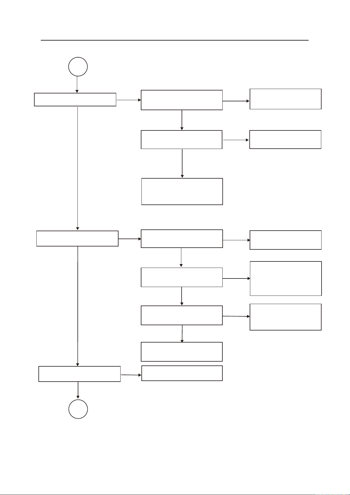
D
SERVICE MANUAL
Spindle revolves?
YES
Track on OK?
NO
NO
MT1369's DMSO outputs
normally?
YES
Check the signals SP+ and
SP- for normality.
YES
Check the circuit between the
spindle and BA5954.
MT1336 outputs correct TEO
signal?
YES
MT1339 outputs correct TRSO
signal?
NO
NO
NO
NO
Check MT1369 and its
peripheral circuit.
Check BA5954 and its
peripheral circuit.
Check the peripheral
circuit of MT1336.
Check the circuit between
MT1369 and BA5954's
TRSO signal.
YES
YES
The signals T+ and T- output
normally?
NO
Check the peripheral
circuit of BA5954.
YES
Check the circuits between
T+/T- and laser head.
Disk is ready?
NO
Check RF signal.
YES
E
75
Page 76
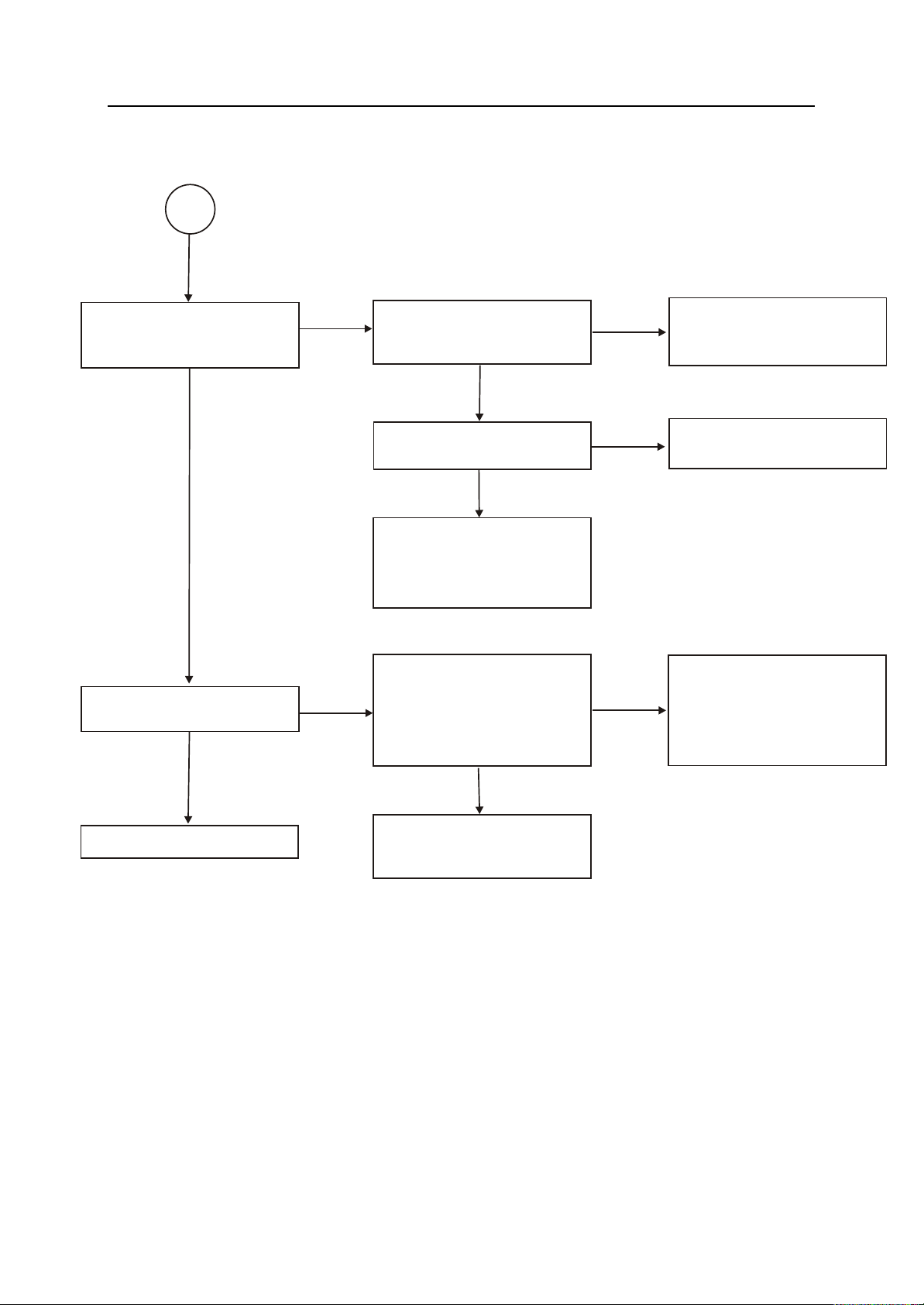
E
SERVICE MANUAL
Check audio output for
normality during playback.
YES
The IR, VFD and control
buttons work normally?
NO
NO
Check if data received
by AUDIO DAC for
Correctness.
YES
AUDIO DAC outputs
correctly?
YES
Check connections to
audio filter, audio
amplifier, mute and
output.
Check communication
between the
IR/VFD/control buttons
and MT1369 for
normality.
NO
NO
NO
Check MT1369 and the
circuit between it and
AUDIO DAC.
Check the peripheral
circuit of AUDIO DAC.
Check connection
between MT1369 and
module, and the
peripheral circuit of IR,
VFD and drive IC.
YES
YES
Debugging completed.
76
Check connections to
the remote control,
button matrix and VFD.
Page 77
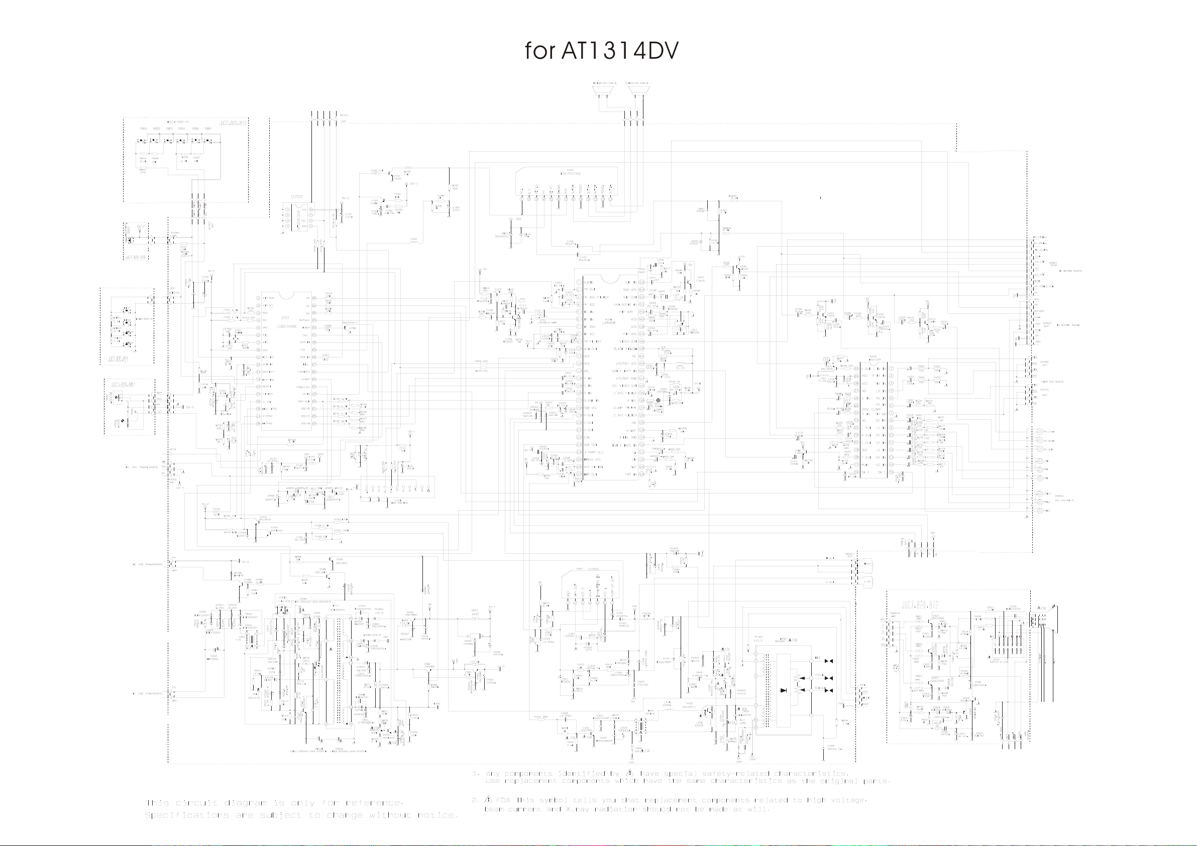
Circuit Diagram for AT1314DV
Page 78
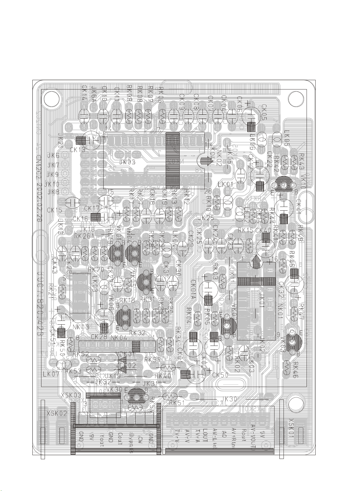
N-COMB PCB ASSEMBLY
Page 79
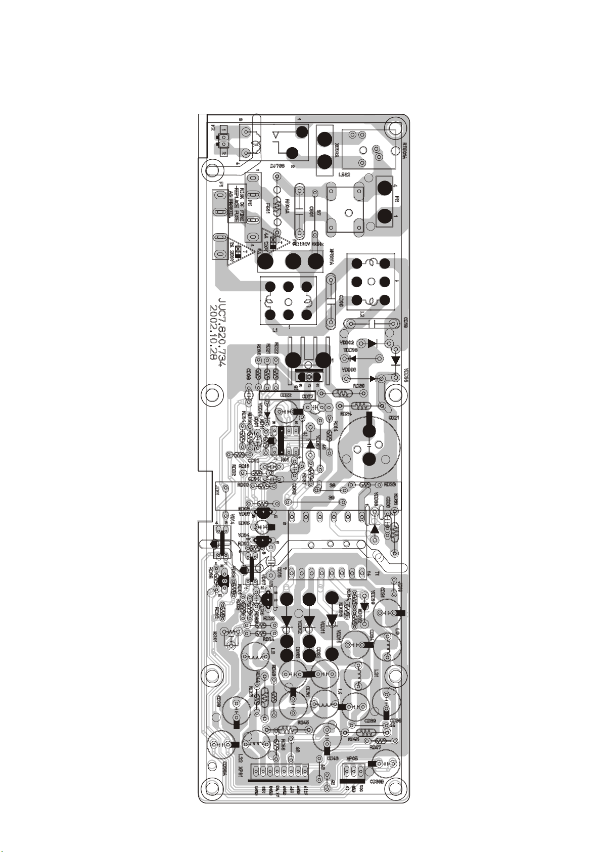
DVD Power PCB
Page 80
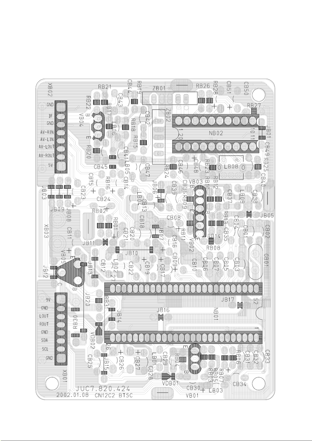
BTSC PCB
Page 81
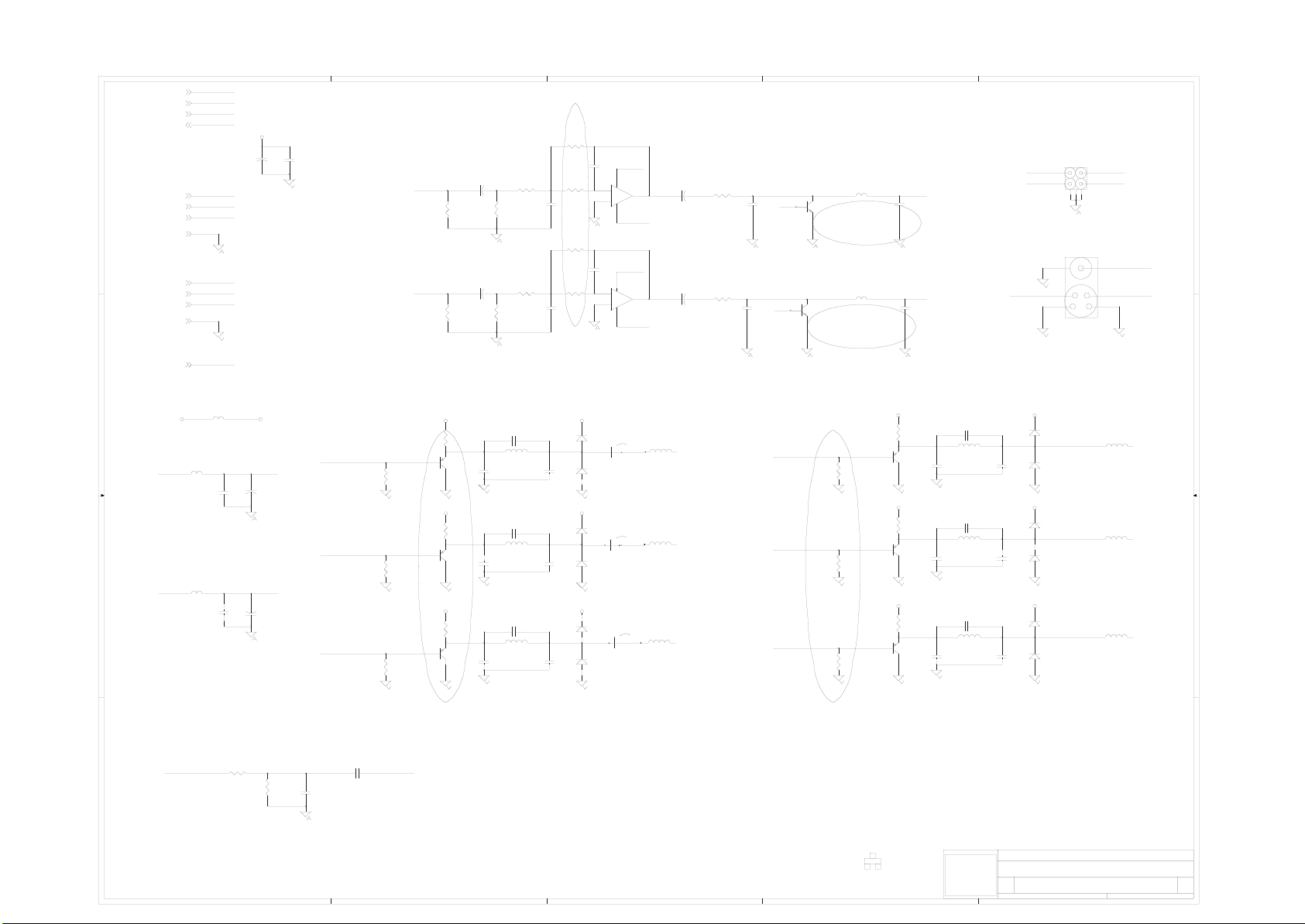
Circuit Diagram for DVD130A (1)
[ 1,2,3,4 ][ 1,2,3,4 ]
[ 1 ][ 1 ]
[ 1 ][ 1 ]
[ 4 ][ 4 ]
DD
CC
BB
[ 1,2,3,4 ][ 1,2,3,4 ]
[ 1,2,3,4 ][ 1,2,3,4 ]
[ 4 ][ 4 ]
[ 4 ][ 4 ]
[ 4 ][ 4 ]
[ 4 ][ 4 ]
[ 4 ][ 4 ]
[ 2 ][ 2 ]
+P12V+P12V
A_MUTEA_MUTE
T_CVBST_CVBS
ASPDIFASPDIF
-P12V-P12V
-P12V-P12V
-P12V-P12V
+P12V+P12V
+P12V+P12V
+12V+12V
+12V+12V
RMAINRMAIN
RMAINRMAIN[ 4 ][ 4 ]
LMAINLMAIN
LMAINLMAIN
A_MUTEA_MUTE
AGNDAGND
AGNDAGND
T_SYT_SY
T_SYT_SY
T_SCT_SC
T_SCT_SC
T_CVBST_CVBS
VGNDVGND
VGNDVGND
ASPDIFASPDIF
VCCVCC
33UH/030733UH/0307
L11L11
33UH/030733UH/0307
L13L13
33UH/030733UH/0307
+5VV+5VV
++
C83C83
CB92CB92
10u10u
0.1u0.1u
L14L14
CB81CB81 C73C73++
CB86CB86
0.1u0.1u
100uF/16V100uF/16V0.1u0.1u
C78C78
+5VV+5VV
+12V+12V
-12V-12V
++
100uF/16V100uF/16V
CVBS1CVBS1
Y/CVBS2Y/CVBS2
CHROMACHROMA
(9)(9)
R108R108
200200
R114R114
200200
R118R118
200200
55
VCCVCC
VCCVCC
44
LMAINLMAIN
267k267k 10k10k
RMAINRMAIN
R76R76
267k267k
+5VV+5VV
R105R105
75,1%75,1%
Q16Q16
39063906
+5VV+5VV
R111R111
75,1%75,1%
Q18Q18 1.8uH/08051.8uH/0805
39063906
+5VV+5VV
R116R116
75,1%75,1%
Q20Q20
39063906
33
(9)(9)
R64R64
18K18K
C74C74
-12V-12V
220p220p
(OPEN0(OPEN0
(OPEN0(OPEN0
R67R67
5.1k5.1k
C77C77
2000p2000p
R70R70
18K18K
R72R72
5.1k5.1k
C82C82
2000p2000p
C118C118
220P220P
C126C126
220P220P
C132C132
220P220P
C75C75
R66R66
++
10u10u
10k10k
R75R75R74R74
C80C80
R71R71
++
10u10u
10k10k
R77R77
10k10k
C114C114
10p10p
L16L16
1.8uH/08051.8uH/0805
C117C117
220p220p
C121C121
10p10p
L17L17
C125C125
220p220p
C128C128
(OPEN0(OPEN0
10p10p
L18L18
1.8uH/08051.8uH/0805
C131C131
220p220p
44
--
22
U9AU9A
++
33
NJM4580NJM4580
SSOP8SSOP8
88
+12V+12V
C79C79
-12V-12V
220p220p
44
--
66
U9BU9B
++
55
NJM4580NJM4580
SSOP8SSOP8
88
+12V+12V
+5VV+5VV
22
D3D3
C99C99
1N41481N4148
22 11
++
100U100U
D5D5
1N41481N4148
11
+5VV+5VV
D7D7
C97C97
1N41481N4148
++
100U100U
D9D9
1N41481N4148
11 22 11 22
+5VV+5VV
D11D11
C98C98
1N41481N4148
22 11 22
++
100U100U
D13D13
1N41481N4148
11
C76C76
R68R68
10u10u
100100
++
11
C81C81
10u10u
++
77
FB4FB4
HM102/0805HM102/0805
FB5FB5
HM102/0805HM102/0805
FB6FB6
HM102/0805HM102/0805
CB82CB82
A_MUTEA_MUTE
A_MUTEA_MUTE
R/CrR/Cr
G/YCVBS2G/YCVBS2
B/CbB/Cb
Q9Q9
39043904
Q10Q10
39043904
R87R87
200200
R90R90
200200
R92R92
200200
100P100P
R73R73
100100
CB87CB87
100P100P
22
RCHRCH
L12L12
33UH/030733UH/0307
L15L15
33UH/030733UH/0307
(9)(9)
LCHLCH
CB83CB83
100P100P
(8)(8)
RCHRCH
CB88CB88
100P100P
(8)(8)
+5VV+5VV
R88R88
75,1%75,1%
Q19Q19
39063906
+5VV+5VV
R89R89
75,1%75,1%
Q21Q21
39063906
+5VV+5VV
R91R91
75,1%75,1%
Q22Q22
39063906
C86C86
10p10p
L19L19
1.8uH,DIP1.8uH,DIP
C51C51
220p220p
C90C90
10p10p
L21L21
1.8uH,DIP1.8uH,DIP
C92C92
220p220p
C93C93
10p10p
L23L23
1.8uH,DIP1.8uH,DIP
C95C95
220p220p
LCHLCH
SCSC
+5VV+5VV
22
22 11
C89C89
220P220P
11
+5VV+5VV
C91C91
220P220P
11 1122 22
+5VV+5VV
1122 22
C94C94
220P220P
11
D4D4
1N41481N4148
D6D6
1N41481N4148
D10D10
1N41481N4148
D8D8
1N41481N4148
D14D14
1N41481N4148
D12D12
1N41481N4148
11
J2J2
AUDIOAUDIO
22
55
CVBSCVBS
44
66
CVBSCVBS
11
77
33
SPDIFSPDIF
J1J1
66
33
22
SPDIFOUTSPDIFOUT
55
SYSY
44
11
DD
S-videoS-video
CC
R/Cr-OUTR/Cr-OUT
FB1FB1
HM102/0805HM102/0805
G/Y/CVBS2-OUTG/Y/CVBS2-OUT
FB2FB2
HM102/0805HM102/0805
BB
B/Cb-OUTB/Cb-OUT
FB3FB3
HM102/0805HM102/0805
ASPDIFASPDIF
AA
R107R107
R109R109100100
100100
SPDIF Interface ( Coaxial )SPDIF Interface ( Coaxial )
55
CB106CB106
SPDIFOUTSPDIFOUT
0.1u0.1u
C119C119
330p330p
39063906
CC
BB
EE
44
33
22
MediaTek IncorporationMediaTek Incorporation
TitleTitle
DVD130(MT1369AE)DVD130(MT1369AE)
Document NumberDocument Number
SizeSize
CC
Wednesday, July 24, 2002Wednesday, July 24, 2002
Date:Date:
AV OUTPUTAV OUTPUT
11
SheetSheet 55
ofof 55
AA
RevRev
22
Page 82
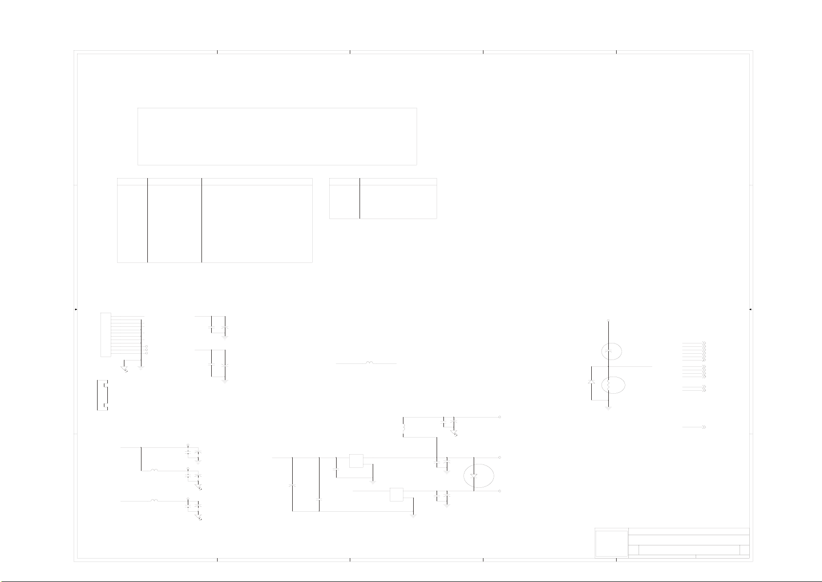
Circuit Diagram for DVD130A (2)
55
44 33
22 11
3-SY3669P2-V23-SY3669P2-V2
MT1369E (LQFP208) DVD MP Board for Sanyo SF-HD6AV PUHMT1369E (LQFP208) DVD MP Board for Sanyo SF-HD6AV PUH
DD
NAMENAME
VCCVCC
RVCCRVCC
AVCCAVCC
V33V33
DV33DV33
V25V25
+5VA+5VA
JP7JP7
CON12CON12
||
VV
+3VV+3VV
+5VV+5VV
+12V+12V
+P12V+P12V
11
22
PGNDPGND
-P12V-P12V
33
44
+P5V+P5V
55
PGNDPGND
+P3.6V+P3.6V
66
77
PGNDPGND
+PS5V+PS5V
88
99
GNDGND
-P22V-P22V
1010
AC35V+AC35V +
1111
AC35V-AC35V-
1212
SGNDSGND
11
CC
+12V+12V
GNDGND
-12V-12V
D5VD5V
GNDGND
3.6V3.6V
GNDGND
S5VS5V
GNDGND
-22V-22V
~3.5V~3.5V
~3.5V~3.5V
BB
1 INDEX & POWER, RESET1 INDEX & POWER, RESET
2 RF / SERVO & MPEG - MT1336E / MT1369E2 RF / SERVO & MPEG - MT1336E / MT1369E
3 MEMORY - SDRAM, FLASH/EEPROM3 MEMORY - SDRAM, FLASH/EEPROM
4 AUDIO - CS4334, VIDEO - CS4954/554 AUDIO - CS4334, VIDEO - CS4954/55
5 AV FILTER.5 AV FILTER.
TYPETYPE
Digital 5VDigital 5V
Servo 5VServo 5V
RF 5VRF 5V
Digital 3.3VDigital 3.3V
Digital 3.3VDigital 3.3V
Digital 2.5VDigital 2.5V
Audio 5VAudio 5V
Video 3.3VVideo 3.3V
Video 5VVideo 5V
Audio 12VAudio 12V
-P22V-P22V
AC35V+AC35V +
AC35V-AC35V-
DEVICEDEVICE
SUPPLYSUPPLY
MT1336EMT1336E
PICKUP HEADERPICKUP HEADER
SDRAM, Flash, VideoDACSDRAM, Flash, VideoDAC
MT1369EMT1369E
MT1369EMT1369EAV33AV33 Servo 3.3VServo 3.3V
MT1369EMT1369E
Audio DACAudio DAC
Video DACVideo DAC
Video DACVideo DAC
Audio filterAudio filter
+P12V+P12V
CB60CB60
++
0.1u0.1u
-P12V-P12V
CB62CB62
0.1u0.1u
++
C59C59
220u220u
C61C61
220u220u
NAMENAME
GNDGND
AGNDAGND
VGNDVGND
DD
TYPETYPE
Digital GroundDigital Ground
Servo Analog GroundServo Analog GroundSGNDSGND
Audio GroundAudio Ground
Video GroundVideo Ground
CC
V33V33
+P5V+P5V
+P5V+P5V
+P12V+P12V
++C58C58
(11)(11)
L20L20
+P36V+P36V
33UH/030733UH/0307
DV33DV33
D1D1
RLS4148ERLS4148E
10u10u
URSTURST
R50R50
(11)(11)
4.7k4.7k
-P12V-P12V
VCCVCC
RVCCRVCC
AVCCAVCC
DV33DV33
V33V33
AV33AV33
V25V25
GNDGND
SGNDSGND
[ 2,3,4,5 ][ 2,3,4,5 ]
+P12V+P12V
[ 5 ][ 5 ]
-P12V-P12V
[ 5 ][ 5 ]
VCCVCC
[ 2,3,4,5 ][ 2,3,4,5 ]
RVCCRVCC
[ 2 ][ 2 ]
AVCCAVCC
[ 2 ][ 2 ]
DV33DV33
[ 2,3,4 ][ 2,3,4 ]
V33V33
[ 2,3,4 ][ 2,3,4 ]
[ 2 ][ 2 ]
[ 2 ][ 2 ]
[ 2,3,4,5 ][ 2,3,4,5 ]
[ 2,3,4,5 ][ 2,3,4,5 ]
BB
AV33AV33
V25V25
GNDGND
SGNDSGND
Pitch=2.54 m/mPitch=2.54 m/m
+P5V+P5V
L8L8
33UH/030733UH/0307
AA
L7L7
+PS5V+PS5V
33UH/030733UH/0307
55
VCCVCC
VCCVCC
AVCCAVCC
RVCCRVCC
++
C64C64
CB65CB65
100U100U
0.1u0.1u
AVCCAVCC
++
C67C67
CB69CB69
100U100U
0.1u0.1u
RVCCRVCC
++
C66C66
CB68CB68
100U100U
0.1u0.1u
+P5V+P5V
C63C63
++
100u100u
CB67CB67
0.1u0.1u
44
SOT223SOT223
U11U11
G960T63UG 960T63U
33
22
VOVO
VIVI
11
+P36V+P36V
GNDGND
SOT223SOT223
U12U12
G950T63UG 950T63U
33
VIVI VOVO
GNDGND
CB64CB64
0.1u0.1u
L6L6 0.1u0.1u
33UH/030733UH/0307
22
11
33
CB61CB61
V33V33
++
CB63CB63
0.1u0.1u
CB66CB66
0.1u0.1u
C62C62
220u220u
++
C65C65
100u100u
AV33AV33
++
C60C60
220u220u
AV33AV33
DV33DV33
DV33DV33
(6)(6)
D2D2
1N40011N4001
(OPEN)(OPEN)
V25V25
V25V25
MediaTek IncorporationMediaTek Incorporation
TitleTitle
DVD130(MT1369AE)DVD130(MT1369AE)
Document NumberDocument Number
SizeSize
CC
Wednesday, July 24, 2002Wednesday, July 24, 2002
22
Date:Date:
URSTURST
Index & POWER Index & POWER
11
SheetSheet 11
URSTURSTAA[ 2 ][ 2 ]
ofof 55
RevRev
22
Page 83
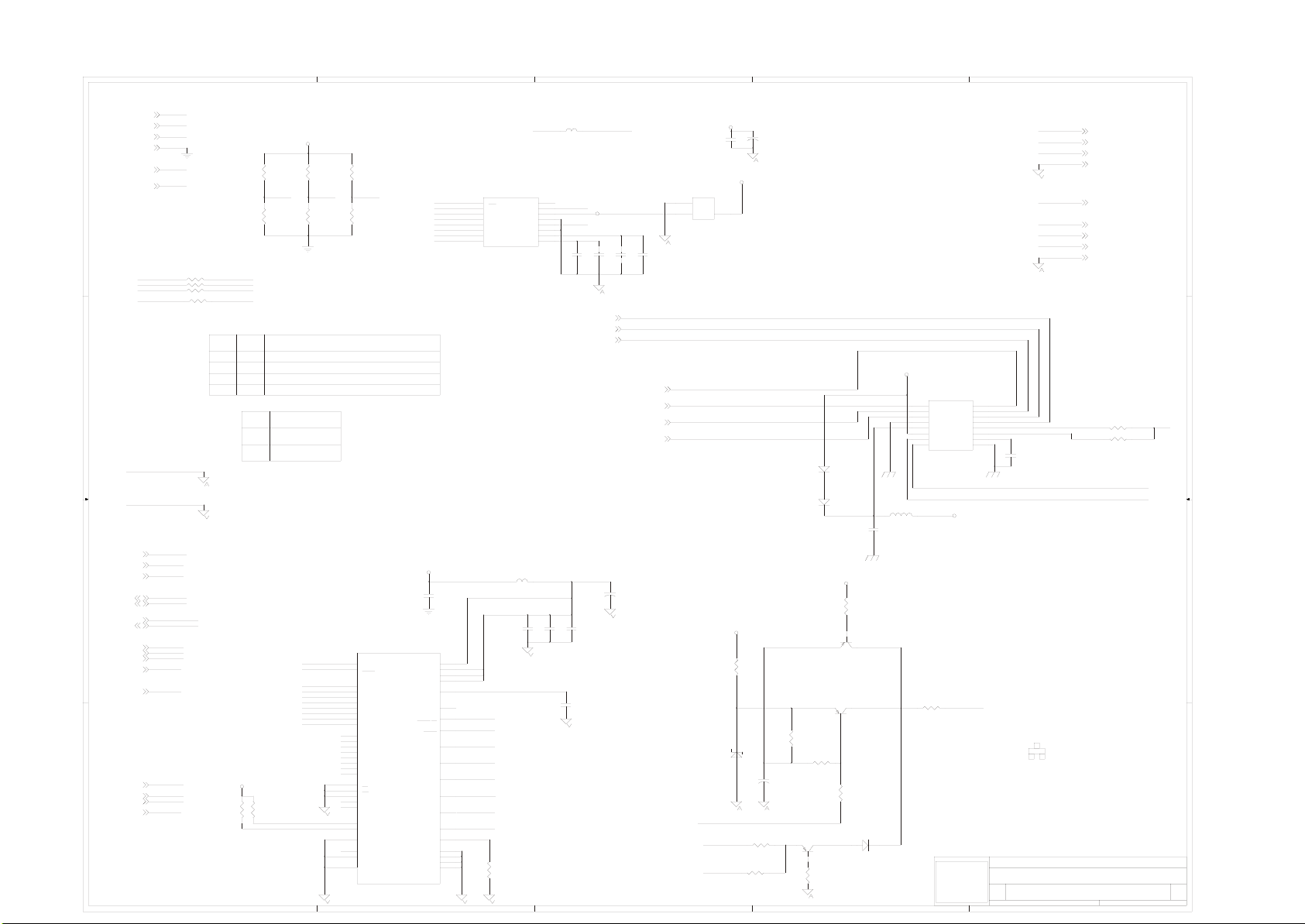
Circuit Diagram for DVD130A (3)
55
[ 1,5 ][ 1,5 ]
[ 5 ][ 5 ] +12V+12V
VCCVCC
VCCVCC
DV33DV33
DV33DV33
+P5V+P5V
+P5V+P5V
GNDGND
+P12V+P12V
+P12V+P12V
+12V+12V
SACLKSACLK
3333
SLRCKSLRCK
3333
SBCLKSBCLK
3333
SDAT0SDAT0
3333
ASDAT0ASDAT0
ALRCKALRCK
ABCKABCK
ACLKACLK
R53R53
R85R85
R84R84
R86R86
DIF1DIF100DIF0DIF0
00
00
11
11
00
11
11
DEM0DEM0
VCCVCC
R82AR82AR80AR80A
00
00
NO STUFFNO STUFF
DIF1DIF1
DIF0DIF0
R83AR83A
R81AR81A
00
00
NO STUFFNO STUFF
DescriptionsDescriptions
I2S , Up to 24-bitI2S , Up to 24-bit
Left Justified, Up to 24-bitLeft Justified, Up to 24-bit
Right Justified, 24-bitRight Justified, 24-bit
Right Justified, 16-bitRight Justified, 16-bit
DescriptionDescription
R84AR84A
00
DEM0DEM0
R85AR85A
00
NO STUFFNO STUFF
[ 1,2,3,5 ][ 1,2,3,5 ]
[ 1,2,3 ][ 1,2,3 ]
[ 1,2,3,5 ][ 1,2,3,5 ]
[ 1,2,3,5 ][ 1,2,3,5 ] GNDGND
DD
CC
00 DisableDisable
11 44.1 KHz44.1 KHz
AGNDAGND
GNDGND
VGNDVGND
GNDGND
RST_TVERST_TVE
RST_TVERST_TVE
MUTE#MUTE#
[ 2 ][ 2 ]
MUTE#MUTE#
RESET#RESET#
[ 2 ][ 2 ]
RESET#RESET#
SCLSCL
SDASDA
[ 2 ][ 2 ]
VSCKVSCK
VSDAVSDA
[ 2 ][ 2 ]
ACLKACLK
[ 2 ][ 2 ]
ABCKABCK
[ 2 ][ 2 ]
ALRCKALRCK
[ 2 ][ 2 ] ASDAT0ASDAT0
ASPDIFASPDIF
[ 2 ][ 2 ]
27MHZ27MHZ
[ 2 ][ 2 ]
HSYNC#HSYNC #
[ 2 ][ 2 ]
VSYNC#VSYNC#
[ 2 ][ 2 ]
Y[0..7]Y[0..7]
SCLSCL
SDASDA
VSCKVSCK
VSDAVSDA
ACLKACLK
ABCKABCK
ALRCKALRCK
ASDAT0ASDAT0
ASPDIFASPDIF
27MHZ27MHZ
HSYNC#HSYNC #
VSYNC#VSYNC#
Y[0..7]Y[0..7]
2929
3434
11
22
33
44
55
66
77
88
2626
2525
2424
2323
2222
2121
2020
1919
2727
2828
3030
3131
1212
3232
3333
1313
1414
1515
1616
CS4954, TQFP-48CS4954, TQFP-48
U14U14
CLOCKCLOCK
RESETRESET
V0V0
V1V1
V2V2
V3V3
V4V4
V5V5
V6V6
V7V7
PDAT0PDAT0
PDAT1PDAT1
PDAT2PDAT2
PDAT3PDAT3
PDAT4PDAT4
PDAT5PDAT5
PDAT6PDAT6
PDAT7PDAT7
RDRD
WRWR
TTXDATTTXDAT
TTXRQTTXRQ
INTINT
SDASDA
SCLSCL
TESTTEST
XTALOUTXTALOUT
XTALINXTALIN
PADDRPADDR
27MHZ27MHZ
RST_TVERST_TVE
Y0Y0
Y1Y1
Y2Y2
Y3Y3
Y4Y4
Y5Y5
Y6Y6
Y7Y7
VCCVCC
R52R52R51R51
680680
680680
55
SDASDA
SCLSCL
[ 2,3 ][ 2,3 ]
BB
[ 2,3 ][ 2,3 ]
[ 2 ][ 2 ]
[ 2,5 ][ 2,5 ]
AA
44
L9L9
VCCVCC +5VA+5VA
33UH/LA030733UH/LA0307
U13U13
RESET#RESET#
11
RSTRST
SDAT0SDAT0
SDATASDATA
SBCLKSBCLK
33
SCLK/DEM1SCLK/DEM1
SLRCKSLRCK
44
LRCKLRCK
SACLKSACLK
55
MCLKMCLK
DIF1DIF1
66
DIF1DIF1
DIF0DIF0
77
DIF0DIF0
DEM0DEM0
88
DEM0DEM0
CS4340CS4340
DV33DV33
CB74CB74
0.1u0.1u
1717
VDDVDD
3636
VAAVAA
4141
VAAVAA
4646
VAAVAA
3838
VREFVREF
99
FIELD/CBFIELD/CB
HSYNC#HSYNC#
1010
HSYNC/CBHSYNC/CB
VSYNC#VSYNC#
1111
VSYNCVSYNC
CVBSCVBS
REDRED
GREENGREEN
BLUEBLUE
ISETISET
GNDDGNDD
GNDAGNDA
GNDAGNDA
GNDAGNDA
44 33
CVBS1CVBS1
4444
Y/CVBS2Y/CVBS2
4848
YY
CC
CC
4747
R/CrR/Cr
3939
G/Y/CVBS2G/Y/CVBS2
4040
B/CbB/Cb
4343
3737
1818
3535
4242
4545
R62R62
4k, 1%4k, 1%
MUTECMUTEC
AOUTLAOUTL
AOUTRAOUTR
REF_GNDREF_GND
FILT+FILT+
L10L10
33UH/030733UH/0307
1616
LMAINLMAIN151522
1414
VccVcc
1313
GNDGND
1212
1111
1010
VQVQ
99
CB75CB75
0.1u0.1u
RMAINRMAIN
CB76CB76 CB77CB77
0.1u0.1u
CB71CB71 C69C69
0.1u0.1u
VSDA(U3.61)VSDA(U3.61)
UP3..0(U3.66)UP3..0(U3.66)
UP1..5(U3.62)UP1..5(U3.62)
0.1u0.1u
CB80CB80
0.1u0.1u
+5VA+5VA
1u1u
C72C72++
47u47u
33
+5VA+5VA
CB70CB70 C68C68
0.1u0.1u
1u1u
+12V+12V
U15U15
11
GNDGND
22
33
VOVO
VIVI
7805_27805_2
C70C70CB73CB73
1u1u
0.1u0.1u
MCLKMCLK
TBCK--TBCK--
TSD0--TSD0--
TWSTWS
ZD1ZD1
Zener / 5V1Zener / 5V1
MUTE#MUTE#
BCKBCK
LRCKLRCK
MUTECMUTEC
ZEROZERO
DATADATA
+12V+12V
R54R54
470/0.25W470/0.25W
DIP, pitch=10m/mDIP, pitch=10m/m
R57R57
7.5k7.5k
C71C71
++
100u/25V100u/25V
R93R93
R99R99
4.7K4.7K
Q24Q24
39063906
1K1K
22
VCCAVCCA
2-CHANNEL,AUDIODAC2-CHANNEL,AUDIODAC
U19U19
11
22
33
44
55
66
77
88
D18D18
RLS4148RLS4148
D17D17
RLS4148RLS4148
Q8Q8
39063906
R58R58
22k22k
R94R94
1K1K
+5VA+5VA
Q7Q7
39063906
1N40011N4001
3.3UH/08053.3UH/0805
L22L22
CB48CB48
0.1UF0.1UF
R55R55
10k10k
R56R56
8282
R99R99
4.7K4.7K
D16D16
22
BCKBCK
DATADATA
LRCKLRCK
DGNDDGND
VDDVDD
VCCVCC
VORVOR AGNDAGND
PCM1748EPCM1748E
VCC33VCC33
VcomVcomVOLVOL
SCKSCK
MLML
MCMC
MDMD
ZLZL
ZRZR
A_MUTEA_MUTE
1616
1515
1414
1313
1212
1111
1010
99
TitleTitle
DVD130(MT1369AE)
Document NumberDocument Number
SizeSize
CC
Date:Date:
++
C96C96
47uF47uF
BB
39063906
MediaTek IncorporationMediaTek Incorporation
Wednesday, July 24, 2002Wednesday, July 24, 2002
ASPDIFASPDIF
CC
EE
Audio & Video DACAudio & Video DAC
T_SYT_SY
T_SCT_SC
T_CVBST_CVBS
VGNDVGND
RMAINRMAIN
LMAINLMAIN
A_MUTEA_MUTE
AGNDAGND
ZLZL
ZRZR
11
T_SYT_SY
T_SCT_SC
T_CVBST_CVBS
VGNDVGND
ASPDIFASPDIF [ 2,5 ][ 2,5 ]
RMAINRMAIN
LMAINLMAIN
AGNDAGND [ 1,2,3,5 ][ 1,2,3,5 ]
R97R97 10k10k
R98R98
10k10k
SheetSheet 44 ofof 55
11
[ 5 ][ 5 ]
[ 5 ][ 5 ]
[ 5 ][ 5 ]
[ 1,2,3,5 ][ 1,2,3,5 ]
[ 5 ][ 5 ]
[ 5 ][ 5 ]
[ 5 ][ 5 ]A_MUTEA_MUTE
DD
CC
ZEROZERO
VORVOR
VOLVOL
BB
AA
RevRev
22
Page 84
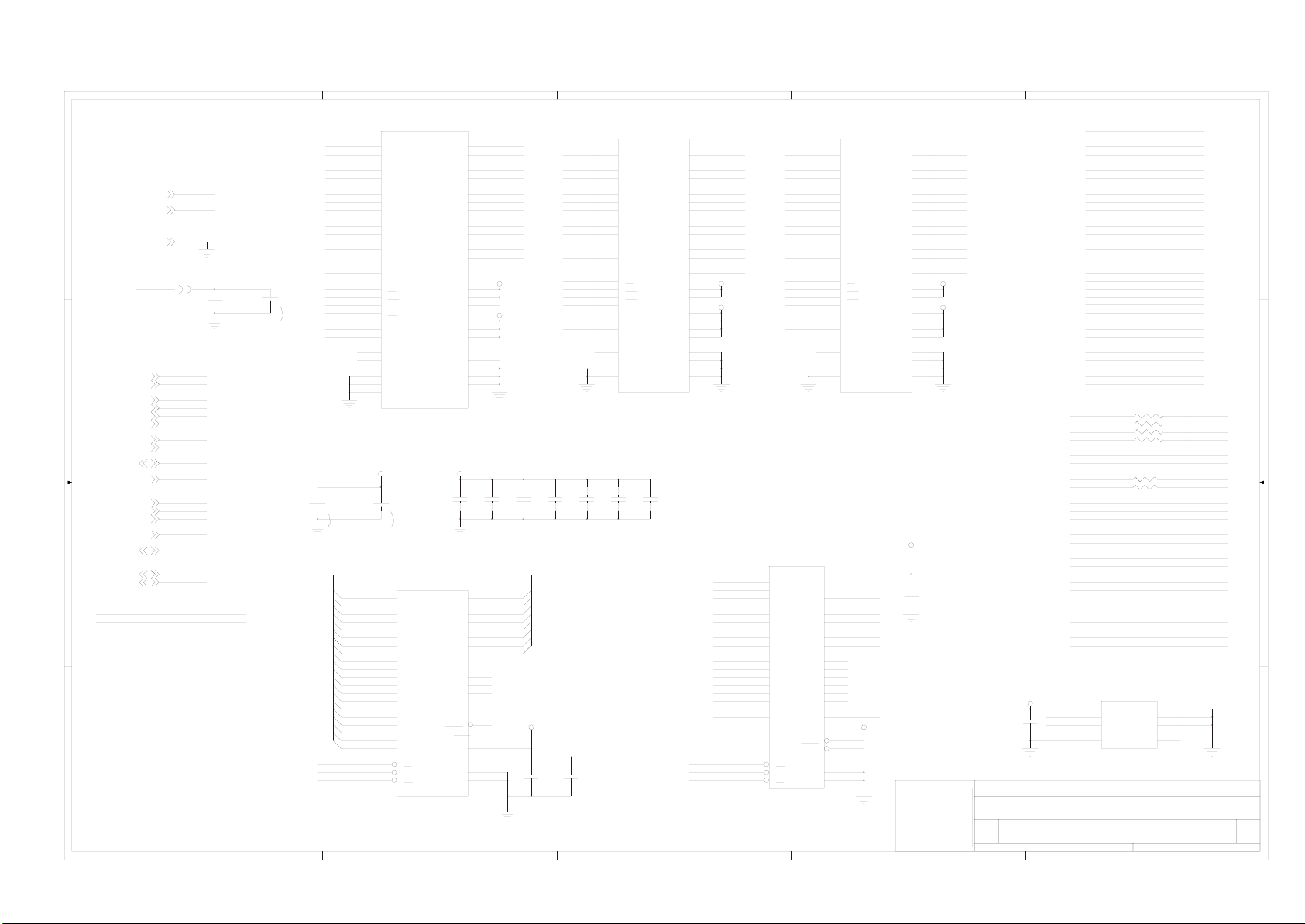
Circuit Diagram for DVD130A (4)
55
U6U6
DMA0DMA0
2323
2424
2525
2626
2929
3030
3131
3232
3333
3434
2222
3535
2020
2121
3838
3737
1919
1818
1717
1616
1515
3939
3636
4040
5454
4141
2828
SD33SD33
A0A0
A1A1
A2A2
A3A3
A4A4
A5A5
A6A6
A7A7
A8A8
A9A9
A10A10
A11A11
A12A12
A13A13
A14A14
A15A15
A16A16
A17A17
A18A18
A19A19
A0A0
A1A1
A2A2
A3A3
A4A4
A5A5
A6A6
A7A7
A8A8
A9A9
A10/APA10/AP
A11A11
BA0/A13BA0/A13
BA1/A12BA1/A12
CLKCLK
CKECKE
CSCS VCCVCC
RASRAS
CASCAS
WEWE
DQMLDQML
DQMHDQMH
NCNC
NCNC
VSSVSS
VSSVSS
VSSVSS
SDRAM 1Mx16x4SDRAM 1Mx16x4
EliteMT M12L64164A-5TEliteMT M12L64164A-5T
54-Pin TSOPII(400mil x 875mil)54-Pin TSOPII(400mil x 875mil)
++
2121
2020
1919
1818
1717
1616
1515
1414
88
77
3636
66
55
44
33
22
11
4040
1313
3737
2222
2424
99
DMA1DMA1
DMA2DMA2
DMA3DMA3
DMA4DMA4
DMA5DMA5
A[0..19]A[0..19]
DMA6DMA6
DMA7DMA7
DMA8DMA8
DMA9DMA9
DMA10DMA10
DMA11DMA11
DBA0DBA0
DBA1DBA1
SDCLKSDCLK
SDCKESDCKE
DCS#DCS#
DRAS#DRAS#
DCAS#DCAS#
DWE#DWE#
RDQM0RDQM0
RDQM1RDQM1
C56C56
++
47u47u
FCE#FCE#
FRD#FRD#
FWR#FWR#
VCCVCC
V33V33[ 1,2,4 ][ 1,2,4 ]
GNDGND
VCCVCC
V33V33
GNDGND
L5L5
V33V33
FB / 0805FB / 0805
DCLKDCLK
DCKEDCKE
CAS#CAS#
RAS#RAS#
WE#WE#
CS#C S#
MA[0..11]MA[0..11]
BA[0..1]BA[0..1]
CB49CB49
0.1u0.1u
SD33SD33
C55C55++
47u47u
DQ[0..31]DQ[0..31]
DQM[0..3]DQM[0..3]
PCE#PCE#
PRD#PRD#
PWR#PWR#
A[0..19]A[0..19]
AD[0..7]AD[0..7]
SCLSC L
SDASDA
FCE#FCE#
FRD#FRD#
FWR#FWR#
55
[ 1,2,4,5 ][ 1,2,4,5 ]
DD
[ 1,2,4,5 ][ 1,2,4,5 ]
[ 2 ][ 2 ]
DCLKDCLK
[ 2 ][ 2 ]
CC
BB
AA
DCKEDCKE
[ 2 ][ 2 ]
CAS#CAS#
[ 2 ][ 2 ]
RAS#RAS#
[ 2 ][ 2 ]
WE#WE#
[ 2 ][ 2 ]
CS#C S#
[ 2 ][ 2 ]
MA[0..11]MA[0..11]
[ 2 ][ 2 ]
BA[0..1]BA[0..1]
[ 2 ][ 2 ]
DQ[0..31]DQ[0..31]
[ 2 ][ 2 ]
DQM[0..3]DQM[0..3]
[ 2 ][ 2 ]
PCE#PCE#
[ 2 ][ 2 ]
PRD#PRD#
[ 2 ][ 2 ]
PWR#PWR#
[ 2 ][ 2 ]
A[0..19]A[0..19]
[ 2 ][ 2 ]
AD[0..7]AD[0..7]
[ 2,4 ][ 2,4 ]
SCLSC L
[ 2,4 ][ 2,4 ]
SDASDA
PCE#PCE#
PRD#PRD#
PWR#PWR#
44
C57C57
47u47u
U8U8
A0A0
A1A1
A2A2
A4A4
A5A5
A6A6
A7A7
A8A8
A9A9
A10A10 NCNC
A11A11
A12A12
A13A13
A14A14
A15A15
A16A16
A18A18
A19A19
CECE
OEOE
WEWE
Flash 8M, SST-40TSOPFlash 8M, SST-40TSOP
44
DQ0DQ0
DQ1DQ1
DQ2DQ2
DQ3DQ3
DQ4DQ4
DQ5DQ5
DQ6DQ6
DQ7DQ7
DQ8DQ8
DQ9DQ9
DQ10DQ10
DQ11DQ11
DQ12DQ12
DQ13DQ13
DQ14DQ14
DQ15DQ15
VCCVCC
VCCVCC
VCCQVCCQ
VCCQVCCQ
VCCQVCCQ
VCCQVCCQ
VSSQVSSQ
VSSQVSSQ
VSSQVSSQ
VSSQVSSQ
RESETRESET
RY/BYRY/RY/BYRY/A17A17
VCCVCC
VCCVCC
VSSVSS
VSSVSS
SD33SD33
33
22
RDQ0RDQ0
44
RDQ1RDQ1
55
RDQ2RDQ2
77
RDQ3RDQ3
88
RDQ4RDQ4
1010
RDQ5RDQ5
1111
RDQ6RDQ6
1313
RDQ7RDQ7
4242
RDQ8RDQ8
4444
RDQ9RDQ9
4545
RDQ10RDQ10
4747
RDQ11RDQ11
4848
RDQ12RDQ12
5050
RDQ13RDQ13
5151
RDQ14RDQ14
5353
RDQ15RDQ15
SD33SD33
11
1414
2727
SD33SD33
33
99
4343
4949
66
1212
4646
5252
DMA0DMA0
DMA1DMA1
DMA2DMA2
DMA3DMA3
DMA4DMA4
DMA5DMA5
DMA6DMA6
DMA7DMA7
DMA8DMA8
DMA9DMA9
DMA10DMA10
DBA0DBA0
SDCLKSDCLK
SDCKESDCKE 3434
DCS#DCS#
DRAS#DRAS#
DCAS#DCAS#
DWE#DWE#
RDQM0RDQM0
RDQM1RDQM1
U16U16
2121
A0A0
2222
A1A1
2323
A2A2
2424
A3A3 DQ3DQ3
2727
A4A4
2828
A5A5
2929
A6A6
3030
A7A7
3131
A8A8
3232
A9A9
2020
1919
BA/A11BA/A11
3535
CLKCLK
CKECKE
1818
CSCS
1717
RASRAS VCCVCC
1616
CASCAS
1515
WEWE
1414
DQMLDQML
3636
DQMHDQMH
3333
NCNC
3737
NCNC
2626
VSSVSS
5050
VSSVSS
DQ0DQ0
DQ1DQ1
DQ2DQ2
DQ4DQ4
DQ5DQ5
DQ6DQ6
DQ7DQ7
DQ8DQ8
DQ9DQ9
DQ10DQ10A10A10
DQ11DQ11
DQ12DQ12
DQ13DQ13
DQ14DQ14
DQ15DQ15
VCCVCC
VCCQVCCQ
VCCQVCCQ
VCCQVCCQ
VCCQVCCQ
VSSQVSSQ
VSSQVSSQ
VSSQVSSQ
VSSQVSSQ
22
33
55
66
88
99
1111
1212
3939
4040
4242
4343
4545
4646
4848
4949
11
2525
77
1313
3838
4444
44
1010
4141
4747
RDQ0RDQ0
RDQ1RDQ1
RDQ2RDQ2
RDQ3RDQ3 DMA3DMA3
RDQ4RDQ4
RDQ5RDQ5
RDQ6RDQ6
RDQ7RDQ7
RDQ8RDQ8
RDQ9RDQ9
RDQ10RDQ10
RDQ11RDQ11
RDQ12RDQ12
RDQ13RDQ13
RDQ14RDQ14
RDQ15RDQ15
SD33SD33
SD33SD33
DMA0DMA0
DMA1DMA1
DMA2DMA2
DMA4DMA4
DMA5DMA5
DMA6DMA6
DMA7DMA7
DMA8DMA8
DMA9DMA9
DMA10DMA10
DBA0DBA0
SDCLKSDCLK
SDCKESDCKE
DCS#DCS#
DRAS#DRAS#
DCAS#DCAS#
DWE#DWE#
RDQM2RDQM2
RDQM3RDQM3
SDRAM 512Kx16x2SDRAM 512Kx16x2
ESMT M12L16161A-5TESMT M12L16161A-5T
50-PIN TSOP(II),50-PIN TSOP(II),
(400milx825mil, 0.8mm pin pitch)(400milx825mil, 0.8mm pin pitch)
CB50CB50
CB51CB51
CB52CB52
CB53CB53
0.1u0.1u
0.1u0.1u 0.1u0.1u
CB54CB54
0.1u0.1u
0.1u0.1u
AD[0..7]AD[0..7]
2525
AD0AD 0
D0D0
2626
AD1AD 1
D1D1
2727
AD2AD 2
D2D2
2828
AD3AD 3
D3D3A3A3
3232
AD4AD 4
D4D4
3333
AD5AD 5
D5D5
3434
AD6AD 6
D6D6
3535
AD7AD 7
D7D7
1111
2929
NCNC
3838
NCNC
1010
1212
3030
3131
2323
3939
V33V33
CB78CB78
CB79CB79
0.1u0.1u
0.1u0.1u
CB56CB56CB55CB55
0.1u0.1u
0.1u0.1u
1111
1010
4242
4141
4040
3939
3838
3737
3636
3535
3434
4343
1414
1212
99
88
77
66
55
44
33
22
U7U7
A0A0
A1A1
A2A2
A3A3
A4A4
A5A5
A7A7
A8A8
A9A9
A10A10
A11A11
A12A12
A14A14
A15A15
A16A16
A17A17
A18A18
WEWE
OEOE
CECE
AT49F8192AAT49F8192A
8M Flash8M Flash
A0A0
A1A1
A2A2
A3A3
A4A4
A5A5
A6A6
A7A7
A8A8
A9A9
A10A10
A11A11
A12A12
A13A13
A14A14
A15A15
A16A16
A17A17
A18A18
FWR#FWR#
FRD#FRD#
FCE#FCE#
33
IO10IO10A13A13
IO11IO11
IO12IO12
IO13IO13
IO14IO14
IO15IO15
RESETRESET
BYTEBYTE
VccVcc
IO0IO0
IO1IO1
IO2IO2
IO3IO3A6A6
IO4IO4
IO5IO5
IO6IO6
IO7IO7
IO8IO8
IO9IO9
GNDGND
GNDGND
U17U17
2121
A0A0
2222
A1A1
2323
A2A2
2424
A3A3 DQ3DQ3
2727
A4A4
2828
A5A5
2929
A6A6
3030
A7A7
3131
A8A8
3232
A9A9
2020
1919
BA/A11BA/A11
3535
CLKCLK
3434
CKECKE
1818
CSCS
1717
RASRAS VCCVCC
1616
CASCAS
1515
WEWE
1414
DQMLDQML
3636
DQMHDQMH
3333
NCNC
3737
NCNC
2626
VSSVSS
5050
VSSVSS
SDRAM 512Kx16x2SDRAM 512Kx16x2
ESMT M12L16161A-5TESMT M12L16161A-5T
50-PIN TSOP(II),50-PIN TSOP(II),
(400milx825mil, 0.8mm pin pitch)(400milx825mil, 0.8mm pin pitch)
2323
1515
AD0AD 0
1717
AD1AD 1
1919
AD2AD 2
2121
AD3AD 3
2424
AD4AD 4
2626
AD5AD 5
2828
AD6AD 6
3030
AD7AD 7
1616
1818
2020
2222
2525
2727
2929
A19A19
3131
VCCVCC
4444
3333
1313
3232
DQ0DQ0
DQ1DQ1
DQ2DQ2
DQ4DQ4
DQ5DQ5
DQ6DQ6
DQ7DQ7
DQ8DQ8
DQ9DQ9
DQ10DQ10A10A10
DQ11DQ11
DQ12DQ12
DQ13DQ13
DQ14DQ14
DQ15DQ15
VCCVCC
VCCQVCCQ
VCCQVCCQ
VCCQVCCQ
VCCQVCCQ
VSSQVSSQ
VSSQVSSQ
VSSQVSSQ
VSSQVSSQ
22
DQ0DQ0
DQ1DQ1
CS#C S#
RAS#RAS#
CAS#CAS#
WE#WE#
BA0BA0
BA1BA1
DCLKDCLK
DCKEDCKE
MA0MA0
MA1MA1
MA2MA2
MA3MA3
MA4MA4
MA5MA5
MA6MA6
MA7MA7
MA8MA8
MA9MA9
MA10MA10
MA11MA11
DQM0DQM0
DQM1DQM1
DQM2DQM2
DQM3DQM3
DQ2DQ2
DQ3DQ3
DQ4DQ4
DQ5DQ5
DQ6DQ6
DQ7DQ7
DQ8DQ8
DQ9DQ9
DQ10DQ10
DQ11DQ11
DQ12DQ12
DQ13DQ13
DQ14DQ14
DQ15DQ15
DQ16DQ16
DQ17DQ17
DQ18DQ18
DQ19DQ19
DQ20DQ20
DQ21DQ21
DQ22DQ22
DQ23DQ23
DQ24DQ24
DQ25DQ25
DQ26DQ26
DQ27DQ27
DQ28DQ28
DQ29DQ29
DQ30DQ30
DQ31DQ31
RDQ16RDQ16
22
RDQ17RDQ17
33
RDQ18RDQ18
55
RDQ19RDQ19
66
RDQ20RDQ20
88
RDQ21RDQ21
99
RDQ22RDQ22
1111
RDQ23RDQ23
1212
RDQ24RDQ24
3939
RDQ25RDQ25
4040
RDQ26RDQ26
4242
RDQ27RDQ27
4343
RDQ28RDQ28
4545
RDQ29RDQ29
4646
RDQ30RDQ30
4848
RDQ31RDQ31
4949
SD33SD33
11
2525
SD33SD33
77
1313
3838
4444
44
1010
4141
4747
VCCVCC
CB57CB57
0.1u0.1u
V33V33
SDASDA
CB59CB59
0.1u0.1u
55
SCLSC L
66
11
33x433x4
RN1RN1
11
33
55
77
R47R47
R48R48
U10U10
NCNC
SDASDA
NCNC
SCLSCL
NCNC
WPWP
EEPROM 24C16, ST-SO8EEPROM 24C16, ST-SO8
M24C16-WM24C16-W
RDQ0RDQ0
RDQ1RDQ1
RDQ2RDQ2
RDQ3RDQ3
RDQ4RDQ4
RDQ5RDQ5
RDQ6RDQ6
RDQ7RDQ7
RDQ8RDQ8
RDQ9RDQ9
RDQ10RDQ10
RDQ11RDQ11
RDQ12RDQ12
RDQ13RDQ13
RDQ14RDQ14
RDQ15RDQ15
RDQ16RDQ16
RDQ17RDQ17
RDQ18RDQ18
RDQ19RDQ19
RDQ20RDQ20
RDQ21RDQ21
RDQ22RDQ22
RDQ23RDQ23
RDQ24RDQ24
RDQ25RDQ25
RDQ26RDQ26
RDQ27RDQ27
RDQ28RDQ28
RDQ29RDQ29
RDQ30RDQ30
RDQ31RDQ31
22
DCS#DCS#
DRAS#DRAS#
44
DCAS#DCAS#
66
88
DWE#DWE#
DBA0DBA0
DBA1DBA1
SDCLKSDCLK
3333
SDCKESDCKE
3333
DMA0DMA0
DMA1DMA1
DMA2DMA2
DMA3DMA3
DMA4DMA4
DMA5DMA5
DMA6DMA6
DMA7DMA7
DMA8DMA8
DMA9DMA9
DMA10DMA10
DMA11DMA11
RDQM0RDQM0
RDQM1RDQM1
RDQM2RDQM2
RDQM3RDQM3
11
22
33
77
DD
CC
BB
AA
MediaTek IncorporationMediaTek Incorporation
TitleTitle
izeSize
Document NumberDocument Number
FALSH & SDRAM & EEPROMFALSH & SDRAM & EEPROM
Wednesday, July 24, 2002Wednesday, July 24, 2002
SheetSheet
11
33 ofof 55
RevRev
22
Page 85
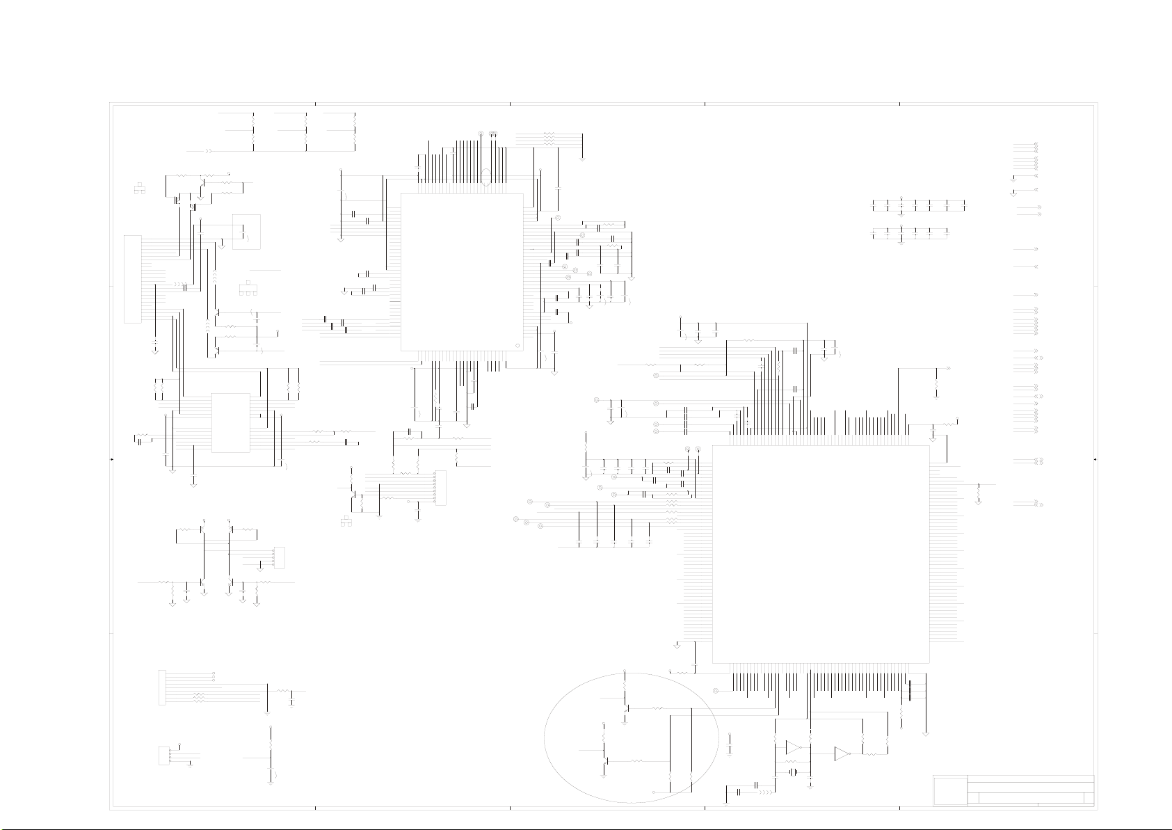
Circuit Diagram for DVD130A (5)
DD
CC
BB
AA
DD
33
22SS11
2SK30182SK3018
SF-HD6AV/0.5mm,24PSF-HD6AV/0.5mm,24P
TOP SIDE CONTACTEDTOP SIDE CONTACTED
GND-LDGND-LD
LD-DVDLD-DVD
HFMHFM
LD-CDLD-CD
MDMD
VR-DVDVR-DVD
VR-CDVR-CD
(LD-CD)(LD-CD)
NCNC
CD/DVDCD/DVD
CC
DD
FF
VCCVCC
VCVC
GND-PDGND-PD
EE
AA
BB
NCNC
T-T-
T+T+
F+F+
F-F-
CON1CON1
TROPENTROPEN
55
AVCCAVCC
LDO_AVCCLDO_AVCC
V33V33
L1L1
33UH/030733UH/0307
AVCCAVCC
R6R6
11
33
CB21CB21 0.1u0.1u
FMSOFMSO
TRSOTRSO
V1P4V1P4
STBYSTBY
R136R136
220220
R143R143
390390
-P22V-P22V
AC35V+AC35V+
AC35V-AC35V-
AGNDAGND
VSTBVSTB
VSCKVSCK
VSDAVSDA
V33V33
Q1Q1
2N39042N3904
11
33
33UH/030733UH/0307
C164C164
390P390P
RxDRxD
TxDTxD
10K10K
R7R7
R8R8
22
Q3Q3
2SK30182SK3018
AVCCAVCC
CB13CB13
0.1u0.1u
L2L2
33UH/030733UH/0307
Q4Q4
3CG8550D3CG8550D
L4L4
R11R11
R12R12
Q5Q5
3CG8550D3CG8550D
U2U2
1515
VOTK+VOTK+
1616
VOTK-VOTK-
1717
VOLD+VOLD+
1818
VOLD-VOLD-
1919 1010
PGNDPGND
2020
VNFTKVNFTK
2121
PVCC2PVCC2
2222
PREGNDPREGND
2323
VINLDVINLD
2424
CTK2CTK2
2525
CTK1CTK1
2626
VINTKVINTK
2727
BIASBIAS
2828
STBYSTBY
BA5954BA5954
CB41CB41
0.1u0.1u
VCCVCC
VCCVCC
Q12Q12
Q11Q11
85508550
TO-92TO-92
Q13Q13
80508050
-P22V-P22V
AC35V+AC35V+
AC35V-AC35V-
VFDVCCVFDVCC
R65R65
00
R69R69
00
R78R78
00
55
10K10K
100K100K
Very ImportantVery Important
to reduce Noiseto reduce Noise
BBEECC
2SB11322SB1132
2222
2222
VOFC+VOFC+
VOFC-VOFC-
VOSL+VOSL+
VOSL-VOSL-
PGNDPGND
PVCC1PVCC1
VNFFCVNFFC
VOSLVOSL
VINSL-VINSL-
VINSL+VINSL+
VINFCVINFC
GNDGND
V-STBV-STB
V-SCKV-SCK
V-SDAV-SDA
IOAIOA
++
CC
VCCVCC
CF2CF2
CF1CF1
R137R137
220220
LOAD-LOAD-
LOAD+LOAD+
TROUTTROUT
TRINTRIN
C165C165
390P390P
R5R5 100K100K
22
GG
Q2Q2
2SK30182SK3018
2424
2323
2222
2121
MDI1MDI1
2020
1919
1818
1717
1616
IOAIOA
1515
CC
1414
DD
1313
FF
1212
1111
L3L3
V20V20
1010
33UH/030733UH/0307
99
EE
88
AA
77
BB
66
55
44
33
22
11
CB31CB31
0.1u0.1u
R17R17
R18R18
1,08051,0805
1,08051,0805
SL+SL+
SL-SL-
VCCVCC
20k20kR25R25
C33C33
150p150p
CB39CB39
0.1u0.1u
R140R140
1K1K
JP6JP6
11
22
33
44
55
66
77
88
99
VFD, 2.0 m/mVFD, 2.0 m/m
JP8JP8
11
22
33
44
RS232/4P,2.0 m/mRS232/4P,2.0 m/m
RVCCRVCC
R61R61
00
RVCCINRVCCIN
R63R63
00
C3C3
100u100u
MDI1MDI1
MDI2MDI2
LDO2LDO2
C12C12
++
47u47u
LDO_AVCCLDO_AVCC
C18C18
++
47u47u
LDO1LDO1
R19R19
1,08051,0805
1414
1313
SP-SP-
1212
SP+SP+
1111
99
VCCVCC
88
77
66
55
V1P4V1P4
44
33
22
11
FOSOFOSO
++
C35C35
10u10u
JP4JP4
55
44
33
22
11
HEADER-5 (2.00mm)HEADER-5 (2.00mm)
R141R141Q14Q14
1K1K
TRCLOSETRCLOSE
R144R144
390390
R42R42
1010
VCCVCC
R125R125
1010
VFDVCCVFDVCC
C136C136
++
100u100u
VCCVCC
R49R49
00
R60R60
00
DD
C13C13
CC
BB
AA
R20R20
1,08051,0805
R23R23
10K10K
R26R26
IRIR
C52C52
100p100p
R38R38
00
RFVCCRFVCC
R46R46
00
RVCCINRVCCIN
C1C1
++
100u100u
0.1u0.1uCB11CB11
0.1u0.1uCB12CB12
OPOOPO
OP-OP-
OP+OP+
CB23CB23
0.1u0.1u
DDDD
1u1u
CCCC
C14C14
1u1u
C15C15
BB
CC
DD
AA
20K20K
BBBB
1u1u
AAAA
C16C16
1u1u
R24R24
20k20k
DMSODMSO
C34C34
150p150p
VCCVCC
R29R29
20k20k
FGFG
Q6Q6
39043904
R33R33
10K10K
CC
EEBB
39043904
44
R38,R49,R61: FOR 5VR38,R49,R61: FOR 5V
MT1336EMT1336E
R46,R60,R63: FOR 3VR46,R60,R63: FOR 3V
MT1336EMT1336E
CB2CB2
0.1u0.1u
URSTURST
PWMOUT2PWMOUT2
SDENSDEN
SDATASDATA
6464
6363
6060
6161
6262
5959
5858
RSTRST
AGNDXAGNDX
AVDDPAVDDP
AGNDPAGNDP
SDATASDATA
DPDMUTEDPDMUTE
6565
AGNDFAGNDF
6666
VCONVCON
6767
AVDDFAVDDF
6868
AGNDXAGNDX
6969
AVDDMAVDDM
7070
COSPHICOSPHI
7171
HALLCOSHALLCOS
7272
REFCOSREFCOS
7373
AGNDMAGNDM
7474
HALLSINHALLSIN
7575
REFSINREFSIN
7676
SINPHISINPHI
7777
SW0SW0
7878
SW2SW2
7979
SW1SW1
8080
MOPMOP
8181 2222
MONMON
8282
AGNDXAGNDX
8383
AGNDXAGNDX
8484
0.1u0.1uC137C137
CEONCEON
8585
CEOPCEOP
MT1336EMT1336E
8686
RFGCIRFGCI
8787
RFGCURFGCU
8888
0.1u0.1uCB22CB22
RFFGCRFFGC
8989
OSPOSP
9090
OSNOSN
9191
CDDCDD
9292
CDCCDC
9393
CDBCDB
9494
CDACDA
9595
DVDRFINDVDRFIN
9696
DVDRFIPDVDRFIP
9797
DVDDDVDD
AAAA
9898
DVDCDVDC
9999
DVDBDVDB
CCCC
100100
DVDADVDA
101101
MAMA
102102
MBMB
MDMD
MCMC
SASA
SBSB
AGNDAGND
IRIR
103103
104104
107107
105105
106106
108108
RVCCINRVCCIN
C135C135 CC
R119R119 RR
R121R121
RR
SP-SP-
SP+SP+
LIMITLIMIT
SL+SL+
SL-SL-
R31R31
109109
R21R21
33k33k
C24C24
++
47u47u
CB36CB36
0.1u0.1u
OPOOPO
R122R122
RR
R124R124
00
JP9JP9
99
88
77
66
55
44
33
22
11
VCCVCC
PLAYER_SLED,9P,2.0 m/mPLAYER_SLED,9P,2.0 m/m390390
CB42CB42
0.1u0.1u
44 33
IO4IO4
IO1IO1
IO0IO0
Z2Z2
Z3Z3
Z4Z4
CB1CB1
0.1u0.1u
(10)(10)
TRCLOSETRCLOSE
SCLKSCLK
TROUTTROUT
ENDMENDM
IOAIOA
STBYSTBY
LIMITLIMIT
TRINTRIN
5353
5757
5656
5454
5555
5252
5151
5050
4949
4646
4747
4848
4545
4444
3939
4141
4343
4242
4040
IO2IO2
IO7IO7
IOBIOB
IOAIOA
IO9IO9
IO8IO8
IO6IO6
IO5IO5
IO4IO4
IO3IO3
IO1IO1
IO0IO0
SDENSDEN
GNDSGNDS
SCLKSCLK
VDDSVDDS
XCK16MXCK16M
AVDDAVDD
SDSD
SCSC
CDFOPCDFOP
CDFONCDFON
TNITNI
SVDDSVDD
TPITPI
114114
110110
111111
112112
113113
115115
116116
FF
EE
CB38CB38
0.1u0.1u
C134C134
CC
R120R120
R123R123
RR
GNDGND
HDGATEHDGATE
UDGATEUDGATE
VFO13VFO13
AGNDXAGNDX
AGNDXAGNDX
AGNDXAGNDX
DPFODPFO
DPFNDPFN
GNDPGNDP
HTRCHTRC
TRLPTRLP
TRLPATRLPA
CRTPLPCRTPLP
CRTPCRTP
HRFRPHRFRP
LRFRPLRFRP
DEFECTDEFECT
VDDPVDDP
VREFOVREFO
V2REFOV2REFO
AVDDTAVDDT
AGNDTAGNDT
AGNDOAGNDO
RFONRFON
RFOPRFOP
AVDDOAVDDO
AGNDXAGNDX
AGNDXAGNDX
WVDDWVDD
WOBSOWOBSO
MDI2MDI2
WGANDWGAND
SGNDSGND
WAVDDWAVDD
AGC1AGC1
AGC2AGC2
AGC3AGC3
LDO1LDO1
MDI1MDI1
LDO2LDO2
RFSUBORFSUBO
WGNDWGND
117117
118118
CB35CB35
0.1u0.1u
RR
MT1336EMT1336E
121121
119119
120120
122122
123123
128128
126126
124124
125125
127127
MDI2MDI2
LDO2LDO2
LDO1LDO1
MDI1MDI1
C22C22
0.015u0.015u
ADINADIN
OP-OP-
OP+OP+
V1P4V1P4
Z28Z28
DMSODMSO
TRCLOSETRCLOSE
TROPENTROPEN
ENDMENDM
STBYSTBY
U1U1
VDDVDD
TEOTEO
CSOCSO
LVLLVL
FEOFEO
V20V20
TM4TM4
TM3TM3
TM2TM2
TM1TM1
33
R1R1
10k10k
R2R2
10k10k
R3R3
10k10k
R4R4
10k10k
RFVCCRFVCC
CB3CB3
0.1u0.1u
3838
3737
3636
3535
3434
3333
3232
3131
3030
2929
2828
2727
2626
2525
2424
2323
2121
2020
1919
1818
1717
1616
1515
1414
1313
1212
1111
1010
99
88
77
66
55
44
33
22
11
Z29Z29
FMSOFMSO
HRFRPHRFRPZ6Z6
R9R9 27k27k
27p27pC2C2
HTRCHTRC
Z8Z8
HTRCHTRC
C5C5
RFRPRFRP
C6C6
BDOBDO
C7C7 390p390p
TEOTEO
0.1u0.1u
TEOTEO
CSOCSO
RFLRFL
FEOFEO
V20V20
V1P4V1P4
V2P8V2P8
CB24CB24
0.1u0.1u
0.1u0.1uCB28CB28
RFONRFON
RFOPRFOP
RVCCINRVCCIN
C20C20
CB34CB34
++
47u47u
0.1u0.1u
FOSOFOSOZ26Z26
FOSOFOSO
TRSOTRSO
Z27Z27
TROPENTROPEN
TRSOTRSO
PWMOUT2PWMOUT2
DMSODMSO
FMSOFMSO
Z30Z30
FGFG
V1P4V1P4
0.015u0.015uC4C4
10p10p
100k100k
R10R10
390p390p
C9C9C8C8CB20CB20 Z11Z11
Z12Z12
CSOCSO
0.033u0.033u
470p470p
Z13Z13
Z14Z14
RFLRFL
FEOFEO
CB25CB25
CB26CB26
CB27CB27C10C10
C11C11
++
0.1u0.1u
RVCCINRVCCIN
AV33AV33
C36C36
47u47u
C46C46
CC
++
0.1u0.1u
0.1u0.1u10u10u
10u10u
AV33AV33
C17C17
++
47u47u
CSOCSO
FEOFEO
RFLRFL
C25C25
++
47u47u0.1u0.1u
C38C38
1u1u
VCCVCC
R39R39
1k1k
Q15Q15
2N39042N3904
(10)(10)
R82R82 1k1k
R14R14
C39C39
10n10n
C44C44 100p100p
C49C49
0.015u0.015u
Z16Z16
RFRPCRFRPC
Z19Z19
RFONRFON
C42C42
(10)(10)
R79R79
VCCVCC
RFRPRFRP
00 R15R15 RR
RFZCRFZC
RFRPCRFRPC
TEOTEO
V2P8V2P8
ADINADIN
Z18Z18 20p20pC26C26
ADINADIN
C27C27
RFONRFON
C29C29
RFOPRFOP
C31C31
Z20Z20
RFOPRFOP
LPIOPLPIOP
R28R28
8.2k8.2k
C40C40
10n10n
10n10n
C41C41
10n10n
10n10n
C43C43
750k750k
R30R30
20k20k
R32R32
18k18k
R34R34
R35R35
00
V25V25
R36R36 10k10k
15k15k
R37R37
GNDGND
CB45CB45
0.1u0.1u
GNDGND
DV33DV33
V25V25
AV33AV33 R40R40
1010
1k1k
R83R83 R80R80
4.7k4.7k
20p20p
1000p1000p
1000p1000p
FGFG
A8A8
A9A9
A10A10
A11A11
A12A12
A13A13
A14A14
A15A15
AD7AD7
AD6AD6
AD5AD5
AD4AD4
AD3AD3
AD2AD2
AD1AD1
AD0AD0
A0A0
A1A1
A2A2
A3A3
A4A4
A5A5
A6A6
A7A7
A16A16
A17A17
A18A18
A19A19
HTRCHTRC
Z17Z17
V2P8V2P8
CB37CB37
R27R27
1010
C37C37
CB40CB40
++
100p100p
0.1u0.1u
Z23Z23
LPFONLPFON
Z24Z24
LPFOPLPFOP
Z25Z25
JITFOJITFO
C48C48
C47C47
330p330p
330p330p
RESET#RESET#
VCCVCC
R81R81
1k1k
MUTE#MUTE#
Q17Q17
2N39042N3904
MT1336E/MT1369E withMT1336E/MT1369E with
SANYO SF-HD6AV PUHSANYO SF-HD6AV PUH
CB29CB29
CB30CB30
0.1u0.1u
0.1u0.1u
R13R13
C28C28
150p150p
RFINRFIN
RFIPRFIP
LPIONLPION
207207
208208
204204
205205
206206
U3U3
RFINRFIN
RFIPRFIP
SCOPSCOP
RFDTSLVNRFDTSLVN
11
IREFIREF
22
PLLVSSPLLVSS
33
LPIOPLPIOP
44
LPIONLPION
55
LPFONLPFON
66
LPFIPLPFIP
77
LPFINLPFIN
88
LPFOPLPFOP
99
JITFOJITFO
1010
JITFNJITFN
1111
PLLVDD3PLLVDD3
1212
FOOFOO
1313
TROTRO
1414
TROPENPWNTROPENPWN
1515
PWMOUT2PWMOUT2
1616
DVDD2DVDD2
1717
DMODMO
1818
FMOFMO
1919
FGFG
2020
DVSSDVSS
2121
HIGHA0HIGHA0
2222
HIGHA1HIGHA1
2323
HIGHA2HIGHA2
2424
HIGHA3HIGHA3
2525
HIGHA4HIGHA4
2626
HIGHA5HIGHA5
2727
DVSSDVSS
2828
HIGHA6HIGHA6
2929
HIGHA7HIGHA7
3030
AD7AD7
3131
AD6AD6
3232
AD5AD5
3333
AD4AD4
3434
DVDD3DVDD3
3535
AD3AD3
3636
AD2AD2
3737
AD1AD1
3838
AD0AD0
3939
IOA0IOA0
4040
IOA1IOA1
4141
DVDD2DVDD2
4242
IOA2IOA2
4343
IOA3IOA3
4444
IOA4IOA4
4545
IOA5IOA5
4646
IOA6IOA6
4747
IOA7IOA7
4848
A16A16
4949
A17A17
5050
IOA18IOA18
5151
IOA19IOA19
5252
DMVSSDMVSS
IOWR#IOWR#
IOOE#IOOE#
ALEALE
DMVDD3DMVDD3
C50C50
5353
5454
5757
5656
5555
10U10U
PRD#PRD#
PWR#PWR#
ALEALE
PCE#PCE#
Z31Z31
ALEALE
V33V33
CB47CB47
0.1u0.1u
4.7k4.7k
C53C53
1n1n
100k100k
C21C21
1000p1000p
C30C30
150p150p
202202
203203
199199
200200
201201
SCONSCON
HRFZCHRFZC
ADCVDD3ADCVDD3
RFRPSLVRFRPSLV
RFDTSLVPRFDTSLVP
UP1_4UP1_4
UP1_3UP1_3
UP1_2UP1_2
DVSSDVSS
IOCS#IOCS#
5858
5959
6262
6060
6161
V-STBV-STB
V-SCKV-SCK
V-SDAV-SDA
GNDGND
C85C85
22p22p
L22L22
V1P4V1P4
197197
198198
195195
196196
194194
CSOCSO
FEIFEI
RFRP_DCRFRP_DC
RFRP_ACRFRP_AC
RFLEVELRFLEVEL
UP3_0UP3_0
UP1_7UP1_7
DVDD3DVDD3
UP1_6UP1_6
UP1_5UP1_5
6464
6363
6565
6666
6767
RESETRESET
SCLSCL
SDASDA
MUTEMUTE
DV33DV33
(OPEN)(OPEN)
R101R101
0 OHM0 OHM
DIPDIP
C53C53
1n1n
3.3UH/08053.3UH/0805
22
CB32CB32
CB33CB33
0.1u0.1u
0.1u0.1u
R16R16
18k18k
C23C23
1000p1000p
DV33DV33
192192
193193
190190
191191
188188
189189
185185
186186
187187
184184 BDOBDO
TEITEI
BDOBDO
ADINADIN
DVDD3DVDD3
RFSUBIRFSUBI
PDMVSSPDMVSS
ADCVSSADCVSS
TEZISLVTEZISLV
PDMVDD3PDMVDD3
PWMVREFPWMVREF
PWM2VREFPWM2VREF
MT1369E_208MT1369E_208
DVSSDVSS
XTALOXTALO
XTALIXTALI
URD#URD#
UWR#UWR#
UP3_5UP3_5
UP3_4UP3_4
DVDD2DVDD2
INT0#INT0#
UP3_1UP3_1
IRIR
6868
7171
7070
7272
7373
7676
7474
7575
7777
RxDRxD
TxDTxD
IRIR 6969
V25V25
GNDGND
(OPEN)(OPEN)
R102R102
0 OHM0 OHM
U5AU5A
11
22
74HC0474HC04
R43R43
100k100k
C54C54
27MHz27MHz
20p20p
Y1Y1
22
11
VCCVCC
VCCVCC
[ 1,3,4,5 ][ 1,3,4,5 ]
RVCCRVCC
RVCCRVCC
[ 1 ][ 1 ]
AVCCAVCC
AVCCAVCC
[ 1 ][ 1 ]
V33V33
V33V33
[ 1,3,4 ][ 1,3,4 ]
AV33AV33
AV33AV33
[ 1 ][ 1 ]
V25V25
[ 1 ][ 1 ]V25V25
DV33DV33
DV33DV33
[ 1,3,4 ][ 1,3,4 ]
GNDGND
GNDGND
[ 1,3,4,5 ][ 1,3,4,5 ]
SGNDSGND
SGNDSGND
27MHZ27MHZ
URSTURST
Y[0..7]Y[0..7]
HSYNC#HSYNC#
VSYNC#VSYNC#
ASPDIFASPDIF
ACLKACLK
ALRCKALRCK
ABCKABCK
ASDAT0ASDAT0
A[0..19]A[0..19]
AD[0..7]AD[0..7]
PRD#PRD#
PWR#PWR#
PCE#PCE#
MA[0..11]MA[0..11]
BA[0..1]BA[0..1]
DQ[0..31]DQ[0..31]
DQM[0..3]DQM[0..3]
RAS#RAS#
CAS#CAS#
CS#CS#
WE#WE#
DCLKDCLK
DCKEDCKE
SCLSCL
SDASDA
VSCKVSCK
VSDAVSDA
[ 1,3,4,5 ][ 1,3,4,5 ]
[ 4 ][ 4 ]
[ 4 ][ 4 ]
[ 4 ][ 4 ]
[ 1 ][ 1 ]
[ 4 ][ 4 ]
[ 4 ][ 4 ]
[ 4 ][ 4 ]
[ 5 ][ 5 ]
[ 4 ][ 4 ]
[ 4 ][ 4 ]
[ 4 ][ 4 ]
[ 4 ][ 4 ]
[ 3 ][ 3 ]
[ 3 ][ 3 ]
[ 3 ][ 3 ]
[ 3 ][ 3 ]
[ 3 ][ 3 ]
[ 3 ][ 3 ]
[ 3 ][ 3 ]
[ 3 ][ 3 ]
[ 3 ][ 3 ]
[ 3 ][ 3 ]
[ 3 ][ 3 ]
[ 3 ][ 3 ]
[ 3 ][ 3 ]
[ 3 ][ 3 ]
[ 3 ][ 3 ]
[ 3,4 ][ 3,4 ]
[ 3,4 ][ 3,4 ]
22 ofof 55
DD
CC
BB
AA
RevRev
22
RESET#RESET#
RESET#RESET#
MUTE#MUTE#
MUTE#MUTE#
27MHZ27MHZ
URSTURST
Y[0..7]Y[0..7]
HSYNC#HSYNC#
VSYNC#VSYNC#
ASPDIFASPDIF
ACLKACLK
ALRCKALRCK
ABCKABCK
ASDAT0ASDAT0
A[0..19]A[0..19]
AD[0..7]AD[0..7]
PRD#PRD#
PWR#PWR#
PCE#PCE#
MA[0..11]MA[0..11]
BA[0..1]BA[0..1]
DQ[0..31]DQ[0..31]
DQM[0..3]DQM[0..3]
RAS#RAS#
CAS#CAS#
CS#CS#
WE#WE#
DCLKDCLK
DCKEDCKE
SCLSCL
SDASDA
VSCKVSCK
VSDAVSDA
SheetSheetWednesday, July 24, 2002Wednesday, July 24, 2002
DV33DV33
CB4CB4
CB5CB5
CB6CB6
CB7CB7
CB8CB8
CB9CB9
APLLVSSAPLLVSS
ASDATA2ASDATA2
ASDATA1ASDATA1
ASDATA0ASDATA0
CB46CB46
0.1u0.1u
C88C88
1u1u
0.1u0.1u
CB18CB18 CB19CB19
0.1u0.1u 0.1u0.1u
C32C32
2.2u2.2u
156156
155155
ACLKACLK
154154
153153
152152
151151
DVDD3DVDD3
150150
ALRCKALRCK
149149
ABCKABCK
148148
RD16RD16
147147
RD17RD17
146146
DVSSDVSS
145145
RD18RD18
144144
RD19RD19
143143
RD20RD20
142142
RD21RD21
141141
DVDD2DVDD2
140140
RD22RD22
139139
RD23RD23
138138
DQM2DQM2
137137
DQM3DQM3
136136
DVSSDVSS
135135
RD24RD24
134134
RD25RD25
133133
RD26RD26
132132
RD27RD27
131131
DVDD3DVDD3
130130
RD28RD28
129129
RD29RD29
128128
RD30RD30
127127
RD31RD31
126126
DVSSDVSS
125125
RA3RA3
124124
RA2RA2
123123
RA1RA1
122122
RA0RA0
121121
DVDD2DVDD2
120120
RA10RA10
119119
BA1BA1
118118
DQM0DQM0
117117
DQM1DQM1
116116
DVSSDVSS
115115
RA4RA4
114114
RA5RA5
113113
RA6RA6
112112
RA7RA7
111111
DVDD3DVDD3
110110
RA8RA8
109109
RA9RA9
108108
RA11RA11
107107
CKECKE
106106
CLKCLK
105105
DVSSDVSS
CB10CB10
0.1u0.1u
0.1u0.1u
RST_TVERST_TVE
R145R145
10k10k
AV33AV33
R22R22
1010
ACLKACLK
ASDAT0ASDAT0
DV33DV33
ALRCKALRCK
ABCKABCK
DQ16DQ16
R104R104
DQ17DQ17
DQ18DQ18
DQ19DQ19
DQ20DQ20
DQ21DQ21
DQ22DQ22
DQ23DQ23
DQM2DQM2
DQM3DQM3
DQ24DQ24
DQ25DQ25
DQ26DQ26
DQ27DQ27
DQ28DQ28
DQ29DQ29
DQ30DQ30
DQ31DQ31
MA3MA3
MA2MA2
MA1MA1
MA0MA0
MA10MA10
BA1BA1
DQM0DQM0
DQM1DQM1
MA4MA4
MA5MA5
MA6MA6
MA7MA7
MA8MA8
MA9MA9
MA11MA11
DCKEDCKE
DCLKDCLK
GNDGND
V25V25
GNDGND
DV33DV33
GNDGND
V25V25
GNDGND
DV33DV33
GNDGND
TitleTitle
DVD130(MT1369AE)DVD130(MT1369AE)
SizeSize
CustomCustom
Date:Date:
1K1K
MediaTek IncorporationMediaTek Incorporation
Document NumberDocument Number
SERVO & RFSERVO & RF
11
0.1u0.1u
0.1u0.1u
0.1u0.1u
0.1u0.1u
V25V25
CB15CB15
CB14CB14
CB16CB16 CB17CB17
0.1u0.1u 0.1u0.1u
C19C19
++
47u47u
GNDGND
DV33DV33
SCLKSCLK183183
SDATASDATA
SDENSDEN
URSTURST
Y6Y6
Y7Y7
Y5Y5
178178
181181
182182
179179
180180
176176
177177
174174
175175
171171
172172
173173
170170
ICEICE
PRSTPRST
SDENSDEN
SLCKSLCK
DVSSDVSS
YUV7YUV7
YUV6YUV6
SDATASDATA
WOBSIWOBSI
DVDD3DVDD3
VFO13VFO13
UDGATEUDGATE
IFGATEIFGATE
RCS#RCS#
RAS#RAS#
CAS#CAS#
RWE#RWE#
RD0RD0
RD1RD1
RD2RD2
RD3RD3
DVDD2/3DVDD2/3
RD4RD4
RD5RD5
RD6RD6
RD7RD7
8383
7979
8080
8181
8282
8585
8484
8686
8787
9090
8888
8989
9191
DQ7DQ7 7878
DQ3DQ3
DQ6DQ6
DQ5DQ5
DQ4DQ4
DQ1DQ1
DQ2DQ2
DQ0DQ0
WE#WE#
RAS#RAS#
CAS#CAS#
CS#CS#
BA0BA0
V25V25
U5BU5B
33
44
74HC0474HC04
0.1u0.1u0.1u0.1u
RST_TVERST_TVE
V25V25
GNDGND
Y0Y0164164
Y4Y4
Y3Y3
Y1Y1
Y2Y2
HSYNC#HSYNC#
VSYNC#VSYNC#
ASPDIFASPDIF
169169
167167
168168
165165
166166
162162
163163
160160
161161
157157
158158
159159
YUV5YUV5
YUV3YUV3
YUV4YUV4
YUV1YUV1
YUV2YUV2
DVSSDVSS
YUV0YUV0
VSYNVSYN
HSYNHSYN
DVDD2DVDD2
SPDIFSPDIF
BLANK#BLANK#
MC_DATMC_DAT
APLLVDD3APLLVDD3
VPVSSVPVSS
VCOCINVCOCIN
VPVDD3VPVDD3
RD8RD8
RD9RD9
RD10RD10
RD11RD11
DVSSDVSS
RD12RD12
RD13RD13
RD14RD14
RD15RD15
DVDD3DVDD3
BA0BA0
9292
9393
9494
9696
9595
9898
9999
100100
101101
104104
103103
102102
DQ8DQ8
DQ9DQ9
DQ14DQ14
DQ15DQ15
DQ13DQ13
DQ12DQ12
DQ10DQ10
DQ11DQ11
C87C87
1u1u
GNDGND 9797
DV33DV33
R41R41
1010
AV33AV33
R103R103
0 OHM0 OHM
R45R45
R44R44
0 OHM0 OHM
0 OHM0 OHM
27MHZ27MHZ
Page 86
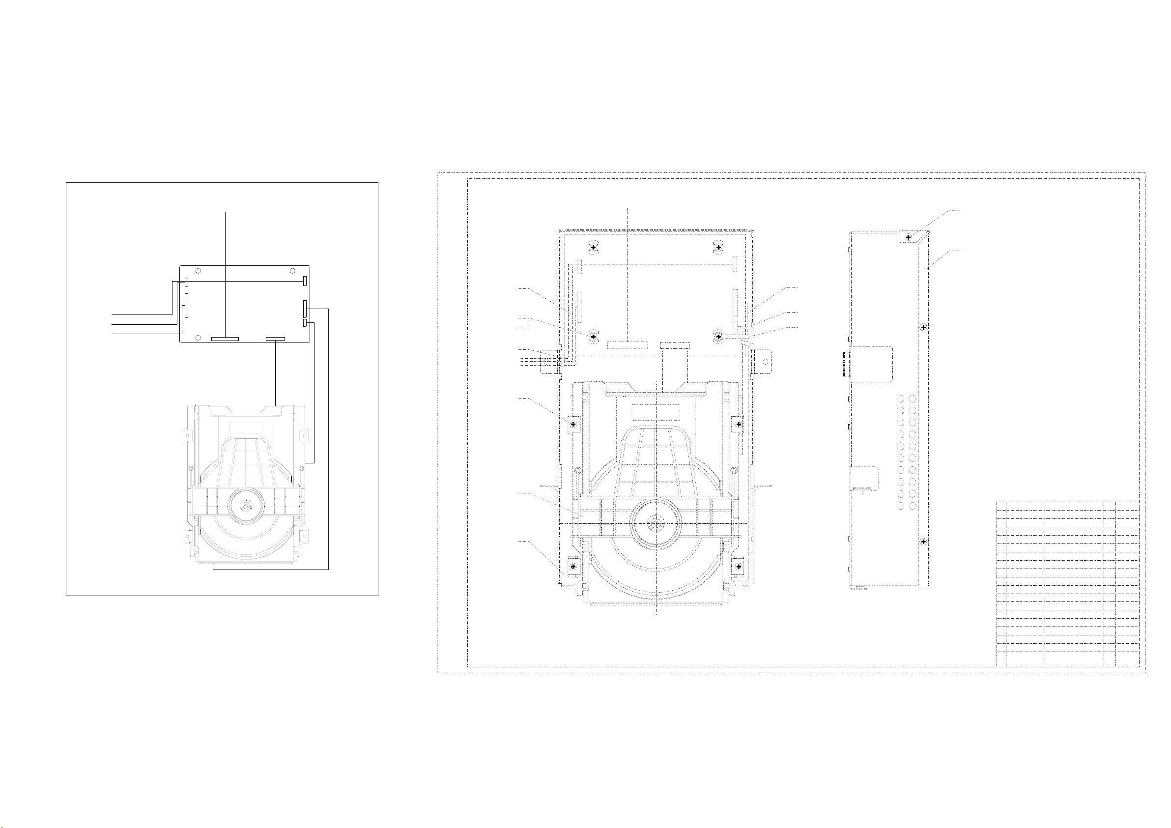
Final Wiring Diagram and Final Assembly Diagram for DVD130A
TO TV
JUV6.604.270
JUV6.604.274
JUV6.604.322
XP4
XP3
TO TV
JUV6.604.272
JUV6.672.287
Decoding board assembly
XP2
CN1
1010
66
Technical RequirementsTechnical Requirements
1. During mounting, ensure static protection1. During mounting, ensure static protection
XP1
44
22
to the disc tray (13).to the disc tray (13).
2. Stick the warning labels (9) conspicuously2. Stick the warning labels (9) conspicuously
on the disc tray (13) and shield coveron the disc tray (13) and shield cover
XS1
XS2
1212
77
33
11
88
(6) respectively.(6) respectively.
3. Fasten the flat cable between the disc3. Fasten the flat cable between the disc
tray and decoding board with the tape (14).tray and decoding board with the tape (14).
4. Bind wire with the wire clip (8).4. Bind wire with the wire clip (8).
5. Ensure that four fins of the shield case 5. Ensure that four fins of the shield case
are not deformed during mounting.are not deformed during mounting.
Flat cable
JUV6.604.291
JUV6.604.290
1111
1313
Disc tray (including disc tray DJ100 and DV-33FS)
Final Wiring Diagram for DVD130A
1818
1717
1616
55
1515
1414
1313
1212
1111
1010
JUV8.817.041JUV8.817.041
99
JU8.667.310JU8.667.310
88
JUV8.072.015JUV8.072.015
77
JUV7.312.004JUV7.312.004
66
JUV7.312.003JUV7.312.003
55
JUV6.672.287JUV6.672.287
44
JUV6.604.291JUV6.604.291
33
JUV6.604.290JUV6.604.290
22
11
JUV6.463.001JUV6.463.001
SerialSerial
No.No.
Code No.Code No.
(DJ100+DV-33FS)(DJ100+DV-33FS)
Disc trayDisc tray
6560 M3X166560 M3X16
ScrewScrew
ScrewScrew
6560 M3X86560 M3X8
Tapping screwTapping screw
Warning labelWarning label
Wire clipWire clip
Supporting columnSupporting column
Shield coverShield cover
Shield caseShield case
Decoding board assemblyDecoding board assembly
Wired connectorWired connector
Wired connectorWired connector
Fastening clip assemblyFastening clip assembly
3X8VTHO3X8VTHO
PartsParts
44
44
66
22
11
44
11
11
11
11
11
11
RemarksRemarks
QtyQty
Final Assembly Diagram of DVD UnitFinal Assembly Diagram of DVD Unit
 Loading...