

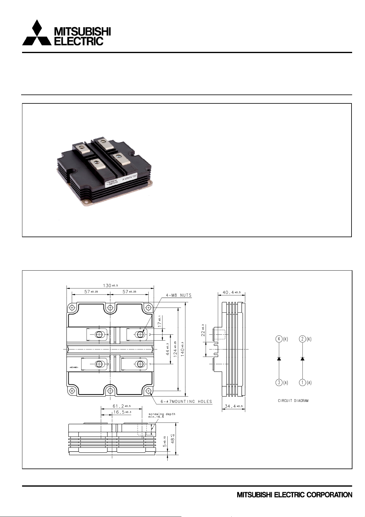
< HIGH VOLTAGE DIODE MODULES >
RM1200DG-90F
HIGH POWER SWITCHING USE
INSULATED TYPE High Voltage Diode Modules
RM1200DG-90F
I
F·································································
V
RRM··························································
1200A
4500V
2-element in a Pack
High insulated Type
Soft Recovery Diode
AlSiC Baseplate
APPLICATION
Traction drives, High Reliability Converters / Inverters, DC choppers
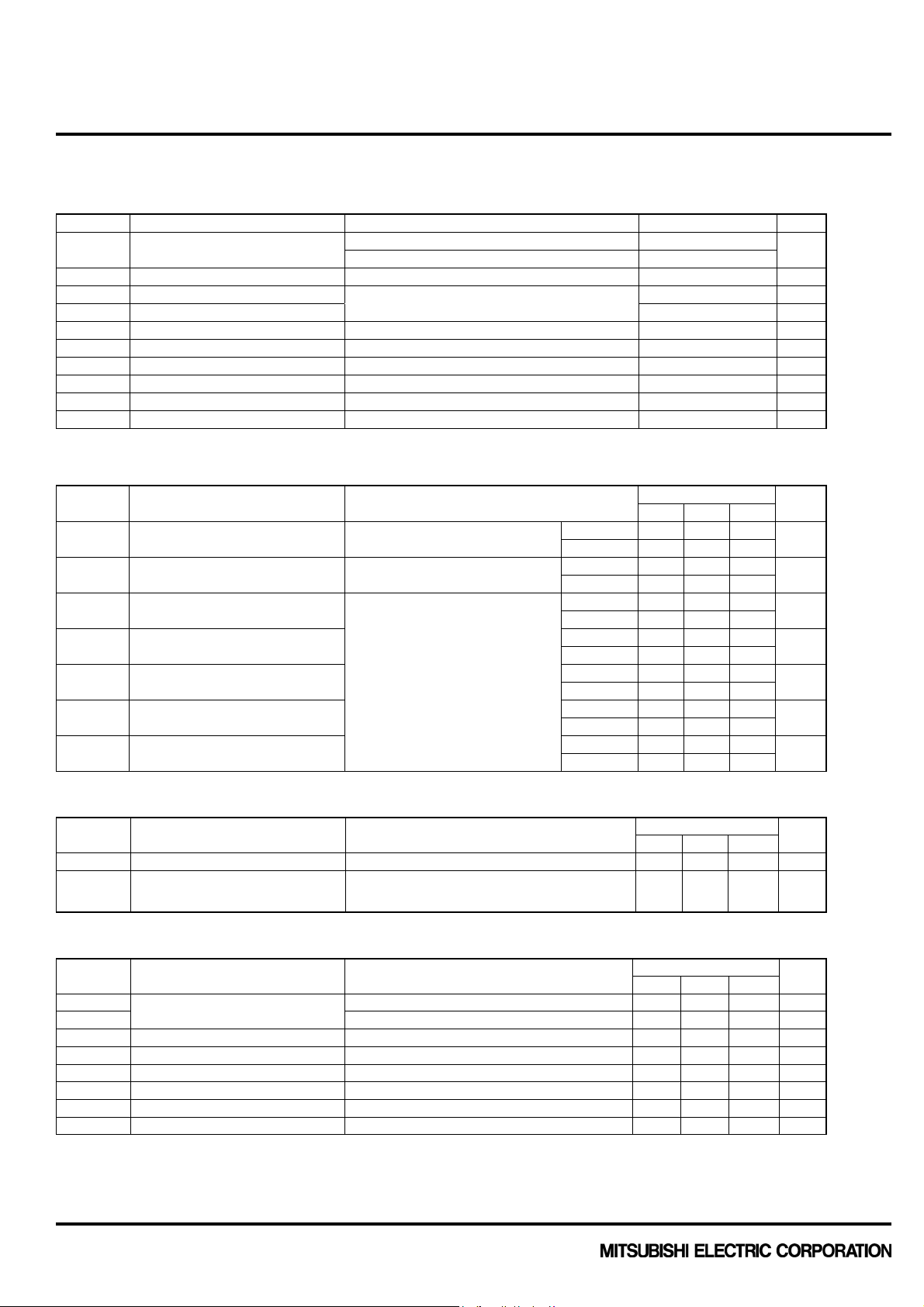
OUTLINE DRAWING & CIRCUIT DIAGRAM Dimensions in mm
December 2012
HVM-2027-B.doc
1
< HIGH VOLTAGE DIODE MODULES >
RM1200DG-90F
HIGH POWER SWITCHING USE
INSULATED TYPE High Voltage Diode Modules
MAXIMUM RATINGS
Symbol Item Conditions Ratings Unit
V
Repetitive peak reverse voltage
RRM
IF Forward current DC, Tc = 65°C 1200 A
I
Surge forward current 9.8 kA
FSM
2
I
Surge current load integral
t
P
Maximum power dissipation Tc = 25°C 6250 W
tot
V
Isolation voltage RMS, sinusoidal, f = 60 Hz, t = 1 min. 10200 V
iso
Ve Partial discharge extinction voltage RMS, sinusoidal, f = 60 Hz, QPD ≤ 10 pC 3500 V
Tj Junction temperature −50 ~ +150 °C
T
Operating junction temperature −50 ~ +125 °C
jop
T
Storage temperature −55 ~ +125 °C
stg
ELECTRICAL CHARACTERISTICS
Symbol Item Conditions
I
Repetitive reverse current VRM = V
RRM
V
FM
trr Reverse recovery time
Irr Reverse recovery current
Q
Reverse recovery charge
r0Hr
E
rec(10%)
E
Reverse recovery energy
rec
THERMAL CHARACTERISTICS
Symbol Item Conditions
R
th(j-c)
R
th(c-s)
Forward voltage IF = 1200 A
Reverse recovery energy
(Note 1)
Thermal resistance Junction to Case (per 1/2 module) — — 20.0 K/kW
Contact thermal resistance
Tj = −40…+125°C 4500
T
= −50°C 4400
j
= 125°C, tp = 10 ms, Half-sine wave, VR = 0 V
T
j_start
480 kA
Limits
Min Typ Max
RRM
Tj = 25°C — — 3.0
T
= 125°C — 9.0 —
j
Tj = 25°C — 2.55 —
Tj = 125°C — 2.85 3.45
Tj = 25°C — 0.70 —
T
= 125°C — 0.90 —
VCC = 2800 V
I
= 1200 A
F
−d
= 3900 A/µs @ Tj = 25°C
i/dt
−d
= 3600 A/µs @ Tj = 125°C
i/dt
L
= 150 nH
s
Inductive load
j
Tj = 25°C — 1050 —
T
= 125°C — 1140 —
j
Tj = 25°C — 990 —
T
= 125°C — 1560 —
j
Tj = 25°C — 1.44 —
Tj = 125°C — 2.25 —
Tj = 25°C — 1.65 —
= 125°C — 2.55 —
T
j
Limits
Min Typ Max
Case to heat sink,
D
= 100 µm (per 1/ 2 module)
(c-s)
grease
= 1 W/m·k
— 16.0 — K/kW
V
Unit
mA
V
µs
A
µC
J
J
Unit
2
s
MECHANICAL CHARACTERISTICS
Symbol Item Conditions
Mt M8 : Main terminals screw 7.0 — 22.0 N·m
Ms
Mounting torque
M6 : Mounting screw 3.0 — 6.0 N·m
m Mass — 1.0 — kg
CTI Comparative tracking index 600 — — —
da Clearance 26.0 — — mm
ds Creepage distance 56.0 — — mm
L
Parasitic stray inductance — 15.0 — nH
P AK
R
Internal lead resistance Tc = 25°C — 0.09 — mΩ
AA’+KK’
Note 1. E
Note 2. Definition of all items is according to IEC 60747, unless otherwise specified.
December 2012
are the integral of 0. 1VR x 0.1IF x dt.
rec(10%)
HVM-2027-B.doc
Limits
Min Typ Max
Unit
2
< HIGH VOLTAGE DIODE MODULES >
RM1200DG-90F
HIGH POWER SWITCHING USE
INSULATED TYPE High Voltage Diode Modules
PERFORMANCE CURVES
FORWARD CHARACTERISTICS
(TYPICAL)
REVERSE RECOVERY ENERGY
CHARACTERISTICS (TYPICAL)
24 00
18 00
12 00
Tj = 25 °C
Tj = 12 5° C
6
VCC = 280 0V
-di/dt = 3 600 A/ µs @1 25° C
LS = 150nH , Tj = 125°C
I ndu cti v e lo ad
4.5
3
E
rec
Forward Current [A]
600
1.5
Reverse Recovery Energy [J]
0
012345
Forward Voltage [V]
REVERSE RECOVERY
CHARACTERISTICS (TYPICAL)
0
0 6 00 12 00 180 0 2 40 0
Forward Current [A]
REVERSE RECOVERY
SAFE OPERATING AREA (RRSOA)
10 0
VCC = 28 00 V
-di/dt = 3600 A/ µs @12 5°C
LS = 1 50n H, Tj = 12 5°C
In d uc t iv e l o a d
10
1
Reverse Recovery Time [µs]
0.1
100 1000 10000
Forward Current [A]
1 0000
I
rr
1 000
t
rr
100
Reverse Recovery Current [A]
10
40 00
VCC 32 00 V, -di/dt < 6kA/ µ s
Tj = 1 25° C
30 00
20 00
10 00
Reverse Recovery Current [A]
0
0 10002000300040005000
Reverse Voltage [V]
December 2012
HVM-2027-B.doc
3
< HIGH VOLTAGE DIODE MODULES >
RM1200DG-90F
HIGH POWER SWITCHING USE
INSULATED TYPE High Voltage Diode Modules
PERFORMANCE CURVES
TRANSIENT THERMAL IMPEDANCE
CHARACTERISTICS
1.2
R
= 20.0K / kW
th(j-c )
1
)t(
t
n
RZ
1i
exp1
i)cj(th
i
0.8
0.6
0.4
0.2
Normalized Transient Thermal impedance
0
0.001 0.01 0.1 1 10
Tim e [s ]
1 2 3 4
Ri [K/kW] 0.0055 0.2360 0.4680 0.2905
ti [sec] 0.0001 0.0131 0.0878 0.6247
December 2012
HVM-2027-B.doc
4
< HIGH VOLTAGE DIODE MODULES >
RM1200DG-90F
HIGH POWER SWITCHING USE
INSULATED TYPE High Voltage Diode Modules
Keep safety first in your circuit designs!
Mitsubishi Electric Corporation puts the maximum effort into making semiconductor products better and more
reliable, but there is always the possibility that trouble may occur with them. Trouble with semiconductors may lead
to personal injury, fire or property damage. Remember to give due consideration to safety when making your circuit
designs, with appropriate measures such as (i) placement of substitutive, auxiliary circuits, (ii) use of
non-flammable material or (iii) prevention against any malfunction or mishap.
Notes regarding these materials
・ These materials are intended as a reference to assist our customers in the selection of the Mitsubishi
semiconductor product best suited to the customer’s application; they do not convey any license under any
intellectual property rights, or any other rights, belonging to Mitsubishi Electric Corporation or a third party.
・ Mitsubishi Electric Corporation assumes no responsibility for any damage, or infringement of any third-party’s
rights, originating in the use of any product data, diagrams, charts, programs, algorithms, or circuit application
examples contained in these materials.
・ All information contained in these materials, including product data, diagrams, charts, programs and
algorithms represents information on products at the time of publication of these materials, and are subject to
change by Mitsubishi Electric Corporation without notice due to product improvements or other reasons. It is
therefore recommended that customers contact Mitsubishi Electric Corporation or an authorized Mitsubishi
Semiconductor product distributor for the latest product information before purchasing a product listed herein.
The information described here may contain technical inaccuracies or typographical errors. Mitsubishi
Electric Corporation assumes no responsibility for any damage, liability, or other loss rising from these
inaccuracies or errors.
・ Please also pay attention to information published by Mitsubishi Electric Corporation by various means,
including the Mitsubishi Semiconductor home page (http://www.MitsubishiElectric.com/
・ When using any or all of the information contained in these materials, including product data, diagrams,
charts, programs, and algorithms, please be sure to evaluate all information as a total system before making
a final decision on the applicability of the information and products. Mitsubishi Electric Corporation assumes
no responsibility for any damage, liability or other loss resulting from the information contained herein.
・ Mitsubishi Electric Corporation semiconductors are not designed or manufactured for use in a device or
system that is used under circumstances in which human life is potentially at stake. Please contact Mitsubishi
Electric Corporation or an authorized Mitsubishi Semiconductor product distributor when considering the use
of a product contained herein for any specific purposes, such as apparatus or systems for transportation,
vehicular, medical, aerospace, nuclear, or undersea repeater use.
・ The prior written approval of Mitsubishi Electric Corporation is necessary to reprint or reproduce in whole or
in part these materials.
・ If these products or technologies are subject to the Japanese export control restrictions, they must be
exported under a license from the Japanese government and cannot be imported into a country other than
the approved destination.
・ Any diversion or re-export contrary to the export control laws and regulations of Japan and/or the country of
destination is prohibited.
・ Please contact Mitsubishi Electric Corporation or an authorized Mitsubishi Semiconductor product distributor
for further details on these materials or the products contained therein.
).
© 2011 MITSUBISHI ELECTRIC CORPORATION. ALL RIGHTS RESERVED.
December 2012
HVM-2027-B.doc
5
 Loading...