

Page 1
MITSUBISHI <INTELLIGENT POWER MODULES>
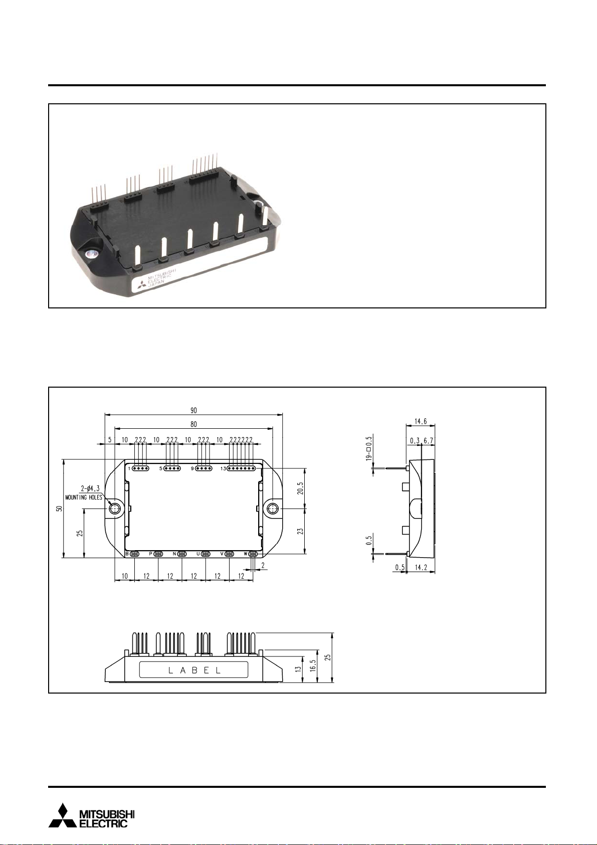
PM75B5L1C060
APPLICATION
PM75B5L1C060
FLAT-BASE TYPE
INSULATED PACKAGE
FEATURE
a) Adopting new 5th generation Full-Gate
TM
CSTBT
b) Error output signal is possible from all
each protection upper and lower IGBT
c) The mounting surface is 90mm×50mm
about 30% less than B5LA type
• Monolithic gate drive & protection logic
• Detection, protection & status indication
circuits for, short-circuit, over-temperature
& under-voltage
chip
Photo voltaic power conditioner
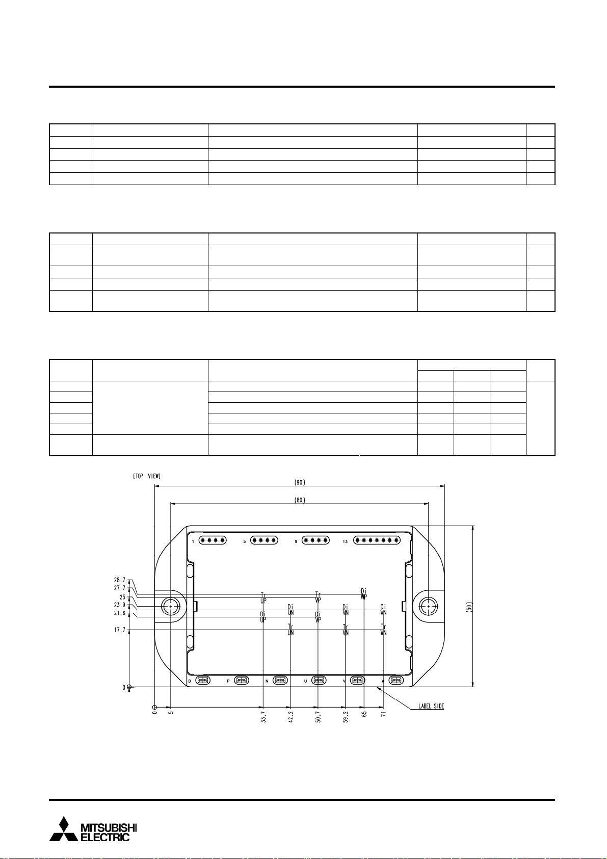
PACKAGE OUTLINES Dimensions in mm
Terminal code
1. VUPC
2. UFo
3. UP
UP1
4. V
5. VVPC
6. VFo
P
7. V
8. VVP1
9. NC
10. NC
11. NC
12
13. VNC
14. V
. NC
N1
15. NC
16. UN
17. VN
18. WN
19. Fo
1
November. 2011
Page 2
MITSUBISHI <INTELLIGENT POWER MODULES>
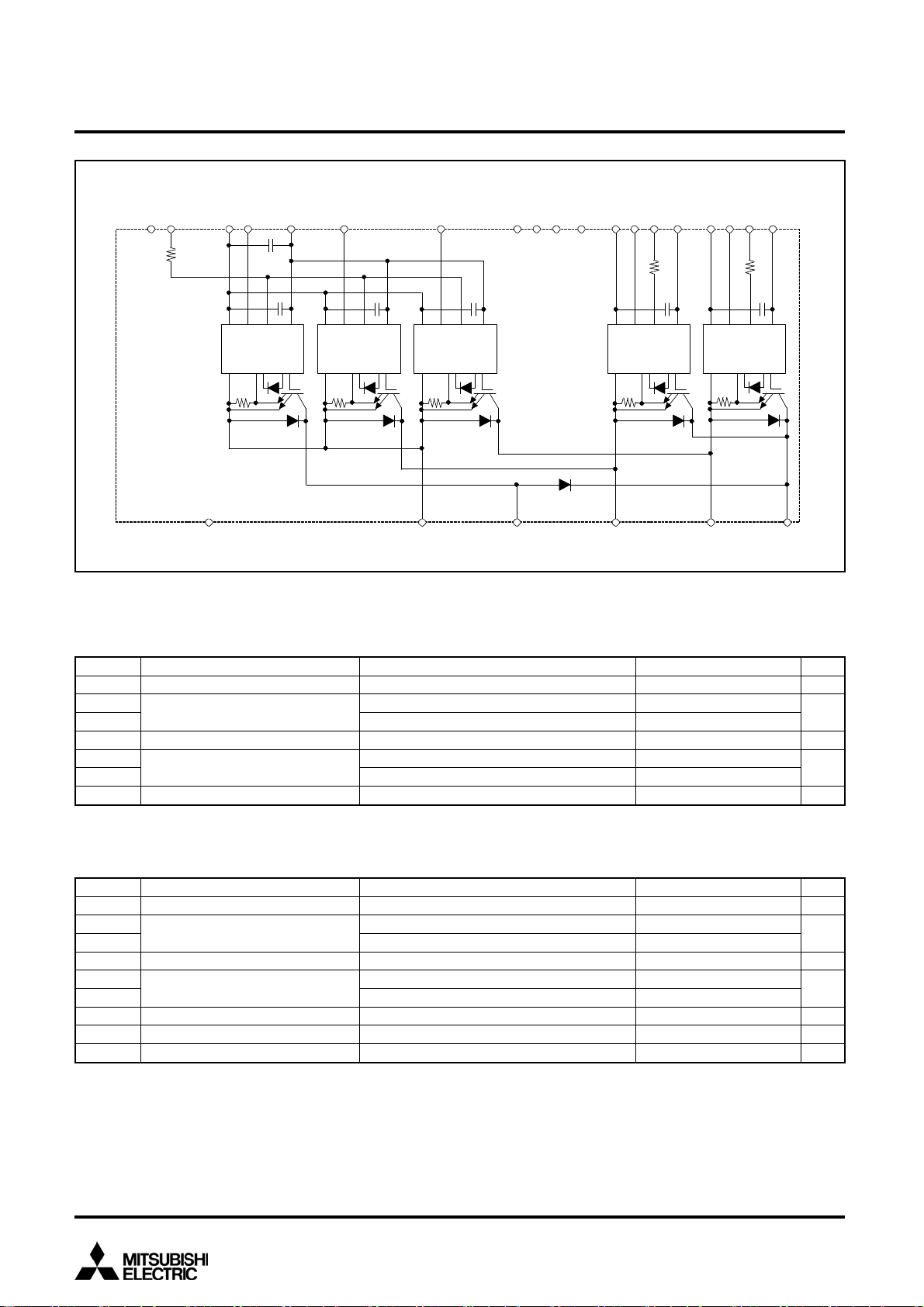
INTERNAL FUNCTIONS BLOCK DIAGRAM
NC Fo
1.5k
V
NCWN
GND SC OT OUT
V
N1
VccFoINGND
V
N
VccFoINGND
GND S C OT OUT
U
N
VccFoINGND
GND SC OT OUT
NC NC NC NC V
PM75B5L1C060
FLAT-BASE TYPE
INSULATED PACKAGE
V
V
P
V
VPC
Fo
1.5k
VccFoINGND
GND SC OT OUT
VP1
U
P
V
U
UPC
GND SC OT OUT
Fo
1.5k
V
UP1
VccFoINGND
PUVWNB
MAXIMUM RATINGS (Tj = 25°C, unless otherwise noted)
INVERTER PART
Symbol Parameter Conditions Ratings Unit
V
Collector-Emitter Voltage VD=15V, V
CES
IC T
I
CRM
P
Total Power Dissipation TC=25°C 201 W
tot
Collector Current
=25°C 75
C
Pulse 150
IE Emitter Current TC=25°C 75
I
(Free wheeling Diode Forward current) Pulse 150
ERM
=15V 600 V
CIN
A
A
Tj Junction Temperature -20 ~ +150 °C
*: Tc measurement point is just under the chip.
CONVERTER PART
Symbol Parameter Conditions Ratings Unit
V
Collector-Emitter Voltage VD=15V, V
CES
IC T
I
CRM
P
Total Power Dissipation TC=25°C 201 W
tot
Collector Current
=25°C 75
C
Pulse 150
IE Emitter Current TC=25°C 75
I
(Free wheeling Diode Forward current) Pulse 150
ERM
IF Di Forward Current TC=25°C 75 A
V
Di Rated DC Reverse Voltage TC=25°C 600 V
R(DC)
Tj Junction Temperature -20 ~ +150 °C
*: Tc measurement point is just under the chip.
=15V 600 V
CIN
A
A
2
November. 2011
Page 3
MITSUBISHI <INTELLIGENT POWER MODULES>
PM75B5L1C060
FLAT-BASE TYPE
INSULATED PACKAGE
CONTROL PART
Symbol Parameter Conditions Ratings Unit
VD Supply Voltage
V
Input Voltage
CIN
VFO Fault Output Supply Voltage
IFO Fault Output Current
Applied between : V
Applied between : U
Applied between : U
Sink current at U
Fo, VFo, Fo terminals
UP1-VUPC
P-V
UPC
Fo-V
UPC
, V
VP1-VVPC,VN1-VNC
, VP-V
VPC
, VFo-V
, UN・VN・WN -V
VPC
, Fo-VNC
NC
20 V
20 V
20 V
20 mA
TOTAL SYSTEM
Symbol Parameter Conditions Ratings Unit
V
CC(PROT)
V
CC(surge)
T
Storage Temperature
stg
V
Isolation Voltage
isol
*: TC measurement point is just under the chip.
Supply Voltage Protected by
SC
Supply Voltage (Surge)
V
=13.5V ~ 16.5V
D
Inverter Part, T
=+125°C Start
j
Applied between : P-N, Surge value
60Hz, Sinusoidal, Charged part to Base plate,
AC 1min, RMS
450 V
500 V
-40 ~ +125 °C
2500 V
THERMAL RESISTANCE
Symbol Parameter Conditions
R
th(j-c)Q
R
th(j-c)D
R
th(j-c)Q
R
th(j-c)D
R
th(j-c)D
R
th(c-s)
Note.1: If you use this value, R
Thermal Resistance
Inverter, IGBT (per 1 element) (Note.1) - - 0.62
Inverter, FWDi (per 1 element) (Note.1) - - 1.06
Converter, IGBT (per 1 element) (Note.1) - - 0.62
Converter, FWDi (per 1 element) (Note.1) - - 1.06
Contact Thermal Resistance
should be measured just under the chips.
th(s-a)
Converter, Di (per 1 element) (Note.1) - - 1.06
Case to heat sink, (per 1 module)
Thermal grease applied (Note.1)
Min. Typ. Max.
Limits
- 0.06 -
Unit
K/W
3
November. 2011
Page 4
MITSUBISHI <INTELLIGENT POWER MODULES>
ELECTRICAL CHARACTERISTICS (Tj = 25°C, unless otherwise noted)
INVERTER PART
Symbol Parameter Conditions
V
CEsat
Collector-Emitter Saturation
Voltage
VEC Emitter-Collector Voltage IE=75A, VD=15V, V
ton
trr
t
c(on)
t
off
t
c(off)
I
CES
Switching Time
Collector-Emitter Cut-off
Current
CONVERTER PART
Symbol Parameter Conditions
V
CEsat
VEC Emitter-Collector Voltage IE=75A, VD=15V, V
VFM Di Forward Voltage IF=75A
ton
trr
t
c(on)
t
off
t
c(off)
I
CES
Collector-Emitter Saturation
Voltage
Switching Time
Collector-Emitter Cut-off
Current
V
=15V, IC=75A
D
V
=0V, Pulsed (Fig. 1)
CIN
= 15V (Fig. 2)
CIN
V
=15V, V
D
V
=300V, IC=75A
CC
T
=125°C
j
=0V←→15V
CIN
Inductive Load (Fig. 3,4)
V
V
V
V
V
T
, VD=15V , V
CE=VCES
=15V, IC=75A
D
=0V, Pulsed (Fig. 1)
CIN
=15V, V
D
=300V, IC=75A
CC
=125°C
j
=0V←→15V
CIN
=15V (Fig. 5)
CIN
= 15V (Fig. 2)
CIN
Inductive Load (Fig. 3,4)
V
CE=VCES
, VD=15V , V
=15V (Fig. 5)
CIN
Tj=25°C
T
=125°C
j
Tj=25°C
T
=125°C
j
Tj=25°C
=125°C
T
j
Tj=25°C
T
=125°C
j
PM75B5L1C060
FLAT-BASE TYPE
INSULATED PACKAGE
Limits
Min. Typ. Max.
- 2.2 2.7
- 2.2 2.7
- 2.4 3.3
0.1 0.5 1.2
- 0.1 0.2
- 0.15 0.3
- 1.1 2.0
- 0.2 0.4
- - 1
- - 10
Limits
Min. Typ. Max.
- 2.2 2.7
- 2.2 2.7
- 2.4 3.3
- 2.4 3.3
0.1 0.5 1.2
- 0.1 0.2
- 0.15 0.3
- 1.1 2.0
- 0.2 0.4
- - 1
- - 10
Unit
V
V
s
mA
Unit
V
V
V
s
mA
CONTROL PART
Symbol Parameter Conditions
ID Circuit Current VD=15V, V
V
Input ON Threshold Voltage 1.2 1.5 1.8
th(ON)
V
Input OFF Threshold Voltage
th(OFF)
Applied between :
CIN
=15V
U
P-V
, VP-V
UPC
VN1-VNC - 6.5 12
V
, UN・VN・WN -V
VPC
- 1.6 4.0
*P1-V*PC
Min. Typ. Max.
NC
1.7 2.0 2.3
SC Short Circuit Trip Level -20≤Tj≤125°C, VD=15V (Fig. 3, 6) 112 - - A
t
off(SC)
OT Trip level 135 - -
OT
(hys)
UVt Trip level 11.5 12.0 12.5
UVr
I
FO(H)
I
FO(L)
Short Circuit Current Delay
Time
Over Temperature Protection Detect Temperature of IGBT chip
Supply Circuit Under-Voltage
Protection
- - 0.01
Fault Output Current V
V
=15V (Fig. 3, 6) - 0.2 - s
D
Hysteresis - 20 -
-20≤Tj≤125°C
=15V, VFO=15V (Note.2)
D
Reset level - 12.5 -
tFO Fault Output Pulse Width VD=15V (Note.2) 1.0 1.8 - ms
Note.2: Fault output is given only when the internal SC, OT & UV protections schemes of either upper or lower arm device operate to protect it.
Limits
- 10 15
Unit
mA
V
°C
V
mA
4
November. 2011
Page 5

MITSUBISHI <INTELLIGENT POWER MODULES>
PM75B5L1C060
FLAT-BASE TYPE
INSULATED PACKAGE
MECHANICAL RATINGS AND CHARACTERISTICS
Symbol Parameter Conditions
Min. Typ. Max.
Ms Mounting Torque Mounting part screw : M4 1.4 1.65 1.9 N・m
m Weight - - 135 - g
RECOMMENDED CONDITIONS FOR USE
Symbol Parameter Conditions Recommended value Unit
VCC Supply Voltage Applied across P-N terminals ≤ 450 V
VD Control Supply Voltage
V
Input ON Voltage ≤ 0.8
CIN(ON)
V
Input OFF Voltage
CIN(OFF)
f
PWM Input Frequency Using Application Circuit of Fig. 8 ≤ 20 kHz
PWM
t
dead
Arm Shoot-through Blocking
Time
Applied between : V
V
Applied between :
U
For IPM’s each input signals (Fig. 7)
IO Module Operating Current RMS ≤ 30 A
Note.3: With ripple satisfying the following conditions: dv/dt swing ≤ ±5V/μs, Variation ≤ 2V peak to peak
,
UP1-VUPC
VP1-VVPC,VN1-VNC
P-V
, VP-V
UPC
VPC
(Note.3)
, UN・VN・WN -V
NC
Limits
15.0±1.5 V
≥ 9.0
≥ 2.0 s
Unit
V
5
November. 2011
Page 6

MITSUBISHI <INTELLIGENT POWER MODULES>
PM75B5L1C060
FLAT-BASE TYPE
INSULATED PACKAGE
PRECAUTIONS FOR TESTING
1. Before applying any control supply voltage (VD), the input terminals should be pulled up by resistors, etc. to their
corresponding supply voltage and each input signal should be kept off state.
After this, the specified ON and OFF level setting for each input signal should be done.
2. When performing “SC” tests, the turn-off surge voltage spike at the corresponding protection operation should not be
allowed to rise above V
(These test should not be done by using a curve tracer or its equivalent.)
Fo
Vcin
GND
GND
VD(all)
VD(all)
VD(all)
Fo
Vcin
Fo
Vcin
Vcc
Fo
IN
Vcc
Fo
IN
rating of the device.
CES
GND
Vcc
Fo
IN
Fig. 1 V
CEsat
P
VD(all)
Vcc
VD(all)
U,V,W
N
Ic
U,V,(N)
Test
Fo
Vcin
Fo
Vcin
P,(U ,V,W)
Vcc
Fo
IN
GND
Vcc
Fo
IN
GND
Vcc
Fo
V
Ic
VD(all)
Fo
Vcin
IN
GND
U,V,W,(N)
P,(U ,V,W)
V
IE , I
F
Fig. 2 VEC, VFM Te st
P
U,V
Vcc
N
Ic
Fig. 3 Switching time and SC test circuit
Fig. 4 Switching time test waveform
P,(U ,V,W)
A
V
CE
puls e
GND
Vcc
VD(all)
Fo
Fo
IN
Vcin
Fig. 5 I
CES
U,V,W,(N)
Test
Fig. 6 SC test waveform
Fig. 7 Dead time measurement point example
6
November. 2011
Page 7

MITSUBISHI <INTELLIGENT POWER MODULES>
A
PM75B5L1C060
FLAT-BASE TYPE
INSULATED PACKAGE
P
U
C Out put
V
W
N
B
1.5k
1.5k
OUT
Vcc
OT
Fo
SC
IN
GND GND
OUT
Vcc
OT
Fo
SC
IN
GND GND
OUT
Vcc
OT
Fo
SC
IN
GND GND
OUT
Vcc
OT
Fo
SC
IN
GND GND
OUT
Vcc
OT
Fo
SC
IN
GND GND
VD3
VD1
VD2
20k
≥0.1µ
20k
≥0.1µ
20k
≥0.1µ
20k
≥0.1µ
20k
≥0.1µ
≥10µ
≥10µ
≥10µ
≥10µ
≥10µ
V
U
U
V
V
V
V
V
NC
NC
NC
NC
U
V
V
W
V
UP1
Fo
P
UPC
VP1
Fo
P
VPC
N
N
N1
N
NC
1.5k
Fo
NC
Fig. 8 Application Example Circuit
NOTES FOR STABLE AND SAFE OPERATION ;
• Design the PCB pattern to minimize wiring length between opto-coupler and IPM’s input terminal, and also to minimize the
stray capacity between the input and output wirings of opto-coupler.
• Connect low impedance capacitor between the Vcc and GND terminal of each fast switching opto-coupler.
• Fast switching opto-couplers: t
PLH
, t
≤ 0.8μs, Use High CMR type.
PHL
• Slow switching opto-coupler: CTR > 100%
• Use 3 isolated control power supplies (V
). Also, care should be taken to minimize the instantaneous voltage charge of the
D
power supply.
• Make inductance of DC bus line as small as possible, and minimize surge voltage using snubber capacitor between P and N
terminal.
7
November. 2011
Page 8

MITSUBISHI <INTELLIGENT POWER MODULES>
j
PERFORMANCE CURVES
OUTPUT CHARACTERISTICS
INVERTER PART & CONVERTER PART
80
Tj=25°C
70
60
(A)
C
50
40
30
20
COLLECTOR CURRENT I
10
0
0.5 1. 0 1.5 2.0 2.5
COLLECTOR-EMITTER VOLTAGE V
COLLECTOR-EMITTER SATURATION
VOLTAGE (VS. V
INVERTER PART & CONVERTER PART
2.5
(V)
CEsat
2.0
(TYPICAL)
VD=17V
) CHARACTERISTICS
D
(TYPICAL)
VD=13V
VD=15V
(V)
CE
PM75B5L1C060
FLAT-BASE TYPE
INSULATED PACKAGE
COLLECTOR-EMITTER SATURATION
VOLTAGE (VS. Ic) CHARACTERISTICS
(TYPICAL)
INVERTER PART & CONVERTER PART
2.5
2.0
(V)
CEsat
1.5
1.0
COLLECTOR-EMITTER
0.5
SATURATION VOLTAGE V
0.0
0 1020304050607080
COLLECTOR CURRENT IC (A)
FREE WHEELING DIODE & DIODE
FORWARD CHARACTERISTICS
(TYPICAL)
INVERTER PART & CONVERTER PART
80
VD=15V
70
(A)
60
F
(A)
E
50
Tj=25°C
=125°C
T
VD=15V
Tj=25°C
Tj=125°C
40
1.5
COLLECTO R-EMITTER
Ic=75A
Tj=25°C
Tj=125°C
SATURATION VOLTAGE V
1.0
12 13 14 15 16 17 18
CONTROL VOLTAGE V
(V) EMITTER-COLLECTOR VOLTAGE VEC (V)
D
30
20
EMITTER CURRENT I
Di FORWARD CURRENT I
10
0
00.511.522.5
Di FORWARD VOLTAGE V
FM
(V)
8
November. 2011
Page 9

MITSUBISHI <INTELLIGENT POWER MODULES>
SWITCHING TIME (t
INVERTER PART & CONVERTER PART
10
Vcc=300V
VD=15V
Tj=25°C
(μs)
off
, t
on
1
Tj=125°C
Inductive Load
toff
ton
SWITCHING TIME t
0.1
110100
COLLECTOR CURRENT I
SWITCHING ENERGY CHARACTERISTICS
1.6
Vcc=300V
1.4
VD=15V
1.2
(mJ/pulse)
off
1.0
, E
on
0.8
0.6
0.4
0.2
SWITCHING ENERGY E
0.0
Tj=25°C
Tj=125°C
Inductive Load
0 20406080
COLLECTOR CURRENT I
, t
) CHARACTERISTICS
on
off
(TYPICAL)
(TYPICAL)
INVERTER PART
PM75B5L1C060
INSULATED PACKAGE
SWITCHING TIME (t
INVERTER PART & CONVERTER PART
1
tc(off)
(μs)
c(off)
, t
c(on)
0.1
SWITCHING TIME t
0.01
(A) COLLECTOR CURRENT IC (A)
C
tc(on)
Vcc=300V
VD=15V
Tj=25°C
Tj=125°C
Inductive Load
110100
SWITCHING ENERGY CHARACTERISTICS
CONVERTER PART
1.8
Vcc=300V
1.6
VD=15V
Tj=25°C
Tj=125°C
Inductive Load
0 20406080
COLLECTOR CURRENT IC (A)
C
(A)
Eon
Eoff
1.4
(mJ/pulse)
off
1.2
, E
on
1.0
0.8
0.6
0.4
0.2
SWITCHING ENERGY E
0.0
, t
) CHARACTERISTICS
c(on)
c(off)
(TYPICAL)
(TYPICAL)
Eoff
FLAT-BASE TYPE
Eon
9
November. 2011
Page 10

MITSUBISHI <INTELLIGENT POWER MODULES>
FREE WHEELING DIODE
REVERSE RECOVERY CHARACTERISTICS
REVERSE RECOVERY CHARACTERISTICS
(TYPICAL)
INVERTER PART
0.20
Vcc=300V
VD=15V
0.18
(μs)
rr
0.16
0.14
0.12
0.10
0.08
Tj=25°C
Tj=125°C
Inductive Load
REVERSE RECOVERY TIME t
0.06
0 20406080
80
70
Irr
60
50
40
30
trr
20
10
(A)
rr
REVERSE RECOVERY CURRENT I
0.20
0.18
(μs)
rr
0.16
0.14
0.12
0.10
0.08
REVERSE RECOVERY TIME t
0.06
EMITTER CURRENT IE (A) EMITTER CURRENT IE (A)
FREE WHEELING DIODE
REVERSE RECOVERY ENERGY
CHARACTERISTICS
(TYPICAL)
INVERTER PART
1.4
1.2
(mJ/pulse)
rr
1.0
0.8
0.6
0.4
Vcc=300V
VD=15V
Tj=25°C
Tj=125°C
Inductive Load
1.2
1.0
(mJ/pulse)
rr
0.8
0.6
0.4
FREE WHEELING DIODE
(TYPICAL)
CONVERTER PART
Vcc=300V
VD=15V
Tj=25°C
Tj=125°C
Inductive Load
0 20406080
FREE WHEELING DIODE
REVERSE RECOVERY ENERGY
CHARACTERISTICS
(TYPICAL)
CONVERTER PART
Vcc=300V
VD=15V
Tj=25°C
Tj=125°C
Inductive Load
PM75B5L1C060
FLAT-BASE TYPE
INSULATED PACKAGE
45
(A)
40
rr
35
Irr
30
25
trr
20
15
REVERSE RECOVERY CURRENT I
10
0.2
0.0
REVESE RECOVERY ENERGY E
020406080
EMITTER CURRENT I
0.2
0.0
REVESE RECOVERY ENERGY E
0 20406080
(A) EMITTER CURRENT IE (A)
E
10
November. 2011
Page 11

MITSUBISHI <INTELLIGENT POWER MODULES>
I
(mA)
D
I
VS. fc CHARACTERISTICS
D
(TYPICAL)
40
VD=15V
35
30
25
20
15
10
5
0
0 5 10 15 20 25
Tj=25°C
Tj=125°C
(kHz)
f
c
N side
P side
PM75B5L1C060
UV TRIP LEVEL VS. Tj CHARACTERISTICS
20
18
16
14
12
(V)
r
10
/ UV
t
8
UV
6
4
2
0
-50 0 50 100 150
(TYPICAL)
UVt
UVr
Tj (°C)
FLAT-BASE TYPE
INSULATED PACKAGE
SC TRIP LEVEL VS. T
INVERTER PART & CONVERTER PART
2.0
SC
1.8
1.6
1.4
1.2
1.0
0.8
=25°C is normalized 1)
j
0.6
0.4
(SC of T
0.2
0.0
VD=15V
-50 0 50 100 150
CHARACTERISTICS
j
(TYPICAL)
T
(°C)
j
11
November. 2011
Page 12

MITSUBISHI <INTELLIGENT POWER MODULES>
TRANSIENT THERMAL
th(j-c)
NORMALIZED TRANSIENT
THERMAL IMPEDANCE Z
IMPEDANCE CHARACTERISTICS
INVERTER PART
1
0.1
0.01
0.001
0.00001 0.0001 0.001 0.01 0.1 1 10
Single Pulse
IGBT Part;
Per unit base: Rth(j-c)Q=0.62 K/W
FWDi Part;
Per unit base: Rth(j-c)D=1.06K/W
TIME t (sec)
1
th(j-c)
0.1
0.01
NORMALIZED TRANSIENT
THERMAL IMPEDANCE Z
0.001
0.00001 0.0001 0.001 0.01 0.1 1 10
PM75B5L1C060
FLAT-BASE TYPE
INSULATED PACKAGE
TRANSIENT THERMAL
IMPEDANCE CHARACTERISTICS
CONVERTER PART
Single Pulse
IGBT Part;
Per unit base: Rth(j-c)Q=0.62 K/W
FWDi Part;
Per unit base: Rth(j-c)D=1.06K/W
Di part
Per unit base: Rth(j-c)D=1.06K/W
TIME t (sec)
12
November. 2011
 Loading...