

Page 1
PM100RL1A120
MITSUBISHI <INTELLIGENT POWER MODULES>
PM100RL1A120
FLAT-BASE TYPE
INSULATED PACKAGE
FEATURE
Inverter + Brake + Drive & Protection IC
a) Adopting new 5th generation Full-Gate CSTBT
TM
chip
b) The over-temperature protection which detects the chip sur-
TM
face temperature of CSTBT
is adopted.
c) Error output signal is possible from all each protection up-
per and lower arm of IPM.
d) Compatible L-series package.
•3φ 100A, 1200V Current-sense and temperature sense
IGBT type inverter
• Monolithic gate drive & protection logic
• Detection, protection & status indication circuits for, shortcircuit, over-temperature & under-voltage (P-F
O available
from upper arm devices)
• UL Recognized
APPLICATION
General purpose inverter, servo drives and other motor controls
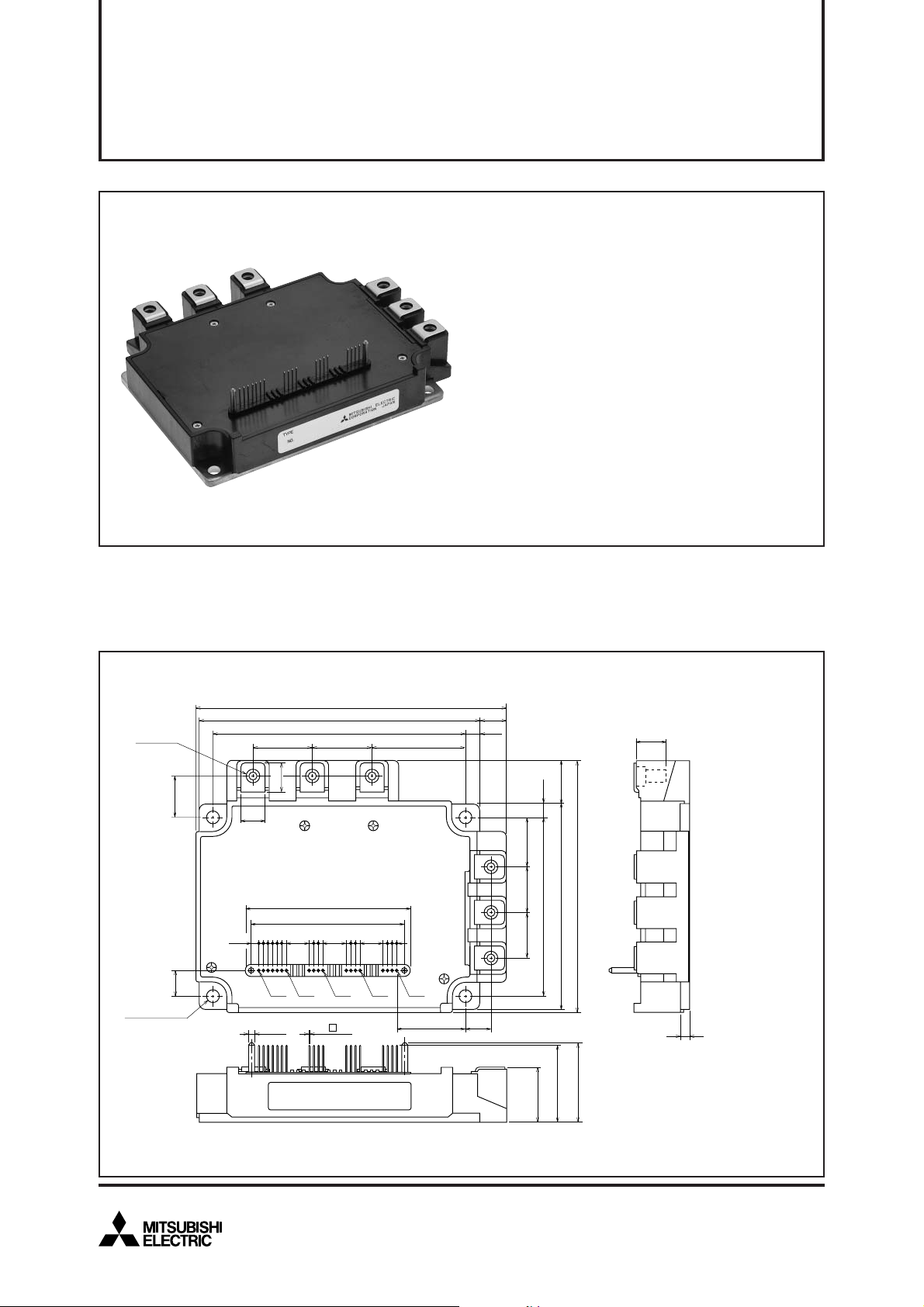
PACKAGE OUTLINES Dimensions in mm
135
6-M5 Nuts
122.1
110±
26 26 40.5
0.5
11.7
6.05
(Screwing Depth)
13
18
11
4-φ5.5
Mounting Holes
(13)
WV U
10.5
71.5
66.5
3.25
6-2 3-2
10
19
2-φ2.5
13
19- 0.5
3-2 3-2
10 10
9 5 1
LABEL
30.15 11
1
18.7
6.05
B
N
P
20 20 21.5
+1
-0.5
24.1
78±0.5
90.1
33.6
110
Te rminal code
1. VUPC
34.7
2. UFO
3. UP
4. VUP1
5. VVPC
6. VFO
7. VP
8. VVP1
9. VWPC
10. WFO
4
11. WP
12. VWP1
13. VNC
14. VN1
15. Br
16. UN
17. VN
18. WN
19. Fo
May 2009
Page 2
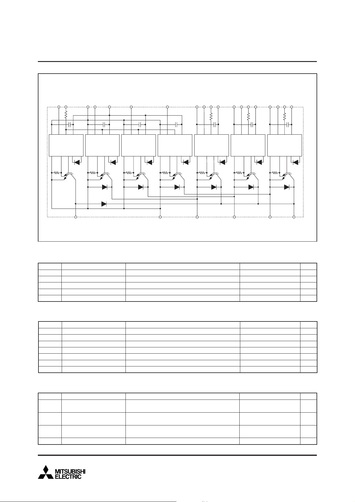
INTERNAL FUNCTIONS BLOCK DIAGRAM
V
Br
Fo
V
NC
V
N1
W
N
N
MITSUBISHI <INTELLIGENT POWER MODULES>
PM100RL1A120
FLAT-BASE TYPE
INSULATED PACKAGE
WPV
U
N
V
WPC
WF
WP1
O
V
VPC
VPV
VF
VP1
O
V
UPC
UPV
UF
UP1
O
1.5k
Gnd In Fo Vcc
Gnd Si Out OT
Gnd In Fo Vcc
Gnd Si Out OT
BNWVUP
Gnd In Fo Vcc
Gnd Si Out OT
Gnd In Fo Vcc
Gnd Si Out OT
1.5k 1.5k 1.5k
Gnd In Fo Vcc
Gnd Si Out OT
Gnd In Fo Vcc
Gnd Si Out OT
Gnd In Fo Vcc
Gnd Si Out OT
MAXIMUM RATINGS (Tj = 25°C, unless otherwise noted)
INVERTER PART
Symbol Parameter Condition Ratings Unit
VCES
±IC
±ICP
PC
Tj
Collector-Emitter Voltage
Collector Current
Collector Current (Peak)
Collector Dissipation
Junction Temperature
*: TC measurement point is just under the chip.
V
D = 15V, VCIN = 15V
T
C = 25°C (Note-1)
T
C = 25°C
T
C = 25°C (Note-1)
1200
100
200
657
–20 ~ +150
V
A
A
W
°C
BRAKE PART
Symbol Parameter Condition Ratings Unit
VCES
IC
ICP
PC
IF
VR(DC)
Tj
Collector-Emitter Voltage
Collector Current
Collector Current (Peak)
Collector Dissipation
FWDi Forward Current
FWDi Rated DC Reverse Voltage
Junction Temperature
V
D = 15V, VCIN = 15V
T
C = 25°C (Note-1)
T
C = 25°C
T
C = 25°C (Note-1)
T
C = 25°C
T
C = 25°C
1200
50
100
446
50
1200
–20 ~ +150
CONTROL PART
Symbol
VD
VCIN
V
FO
IFO
Supply Voltage
Input Voltage
Fault Output Supply Voltage
Fault Output Current
Parameter Condition Ratings Unit
Applied between : V
Applied between : UP-VUPC, VP-VVPC, WP-VWPC
Applied between : UFO-VUPC, VFO-VVPC, WFO-VWPC
Sink current at UFO, VFO, WFO, FO terminals
UP1-VUPC, VVP1-VVPC
VWP1-VWPC, VN1-VNC
UN • VN • WN • Br-VNC
FO-VNC
20
20
20
20
May 2009
2
V
A
A
W
A
V
°C
V
V
V
mA
Page 3
TOTAL SYSTEM
Symbol
V
CC(PROT)
V
CC(surge)
Tstg
Viso
Parameter
Supply Voltage Protected by
SC
Supply Voltage (Surge)
Storage Temperature
Isolation Voltage
V
D = 13.5 ~ 16.5V
Inverter Part, T
Applied between : P-N, Surge value
60Hz, Sinusoidal, Charged part to Base, AC 1 min.
Condition
j = +125°C Start
THERMAL RESISTANCES
Symbol
Rth(j-c)Q
Rth(j-c)F
Rth(j-c)Q
Rth(j-c)F
Rth(c-f)
Junction to case Thermal
Resistances
Contact Thermal Resistance
Parameter
Inverter IGBT part (per 1 element) (Note-1)
Inverter FWDi part (per 1 element) (Note-1)
Brake IGBT part (Note-1)
Brake FWDi upper part (Note-1)
Case to fin, (per 1 module)
Thermal grease applied (Note-1)
* If you use this value, Rth(f-a) should be measured just under the chips.
Condition
MITSUBISHI <INTELLIGENT POWER MODULES>
PM100RL1A120
FLAT-BASE TYPE
INSULATED PACKAGE
Min.
—
—
—
—
—
Ratings
800
1000
–40 ~ +125
2500
Limits
Typ. Max.
—
—
—
—
—
0.023
0.19
0.31
0.28
0.48
Unit
V
V
°C
V
rms
Unit
°C/W
(Note-1) T
axis
C (under the chip) measurement point is below.
arm
X
Y
IGBT
24.5
57.0
UP
FWDi
24.5
46.6
VP WP UN VN WN BR
IGBT
FWDi
IGBT
58.0
58.0
88.0
57.0
46.6
57.0
FWDi
88.0
46.6
IGBT
39.0
28.4
FWDi
39.0
38.8
X
Bottom view
ELECTRICAL CHARACTERISTICS (Tj = 25°C, unless otherwise noted)
INVERTER PART
Symbol
CE(sat)
V
VEC
ton
trr
tc(on)
toff
tc(off)
ICES
Parameter
Collector-Emitter Saturation
Voltage
FWDi Forward Voltage
Switching Time
Collector-Emitter Cutoff
Current
D = 15V, IC = 100A
V
V
CIN = 0V, Pulsed (Fig. 1)
–I
C = 100A, VD = 15V, VCIN = 15V (Fig. 2)
D = 15V, VCIN = 0V↔15V
V
V
CC = 600V, IC = 100A
T
j = 125°C
Inductive Load (Fig. 3,4)
VCE = V
CES
, VD = 15V
Condition
(Fig. 5)
IGBT
72.5
28.4
Y
FWDi
72.5
38.8
T
j = 25°C
T
j = 125°C
T
j = 25°C
T
j = 125°C
IGBT
FWDi
102.5
102.5
28.4
38.8
Min. Typ. Max.
—
—
—
0.3
—
—
—
—
—
—
(unit : mm)
IGBT
12.2
27.6
Limits
1.65
1.85
2.3
0.8
0.3
0.4
1.2
0.4
—
—
Di
6.8
61.0
2.15
2.35
3.3
2.0
0.8
1.0
2.8
1.2
10
Unit
V
V
µs
1
mA
May 2009
3
Page 4

MITSUBISHI <INTELLIGENT POWER MODULES>
PM100RL1A120
FLAT-BASE TYPE
INSULATED PACKAGE
BRAKE PART
—
—
—
—
—
—
—
1.2
1.7
200
100
—
135
—
11. 5
—
—
—
1.0
Limits
1.65
1.85
2.3
—
—
Limits
1.5
2.0
—
—
0.2
—
20
12.0
12.5
—
10
1.8
Unit
2.15
2.35
3.3
10
Max.
8
2
1.8
2.3
—
—
—
—
—
12.5
—
0.01
—
16
15
V
V
1
mA
Unit
mA
4
V
A
µs
°C
V
mA
ms
Symbol
VCE(sat)
VEC
ICES
Parameter
Collector-Emitter Saturation
Voltage
FWDi Forward Voltage
Collector-Emitter Cutoff
Current
VD = 15V, IC = 50A
V
CIN = 0V, Pulsed (Fig. 1)
–I
C = 50A, VCIN = 15V, VD = 15V (Fig. 2)
VCE = V
CES
, VD = 15V
Condition
(Fig. 5)
T
j = 25°C
T
j = 125°C
T
j = 25°C
T
j = 125°C
Min. Typ. Max.
CONTROL PART
Symbol
ID
V
th(ON)
Vth(OFF)
SC
t
off(SC)
OT
OT
UV
UV
IFO(H)
IFO(L)
tFO
Circuit Current
Input ON Threshold Voltage
Input OFF Threshold Voltage
Short Circuit Trip Level
Short Circuit Current Delay
Time
Over Temperature Protection
(hys)
Supply Circuit Under-Voltage
Protection
r
Fault Output Current
Minimum Fault Output Pulse
Width
(Note-2) Fault output is given only when the internal SC, OT & UV protections schemes of either upper or lower arm device operate to
protect it.
Parameter
Condition
D = 15V, VCIN = 15V
V
Applied between : U
P-VUPC, VP-VVPC, WP-VWPC
VN1-VNC
V*P1-V*PC
UN • VN • WN • Br-VNC
–20 ≤ T
j ≤ 125°C, VD = 15V (Fig. 3,6)
D = 15V (Fig. 3,6)
V
Detect Temperature of IGBT chip
–20 ≤ Tj ≤ 125°C
D = 15V, VCIN = 15V (Note-2)
V
D = 15V (Note-2)
V
Inverter part
Brake part
Trip level
Hysteresis
Trip level
Reset level
Min. Typ.
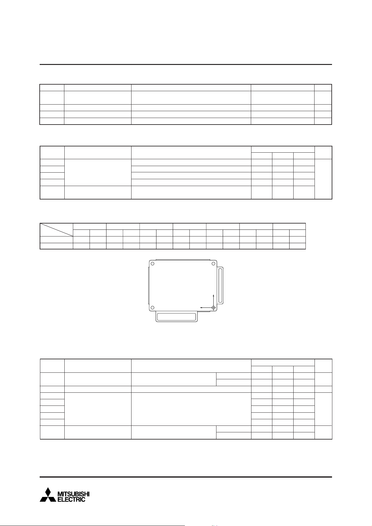
MECHANICAL RATINGS AND CHARACTERISTICS
Symbol
—
—
Parameter
Mounting torque
Weight
Mounting part screw : M5
Main terminal part screw : M5
Condition
—
Min.
2.5
2.5
—
RECOMMENDED CONDITIONS FOR USE
Symbol Parameter
VCC
VD
VCIN(ON)
VCIN(OFF)
fPWM
t
dead
Supply Voltage
Control Supply Voltage
Input ON Voltage
Input OFF Voltage
PWM Input Frequency
Arm Shoot-through
Time
Blocking
Applied across P-N terminals
Applied between : V
Applied between : U
Using Application Circuit of Fig. 8
For IPM’s each input signals (Fig. 7) ≥ 2.5
Condition
UP1-VUPC, VVP1-VVPC
VWP1-VWPC, VN1-VNC (Note-3)
P-VUPC, VP-VVPC, WP-VWPC
UN • VN • WN • Br-VNC
(Note-3) With ripple satisfying the following conditions: dv/dt swing ≤ ±5V/µs, Variation ≤ 2V peak to peak
≤ ± 5V/µs
≤
2V
15V
GND
Recommended value
Limits
Typ.
3.0
3.0
800
≤ 800
15.0 ± 1.5
≤ 0.8
≥ 9.0
≤ 20
Max.
3.5
3.5
—
Unit
N • m
N • m
g
Unit
V
V
V
kHz
µs
May 2009
4
Page 5

MITSUBISHI <INTELLIGENT POWER MODULES>
PM100RL1A120
FLAT-BASE TYPE
INSULATED PACKAGE
PRECAUTIONS FOR TESTING
1. Before applying any control supply voltage (V
sponding supply voltage and each input signal should be kept off state.
After this, the specified ON and OFF level setting for each input signal should be done.
2. When performing “SC” tests, the turn-off surge voltage spike at the corresponding protection operation should not be allowed to rise above V
CES rating of the device.
(These test should not be done by using a curve tracer or its equivalent.)
P, (U,V,W,B)
D), the input terminals should be pulled up by resistors, etc. to their corre-
P, (U,V,W,B)
V
(0V)
IN
V
Fo
D (all)
CIN
V V
U,V,W,B, (N) U,V,W,B, (N)
Ic
V
(15V)
CIN
IN
Fo
VD (all)
Fig. 1 VCE(sat) Test Fig. 2 VEC, (VFM) Test
a) Lower Arm Switching
Signal input
VCIN
(Upper Arm)
(15V)
VCIN
Signal input
(Lower Arm)
b) Upper Arm Switching
VCIN
(15V)
Signal input
(Upper Arm)
Signal input
(Lower Arm)
VCIN
Fo
Fo
D (all)
V
Fo
Fo
D (all)
V
P
U,V,W
N
P
U,V,W
N
trr
Vcc
CS
Ic
Vcc
CS
Ic
90%
10%
tc(on)
V
CIN
(ton = td(on) + tr) (toff = td(off) + tf)
Irr
10% 10%
trtd(on)
Fig. 3 Switching Time and SC Test Circuit Fig. 4 Switching Time Test Waveform
VCIN
(15V)
P, (U,V,W,B)
IN
Fo
U,V,W,B, (N)
VD (all)
Fig. 5 ICES Test
VCIN
A
Pulse
VCE
Ic
Fo
Short Circuit Current
Constant Current
toff(SC)
Fig. 6 SC Test Waveform
Ic
td(off)
tc(off)
–Ic
90%
tf
SC Trip
10%
V
CE
IPM’ input signal V
(Upper Arm)
IPM’ input signal V
(Lower Arm)
1.5V: Input on threshold voltage Vth(on) typical value, 2V: Input off threshold voltage Vth(off) typical value
CIN
0V
CIN
0V
1.5V 1.5V
2V
2V
1.5V
2V
tdeadtdeadtdead
Fig. 7 Dead time measurement point example
5
t
t
May 2009
Page 6

MITSUBISHI <INTELLIGENT POWER MODULES>
PM100RL1A120
FLAT-BASE TYPE
INSULATED PACKAGE
VD
VD
VD
VD
≥10µ
20k
→
IF
≥0.1µ
20k
→
IF
≥0.1µ
20k
→
IF
≥0.1µ
20k
≥0.1µ
4.7k
5V
→
IF
→
IF
1k
≥10µ
≥10µ
≥10µ
VUP1
UFo
UP
VUPC
VVP1
VFo
VP
VVPC
VWP1
WFo
WP
VWPC
UN
VN
VN1
WN
VNC
Br
Fo
1.5k
1.5k
1.5k
1.5k
Vcc
Fo
In
Vcc
Fo
In
Vcc
Fo
In
Vcc
Fo
In
Vcc
Fo
In
Vcc
Fo
In
GND
Vcc
Fo
In
GND
OT
OUT
Si
GNDGND
OT
OUT
Si
GNDGND
OT
OUT
Si
GNDGND
OT
OUT
Si
GNDGND
OT
OUT
Si
GNDGND
OT
OUT
Si
GND
OT
OUT
Si
GND
P
+
–
U
V
W
N
B
M
: Interface which is the same as the U-phase
Fig. 8 Application Example Circuit
NOTES FOR STABLE AND SAFE OPERATION ;
Design the PCB pattern to minimize wiring length between opto-coupler and IPM’s input terminal, and also to minimize the
•
stray capacity between the input and output wirings of opto-coupler.
Connect low impedance capacitor between the Vcc and GND terminal of each fast switching opto-coupler.
•
Fast switching opto-couplers: tPLH, tPHL ≤ 0.8µs, Use High CMR type.
•
Slow switching opto-coupler: CTR > 100%
•
Use 4 isolated control power supplies (VD). Also, care should be taken to minimize the instantaneous voltage charge of the
•
power supply.
Make inductance of DC bus line as small as possible, and minimize surge voltage using snubber capacitor between P and N
•
terminal.
Use line noise filter capacitor (ex. 4.7nF) between each input AC line and ground to reject common-mode noise from AC line
•
and improve noise immunity of the system.
May 2009
6
Page 7

MITSUBISHI <INTELLIGENT POWER MODULES>
PM100RL1A120
FLAT-BASE TYPE
INSULATED PACKAGE
PERFORMANCE CURVES
(Inverter Part)
(A)
C
COLLECTOR CURRENT I
(V)
CE(sat)
COLLECTOR-EMITTER
SATURATION VOLTAGE V
OUTPUT CHARACTERISTICS
140
Tj = 25°C
120
100
80
60
40
20
0
0
0.5 1.0 1.5 2.0
COLLECTOR-EMITTER VOLTAGE V
COLLECTOR-EMITTER SATURATION
VOLTAGE (VS. V
2.4
2.2
2.0
1.8
1.6
1.4
1.2
1.0
12 13 14 15 16 17 18
CONTROL POWER SUPPLY VOLTAGE VD (V)
(TYPICAL)
VD = 17V
D
) CHARACTERISTICS
(TYPICAL)
IC = 100A
T
j
= 25°C
T
j
= 125°C
15V
13V
CE
(V)
COLLECTOR-EMITTER SATURATION
VOLTAGE (VS. Ic) CHARACTERISTICS
(TYPICAL)
2.5
VD = 15V
(V)
2.0
CE(sat)
1.5
1.0
COLLECTOR-EMITTER
0.5
SATURATION VOLTAGE V
0
20 40 60 80 100 120 140
0
COLLECTOR CURRENT I
DIODE FORWARD CHARACTERISTICS
(A)
3
10
C
7
VD = 15V
5
3
2
2
10
7
5
3
2
1
10
7
5
3
2
0
10
0
COLLECTOR RECOVERY CURRENT –I
(TYPICAL)
0.5 1.0 1.5 2.0 2.5
EMITTER-COLLECTOR VOLTAGE V
Tj = 25°C
j
= 125°C
T
C
(A)
Tj = 25°C
T
j
= 125°C
EC
(V)
SWITCHING TIME (ton, t
1
10
7
5
(µs)
4
off
3
, t
on
2
0
10
7
5
4
3
2
SWITCHING TIME t
–1
10
10
0
23 57
t
off
t
on
10
COLLECTOR CURRENT I
off
) CHARACTERISTICS
(TYPICAL)
VCC = 600V
V
D
= 15V
T
T
Inductive load
1
23 57
10
j
= 25°C
j
= 125°C
2
23 57
C
(A)
10
SWITCHING TIME (tc
1
10
7
(µs)
5
4
c(off)
3
, t
2
c(on)
0
10
7
5
4
3
2
t
c(off)
t
c(on)
(on)
, tc
(off)
(TYPICAL)
VCC = 600V
V
T
T
Inductive load
) CHARACTERISTICS
D
= 15V
j
= 25°C
j
= 125°C
SWITCHING TIME t
–1
3
10
0
10
23 57 23 57
10
1
10
2
23 57
10
3
COLLECTOR CURRENT IC (A)
May 2009
7
Page 8

MITSUBISHI <INTELLIGENT POWER MODULES>
PM100RL1A120
FLAT-BASE TYPE
INSULATED PACKAGE
SWITCHING LOSS CHARACTERISTICS
(TYPICAL)
16.0
VCC = 600V
V
D
14.0
12.0
(mJ/pulse)
off
10.0
, E
on
= 15V
j
= 25°C
T
T
j
= 125°C
Inductive load
E
on
8.0
6.0
E
off
4.0
2.0
SWITCHING LOSS E
0
0
20 40 60 80 100 120
COLLECTOR CURRENT IC (A)
SWITCHING RECOVERY LOSS CHARACTERISTICS
(TYPICAL)
7.0
VCC = 600V
V
D
= 15V
6.0
T
j
= 25°C
T
j
5.0
(mJ/pulse)
rr
= 125°C
Inductive load
4.0
3.0
2.0
1.0
SWITCHING LOSS E
0
0
20 40 60 80 100 120
DIODE REVERSE RECOVERY CHARACTERISTICS
(TYPICAL)
1.0
VCC = 600V
0.9
(µs)
V
D
T
0.8
T
0.7
Inductive load
= 15V
j
= 25°C
j
= 125°C
rr
0.6
0.5
0.4
0.3
0.2
0.1
REVERSE RECOVERY TIME t
0
20 40 60 80 100 120
0
COLLECTOR REVERSE CURRENT –I
D
VS. fc CHARACTERISTICS
I
50.0
45.0
40.0
35.0
I
rr
30.0
25.0
20.0
15.0
10.0
t
rr
5.0
0
C
(A)
(TYPICAL)
120.0
VD = 15V
T
j
T
= 25°C
j
= 125°C
N-side
100.0
80.0
60.0
(mA)
D
I
40.0
P-side
20.0
0
0
5 10 15 20 25
(A)
rr
REVERSE RECOVERY CURRENT l
COLLECTOR REVERSE CURRENT –IC (A)
j
UV TRIP LEVEL VS. T
CHARACTERISTICS
(TYPICAL)
20
18
16
14
r
12
/UV
10
t
UV
8
6
4
2
0
–50
0 50 100 150 –50 0 50 100 150
T
j
(°C)
UV
UVr
fc (kHz)
SC TRIP LEVEL VS. Tj CHARACTERISTICS
(TYPICAL)
t
2.0
1.8
VD = 15V
1.6
1.4
1.2
1.0
SC
0.8
0.6
0.4
0.2
0
Tj (°C)
May 2009
8
Page 9

MITSUBISHI <INTELLIGENT POWER MODULES>
PM100RL1A120
FLAT-BASE TYPE
INSULATED PACKAGE
TRANSIENT THERMAL
IMPEDANCE CHARACTERISTICS
(TYPICAL)
0
10
7
5
3
th(j-c)
2
–1
10
7
5
3
2
–2
10
Single Pulse
7
IGBT part;
5
NORMALIZED TRANSIENT
Per unit base
3
THERMAL IMPEDANCE Z
FWDi part;
2
Per unit base
–3
10
–5
10
10
= R
= R
–3
–4
23 57
23 5723 57
10
COLLECTOR-EMITTER SATURATION
VOLTAGE (VS. Ic) CHARACTERISTICS
(TYPICAL)
2.5
VD = 15V
(V)
2.0
CE(sat)
1.5
th(j-c)
Q = 0.19°C/W
th(j-c)
F = 0.31°C/W
–2
23 57
10
t(sec)
10
–1
23 57
10
0
23 57
10
(Brake Part)
OUTPUT CHARACTERISTICS
60
Tj = 25°C
(A)
50
C
40
30
20
10
COLLECTOR CURRENT I
1
0
0
COLLECTOR-EMITTER VOLTAGE V
COLLECTOR-EMITTER SATURATION
VOLTAGE (VS. V
2.4
(V)
2.2
CE(sat)
2.0
1.8
(TYPICAL)
15V
VD = 17V
13V
0.5 1.0 1.5 2.0
CE
D
) CHARACTERISTICS
(TYPICAL)
(V)
1.0
COLLECTOR-EMITTER
0.5
SATURATION VOLTAGE V
0
0
20 30 40 50 60 70
10
COLLECTOR CURRENT I
DIODE FORWARD CHARACTERISTICS
(A)
2
10
C
VD = 15V
7
5
4
3
2
1
10
7
5
4
3
2
0
10
0
COLLECTOR RECOVERY CURRENT –I
(TYPICAL)
0.5 1.0 1.5 2.0 2.5
EMITTER-COLLECTOR VOLTAGE V
Tj = 25°C
j
= 125°C
T
C
(A)
Tj = 25°C
j
= 125°C
T
EC
(V)
1.6
1.4
COLLECTOR-EMITTER
1.2
SATURATION VOLTAGE V
1.0
12 13 14 15 16 17 18
IC = 50A
T
T
j
j
CONTROL POWER SUPPLY VOLTAGE VD (V)
TRANSIENT THERMAL
IMPEDANCE CHARACTERISTICS
(TYPICAL)
0
10
7
5
3
th(j-c)
2
–1
10
7
5
3
2
–2
10
Single Pulse
7
IGBT part;
5
NORMALIZED TRANSIENT
Per unit base
3
THERMAL IMPEDANCE Z
FWDi part;
2
Per unit base
–3
10
–5
10
10
= R
th(j-c)
Q = 0.28°C/W
= R
th(j-c)
F = 0.48°C/W
–3
–4
23 57
23 5723 57
10
10
–2
23 57
10
–1
23 57
t(sec)
= 25°C
= 125°C
0
23 57
10
10
1
May 2009
9
 Loading...