

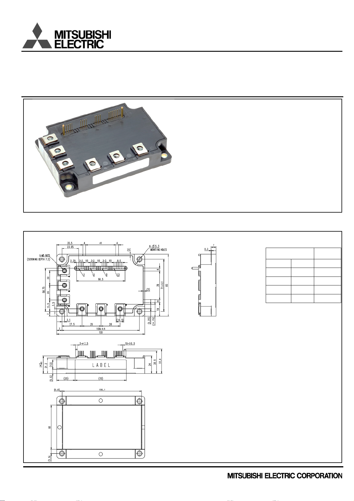
<Intelligent Power Modules>
PM100RG1C120
FLAT-BASE TYPE
INSULATED PACKAGE
APPLICATION
General purpose inverter, servo drives and other motor controls
PACKAGE OUTLINES Dimensions in mm
FEATURE
a) Adopting Full-Gate CSTBTTM chip.
b) The over-temperature protection which
detects the chip surface temperature of
CSTBT
TM
is adopted.
c) Error output signal is available from
each protection upper and lower arm of IPM.
d) Outputting an error signal corresponding
to the abnormal state (error mode identification)
UL Recognized under UL1557, File No. E323585
This product is compliant with the Restriction of the Use of Certain
Hazardous Substances in Electrical and Electronic Equipment
(RoHS) directive 2011/65/EU.
Tolerance otherwise specified
Division of
Dimension
0.5 to 3 ±0.2
over 3 to 6 ±0.3
over 6 to 30 ±0.5
over 30 to 120 ±0.8
over 120 to 400 ±1.2
TERMINAL CODE
1.V
UPC
2.U
FO
3.U
P
4.V
UP1
5.V
VPC
6.V
FO
7.V
P
8.V
VP1
9.V
WPC
10.W
FO
11. W
P
WP1
NC
N1
N
N
O
12.V
13.V
14.V
15.BR
16.UN
17.V
18.W
19.F
Tolerance
APPLICATION NOTE <CMH-11642-A>
Publication date : Nov, 2017
1
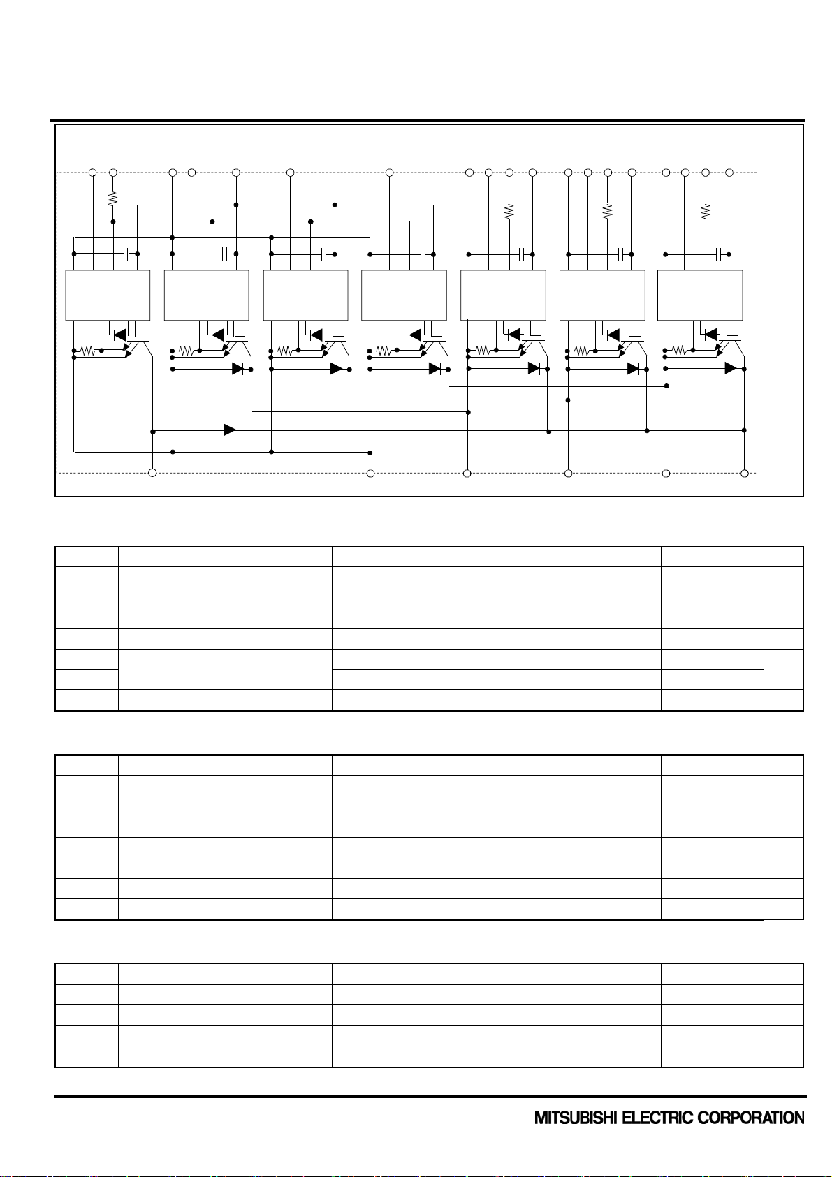
<Intelligent Power Modules>
PM100RG1C120
HIGH POWER SWITCHING USE
INSULATED TYPE
INTERNAL FUNCTIONS BLOCK DIAGRAM
UPC
V
UPC
WPC
GND
, V
, VP-V
, VFO-V
W
P
W
INGND
Si
VP1-VVPC
VPC
VPC
V
Fo
1.5k
Fo
OT
, V
, WP-V
, WFO-V
V
P
V
WP1
V
VPC
IN
GND
Vcc
GND Si OT
OUT
WP1-VWPC
, VN1-VNC 20 V
, UN, VN, WN, Br -VNC 20 V
WPC
, Fo-VNC 20 V
WPC
VP1
V
Fo
1.5k
VccFo
OUT
U
P
V
UPC
U
Fo
1.5k
GND
FoIN
GNDSiOT OUT
V
UP1
Vcc
PUVWN
A
A
A
Fo V
Br
1.5k
NCWN
V
N1
V
N
U
N
FoIN
GND
GND Si OT OUT
Vcc
GND
FoIN
Vcc
GND Si OT OUT
VccFoINGND
GND Si OT OUT
GND
GND Si OT OU T
Vcc
FoIN
MAXIMUM RATINGS (Tvj = 25°C, unless otherwise noted)
INVERTER PART
Symbol Parameter Conditions Ratings Unit
V
Collector-Emitter Voltage VD=15 V, V
CES
IC
I
Pulse 200
CRM
P
Total Power Dissipation TC=25 °C 735 W
tot
IE Emitter Current TC=25 °C 100
I
(Free-wheeling Diode Forward current) Pulse 200
ERM
Tv j Junction Temperature -20 ~ +150 °C
*: Tc measurement point is just under the chip.
BRAKE PART
Symbol Parameter Conditions Ratings Unit
V
Collector-Emitter Voltage VD=15 V, V
CES
IC
I
Pulse 100
CRM
P
Total Power Dissipation TC=25 °C 480 W
tot
V
Diode Rated Reverse DC Voltage TC=25 °C 1200 V
R(DC)
IF Diode Forward Current TC=25 °C 50 A
Tj Junction Temperature -20 ~ +150 °C
*: Tc measurement point is just under the chip.
CONTROL PART
Symbol Parameter Conditions Ratings Unit
VD Supply Voltage Applied between: V
V
Input Voltage Applied between: UP-V
CIN
VFO Fault Output Supply Voltage Applied between: UFO-V
IFO Fault Output Current Sink current at UFO, VFO, WFO, Fo terminals 20 mA
B
Collector Current
Collector Current
=15 V 1200 V
CIN
TC=25 °C 100
=15 V 1200 V
CIN
TC=25 °C 50
UP1-VUPC
APPLICATION NOTE <CMH-11642-A>
2
<Intelligent Power Modules>
PM100RG1C120
HIGH POWER SWITCHING USE
INSULATED TYPE
TOTAL SYSTEM
Symbol Parameter Conditions Ratings Unit
V
Supply Voltage Protected by SC VD =13.5 V~16.5 V, Inverter Part, Tvj=+125°C start 800 V
CC(PROT)
T
Storage Temperature - -40 ~ +125 °C
stg
TC Operating Case Temperature - -20 ~ +125 °C
V
Isolation Voltage 60Hz, Sinusoidal, Charged part to Base plate, AC 1min, RMS 2500 V
isol
*: Tc measurement point is just under the chip.
THERMAL RESISTANCE
Symbol Parameter Conditions
R
th(j-c)Q
R
Inverter, Junction to case, FWD, per 1 element (Note1) - - 0.25
th(j-c)D
R
th(j-c)Q
R
th(j-c)D
R
th(c-s)
Note1. If you use this value, R
Thermal Resistance
Brake, Junction to case, IGBT, per 1 element (Note1) - - 0.26
Brake, Junction to case, FWD, per 1 element (Note1) - - 0.41
Contact Thermal Resistance
should be measured just under the chips.
th(s-a)
Note2. Typical value is measured by using thermally conductive grease of λ=0.9W/(m·K), D
Inverter, Junction to case, IGBT, per 1 element (Note1) - - 0.17
Case to heat sink, per 1 module,
Thermal grease applied (Note.1, 2)
=50 μm.
(C-S)
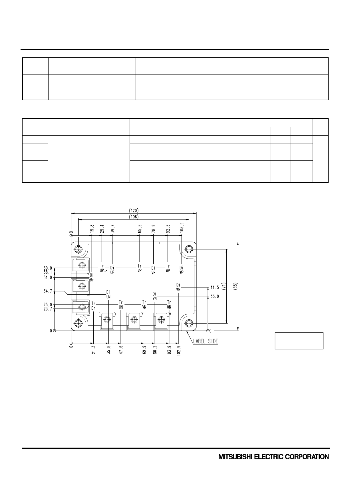
CHIP LOCATION (Top view) Dimension in mm, torelance: ±1mm
Limits
Min. Typ. Max.
- 8.4 - K/kW
Tr** : IGBT
Di** : FWD
Unit
K/W
APPLICATION NOTE <CMH-11642-A>
3
<Intelligent Power Modules>
PM100RG1C120
HIGH POWER SWITCHING USE
INSULATED TYPE
ELECTRICAL CHARACTERISTICS (Tv j= 25°C, unless otherwise noted)
INVERTER PART
Symbol Parameter Conditions
V
=15 V, IC=100 A Tv j=25 °C
D
V
Collector-Emitter Saturation Voltage
CEsa t
V
=0 V, Pulsed, (Fig.1) Tv j =125 °C
CIN
=15 V, IE=100 A, Tv j=25 °C
V
D
VEC Emitter-Collector Voltage
V
= 15 V, pulsed, (Fig.2) Tv j =125 °C
CIN
ton
trr V
t
Tv j=125 °C, - 0.2 0.4
c(on)
t
Inductive Load - 1.2 2.8
off
t
c(off)
I
Collector-Emitter Cut-off Current
CES
Switching Time
(Fig.3, 4) - 0.4 1.2
VD=15 V, V
=600 V, I
CC
V
V
, VD=15 V,
CE=VCES
=15 V (Fig.5)
CIN
=0 V←→15 V, 0.3 0.8 1.2
CIN
=100A, - 0.2 0.4
C
Terminal - - 1.85
Chip - 1.3 -
Terminal - - 2.1
Chip - 1.5 -
Terminal - - 2.4
Chip - 1.75 -
Terminal - - 2.65
Chip - 1.95 -
Tv j =25 °C - - 1
Tv j =125 °C - - 10
Limits
Min. Typ. Max.
Unit
V
V
μs
mA
BRAKE PART
Symbol Parameter Conditions
=15 V, IC=50A Tv j=25 °C
V
D
V
Collector-Emitter Saturation Voltage
CEsa t
V
=0 V, Pulsed, (Fig.1) Tv j =125 °C
CIN
VFM Diode Forward Voltage IF=50A
I
Collector-Emitter Cut-off Current VCE=V
CES
, VD=15 V, V
CES
=15 V (Fig.5)
CIN
Tv j =25 °C
Tv j =125 °C
Limits
Min. Typ. Max.
Unit
Terminal - - 1.75
Chip - 1.3 -
Terminal - - 2.0
V
Chip - 1.5 -
Terminal - - 2.35
Chip - 1.75 -
Terminal - - 2.6
V
Chip - 1.95 -
Tv j =25 °C - - 1
Tv j =125 °C - - 10
mA
APPLICATION NOTE <CMH-11642-A>
4

<Intelligent Power Modules>
PM100RG1C120
HIGH POWER SWITCHING USE
INSULATED TYPE
ELECTRICAL CHARACTERISTICS (Tvj = 25°C, unless otherwise noted)
CONTROL PART
Symbol Parameter Conditions
V
- 4 6
P1-VPC
VN1-VNC - 16 24
ID Circuit Current
=15 V, V
V
D
VD=15 V, V
=15 V
CIN
=0 V←→15 V, VCC=800 V VP1-VPC - 29 35
CIN
IC=0A, Tv j=125 °C, fC≤20kHz VN1-VNC - 103 120
V
Input ON Threshold Voltage Applied between: 1.2 1.5 1.8
th(ON)
V
Input OFF Threshold Voltage UP-V
th(OFF)
SC Short Circuit Trip Level -20≤Tvj≤125 °C, VD=15 V (Fig.3, 6)
t
Short Circuit Current Delay Time VD=15 V, Tv j=125 °C (Fig.3, 6) - 2.0 - μs
d(SC)
OT
OT
(hys)
Over Temperature Protection Detect temperature of IGBT chip surface
Hysteresis - 20 -
UVt Supply Circuit
UVr Under-Voltage Protection Reset level - 12.5 -
I
FO(H)
I
FO(L)
Fault Output Current V
- 10 15
UPC
, VP-V
VPC
, WP-V
WPC
-
=15 V, VFO=15 V (Note3)
D
, UN, VN, WN, Br-VNC 1.7 2.0 2.3
Inverter 200 - -
Brake 100 - -
Trip level 150 - -
Trip level 11.0 12.0 12.7
OT
tFO Fault Output Pulse Width VD=15 V (Note3)
UV
SC
Note3. Fault output is given only when the internal SC, OT & UV protections schemes of either upper or lower arm device operate to protect it.
Limits
Min. Typ. Max.
- - 0.01
-
8.0
-
4.0
-
2.0
Unit
mA
V
A
°C
V
mA
-
ms
-
MECHANICAL RATINGS AND CHARACTERISTICS
Symbol Parameter Conditions
Ms Mounting Torque Mounting part screw : M5 2.5 3.0 3.5
Mt Mounting Torque Main terminal part screw : M5 2.5 3.0 3.5
m mass - - 425 - g
Limits
Min. Typ. Max.
Unit
N•m
RECOMMENDED CONDITIONS FOR USE
Symbol Parameter Conditions Recommended value Unit
VCC Supply Voltage Applied across P-N terminals ≤ 800 V
VD Control Supply Voltage
V
Input ON Voltage Applied between : ≤ 0.8
CIN(ON)
V
Input OFF Voltage UP-V
CIN(OFF)
f
PWM Input Frequency Using Application Circuit of Fig. 8 ≤ 20 kHz
PWM
t
Arm Shoot-through Blocking Time For IPM’s each input signals (Fig.7) ≥ 2.5 μs
dead
This product is compliant with the Restriction of the Use of Certain Hazardous Substances in Electrical and Electronic
Equipment (RoHS) directive 2011/65/EU.
Note4. With ripple satisfying the following conditions: dv/dt swing ≤ ±5 V/μs, Variation ≤ 2 V peak to peak
Applied between :
V
UP1-VUPC
UPC
, V
, VP-V
VP1-VVPC
VPC
, V
WP1-VWPC,VN1-VNC
, WP-V
WPC
(Note4)
15.0±1.5
, UN, VN, WN, Br-VNC ≥ 9.0
V
V
APPLICATION NOTE <CMH-11642-A>
5

<Intelligent Power Modules>
PM100RG1C120
HIGH POWER SWITCHING USE
INSULATED TYPE
PRECAUTIONS FOR TESTING
1. Before applying any control supply voltage (V
supply voltage and each input signal should be kept off state.
After this, the specified ON and OFF level setting for each input signal should be done.
2. When performing “SC” tests, the turn-off surge voltage spike at the corresponding protection operation should not be allowed to
rise above V
rating of the device.
CES
(These test should not be done by using a curve tracer or its equivalent.)
Vcc
Fo
VD(all)
Fo
Vcin
IN
GND
), the input terminals should be pulled up by resistors, etc. to their corresponding
D
P,(U,V,W,B)
V
Vcc
Fo
Ic
VD(all)
Fo
Vcin
IN
GND
P,(U,V ,W,B)
V
I
E
VD(all)
VD(all)
U,V,W,B(N)
Vcin
Vcin
Fig.1 V
P
Vcc
Fo
Fo
IN
GND
Vcc
Fo
Fo
IN
GND
U,V,W
V
N
Tes t Fig.2 VEC Test
CEsat
Vcc
Fo
Vcin
Fo
Vcin
Fo
IN
GND
Vcc
Fo
IN
GND
V
I
C
VD(all)
CC
VD(all)
Fig.3 Switching time and SC test circuit Fig.4 Switching time test waveform
P
V
V
U,V, W
N
CC
I
C
VD(all)
Fo
Vcin
Vcc
Fo
IN
GND
P,(U,V ,W,B)
A
pulse
V
CE
Fig.5 I
U,V,W,B(N)
Tes t Fig.6 SC test waveform
CES
U,V,W,B(N)
APPLICATION NOTE <CMH-11642-A>
Fig. 7 Dead time measurement point example
6

<Intelligent Power Modules>
PM100RG1C120
HIGH POWER SWITCHING USE
INSULATED TYPE
20k ≥10µ
VUP1
≥10µ
≥10µ
UFO
UP
VUPC
VVP1
VFO
VP
VVPC
VWP1
WFO
WP
VWPC
UN
VN
VN1
WN
VNC
VN1
Br
Fo
VD
VD
VD
VD
IF
≥0.1µ
20k
IF
≥0.1µ
20k ≥10µ
IF
≥0.1µ
20k ≥10µ
IF
≥0.1µ
IF
5V
20k
≥0.1µ
1k
1.5k
1.5k
1.5k
1.5k
Vcc
Fo
IN
GND
Vcc
Fo
IN
GND
Vcc
Fo
IN
GND
Vcc
Fo
IN
GND
Vcc
Fo
IN
GND
Vcc
Fo
IN
GND
Vcc
Fo
IN
GND
OUT
OT
Si
GND
OUT
OT
Si
GND
OUT
OT
Si
GND
OUT
OT
Si
GND
OUT
OT
Si
GND
OUT
OT
Si
GND
OUT
OT
Si
GND
P
+
-
U
V
W
N
B
M
: Interface which is the same as the U-phase
Fig. 8 Application Example Circuit
NOTES FOR STABLE AND SAFE OPERATION ;
• Design the PCB pattern to minimize wiring length between opto-coupler and IPM’s input terminal, and also to minimize the stray capacity
between the input and output wirings of opto-coupler.
• Connect low impedance capacitor between the Vcc and GND terminal of each fast switching opto-coupler.
• Fast switching opto-couplers: t
PLH
, t
≤ 0.8μs, Use High CMR type.
PHL
• Slow switching opto-coupler: CTR > 100% (*can be applied to Brake part input signal, in this case, resistor should be selected properly).
• Use 4 isolated control power supplies (V
). Also, care should be taken to minimize the instantaneous voltage charge of the power supply.
D
• Make inductance of DC bus line as small as possible, and minimize surge voltage using snubber capacitor between P and N terminal.
APPLICATION NOTE <CMH-11642-A>
7

<Intelligent Power Modules>
Y
PM100RG1C120
HIGH POWER SWITCHING USE
INSULATED TYPE
PERFORMANCE CURVES
Inverter part
COLLECTOR-EMITTER SATURATION
VOLTAGE (VS. Ic) CHARACTERISTICS
120
(A)
C
COLLECTOR CURRENT I
100
VD=15V, Chip
80
60
40
20
0
0.00.51.01.5
(TYPICAL)
Tvj=25°C
Tvj=125°C
COLLECTOR-EMITTER SATURATION
VOLTAGE VCEsat (V)
SWITCHING TIME (t
CHARACTERISTICS
10.0
1.0
Vcc=600V
V
=15V
D
Inductive Load
(TYPICAL)
Tvj=25°C
Tvj=125°C
SWITCHING TIME (μs)
0.1
0 20406080100120
COLLECTOR CURRENT I
SWITCHING ENERGY CHARACTERISTICS
10.0
Vcc=600V
9.0
V
=15V
D
8.0
7.0
Inductive Load
6.0
5.0
4.0
3.0
2.0
1.0
SWITCHING ENERGY Eon (mJ/pulse)
0.0
0 20406080100120
(TYPICAL)
Tvj=25°C
Tvj=125°C
COLLECTOR CURRENT I
FREE WHEELING DIODE FORWARD
CHARACTERISTICS
120
VD=15V, Chip
100
(A)
E
80
EMITTER - COLLECTOR VOLTAGE VEC (V)
, t
)
on
off
60
40
EMITTER CURRENT I
20
0
0.0 0. 5 1.0 1.5 2.0
SWITCHING TIME (t
(TYPICAL)
Tvj=25°C
Tvj=125°C
c(on)
, t
c(off)
)
CHARACTERISTICS
1
t
c(off)
(TYPICAL)
t
off
t
on
(A)
C
0.1
SWITCHING TIME (μs)
0.01
0 20406080100120
COLLECTOR CURRENT IC (A)
FREE WHEELING DIODE REVERSE RECOVER
t
c(on)
Vcc=600V
V
=15V
D
Tvj=25°C
Tvj=125°C
Inductive Load
ENERGY CHARACTERISTICS
C
(A)
Eon
E
20.0
18.0
16.0
14.0
12.0
10.0
8.0
6.0
off
4.0
2.0
0.0
6.0
Vcc=600V
V
=15V
D
5.0
Inductive Load
4.0
3.0
2.0
SWITCHING ENERGY Eoff (mJ)
1.0
0.0
REVERSE RECOVERY ENERGY (mJ/pulse)
0 20406080100120
(TYPICAL)
Tvj=25°C
Tvj=125°C
EMITTER CURRENT IE (A)
APPLICATION NOTE <CMH-11642-A>
8

<Intelligent Power Modules>
PM100RG1C120
HIGH POWER SWITCHING USE
INSULATED TYPE
REVERSE RECOVERY TIME (ns)
REVERSE RECOVERY CURRENT (A)
UVt / UVr (V)
FREE WHEELING DIODE REVERSE
RECOVERY CHARACTERISTICS
t
rr
I
rr
(TYPICAL)
1000
100
10
1
0 20 40 60 80 100 120
EMITTER CURRENT I
UV TRIP LEVEL VS. Tvj CHARACTERISTICS
20
18
16
14
12
10
8
6
4
2
0
-50 0 50 100 150
(TYPICAL)
Tvj (°C) *inverter and brake part
TRANSIENT THERMAL IMPEDANCE
CHARACTERISTICS
(TYPICAL)
Vcc=600V
V
=15V
D
Tvj=25°C
Tvj=125°C
Inductive Load
(A)
E
UV
UV
VS. fC CHARACTERISTICS
I
140
120
100
80
(mA)
60
D
I
40
20
SC TRIP LEVEL VS. Tvj CHARACTERISTICS
2.0
1.8
1.6
r
t
1.4
1.2
1.0
SC
0.8
0.6
0.4
(SC of Tvj=25°C is normalized 1)
0.2
0.0
D
(TYPICAL, MAXIMUM)
Vcc=800V
V
=15V, Tvj=125°C
D
TYPICAL
MAXIMUM
0
0 5 10 15 20 25
N side
P side
fc (kHz) *inverter and brake part
(TYPICAL)
VD=15V
-50 0 50 100 150
Tvj (°C) *inverter and brake part
10
1
Zth(j-c)
0.1
0.01
0.001
NORMARIZED TRANSIENT THERMAL IMPEDANCE
0.00001 0.0001 0.001 0.01 0.1 1 10
Single Pulse
IGBT Part;
Per unit base: Rth(j-c)Q=0.17K /W
FWD Part;
Per unit base: Rth(j-c)D=0.25K /W
TIME (s)
APPLICATION NOTE <CMH-11642-A>
9

<Intelligent Power Modules>
PM100RG1C120
HIGH POWER SWITCHING USE
INSULATED TYPE
PERFORMANCE CURVES
Brake part
COLLECTOR-EMITTER SATURATION
VOLTAGE (VS. Ic) CHARACTERISTICS
60
(A)
C
COLLECTOR CURRENT I
VD=15V, Chip
50
40
30
20
10
0
0.0 0.5 1.0 1.5
(TYPICAL)
Tvj=25°C
Tvj=125°C
COLLECTOR-EMITTER SATURATION
VOLTAGE VCEsat (V)
TRANSIENT THERMAL IMPEDANCE
CHARACTERISTICS
(TYPICAL)
FREE WHEELING DIODE FORWARD
CHARACTERISTICS
60
VD=15V, Chip
50
(A)
E
40
30
20
EMITTER CURRENT I
10
0
0.0 0.5 1.0 1.5 2.0
EMITTER - COLLECTOR VOLTAGE VEC (V)
(TYPICAL)
Tvj=25°C
Tvj=125°C
10
1
Zth(j-c)
0.1
0.01
0.001
NORMARIZED TRANSIENT THERMAL IMPEDANCE
0.00001 0.0001 0.001 0.01 0.1 1 10
Single Pulse
IGBT Part;
Per unit base: Rth(j-c)Q=0.26K /W
FWD Part;
Per unit base: Rth(j-c)D=0.41K /W
TIME (s)
APPLICATION NOTE <CMH-11642-A>
10
<Intelligent Power Modules>
PM100RG1C120
HIGH POWER SWITCHING USE
INSULATED TYPE
Keep safety first in your circuit designs!
This product is designed for industrial application purpose. The performance, the quality and support level of the product is
guaranteed by “Customer's Std. Spec.”.
Mitsubishi Electric Corporation puts its reasonable effort into making semiconductor products better and more reliable, but there
is always the possibility that trouble may occur with them by the reliability lifetime such as Power Cycle, Thermal Cycle or others,
or to be used under special circumstances(e.g. high humidity, dusty, salty, highlands, environment with lots of organic matter /
corrosive gas / explosive gas, or situation which terminal of semiconductor products is received strong mechanical stress).
In the customer's research and development, please evaluate it not only with a single semiconductor product but also in the
entire system, and judge whether it's applicable. Furthermore, trouble with semiconductors may lead to personal injury, fire or
property damage. Remember to give due consideration to safety when making your circuit designs, with appropriate measures
such as (i) placement of substitutive, auxiliary circuits (e.g. appropriate fuse or circuit breaker between a power supply and
semiconductor products), (ii) use of non-flammable material or (iii) prevention against any malfunction or mishap.
Notes regarding these materials
•These materials are intended as a reference to assist our customers in the selection of the Mitsubishi semiconductor product
best suited to the customer's application; they do not convey any license under any intellectual property rights, or any other
rights, belonging to Mitsubishi Electric Corporation or a third party.
•Mitsubishi Electric Corporation assumes no responsibility for any damage, or infringement of any third-party's rights, originating
in the use of any product data, diagrams, charts, or circuit application examples contained in these materials.
•All information contained in these materials, including product data, diagrams and charts represents information on products at
the time of publication of these materials, and are subject to change by Mitsubishi Electric Corporation without notice due to
product improvements or other reasons. It is therefore recommended that customers contact Mitsubishi Electric Corporation or
an authorized Mitsubishi Semiconductor product distributor for the latest product information before purchasing a product listed
herein.
The information described here may contain technical inaccuracies or typographical errors. Mitsubishi Electric Corporation
assumes no responsibility for any damage, liability, or other loss rising from these inaccuracies or errors.
Please also pay attention to information published by Mitsubishi Electric Corporation by various means, including the Mitsubishi
Semiconductor home page (www.MitsubishiElectric.com/semiconductors/).
•When using any or all of the information contained in these materials, including product data, diagrams, and charts, please be
sure to evaluate all information as a total system before making a final decision on the applicability of the information and
products. Mitsubishi Electric Corporation assumes no responsibility for any damage, liability or other loss resulting from the
information contained herein.
•Mitsubishi Electric Corporation semiconductors are not designed or manufactured for use in a device or system that is used
under circumstances in which human life is potentially at stake. Therefore, this product should not be used in such applications.
Please contact Mitsubishi Electric Corporation or an authorized Mitsubishi Semiconductor product distributor when considering
the use of a product contained herein for any specific purposes, such as apparatus or systems for transportation, vehicular,
medical, aerospace, nuclear, or undersea repeater use.
•In the case of new requirement is available, this material will be revised upon consultation.
•The prior written approval of Mitsubishi Electric Corporation is necessary to reprint or reproduce in whole or in part these
materials.
•If these products or technologies are subject to the Japanese export control restrictions, they must be exported under a license
from the Japanese government and cannot be imported into a country other than the approved destination.
Any diversion or re-export contrary to the export control laws and regulations of Japan and/or the country of destination is
prohibited.
•Please contact Mitsubishi Electric Corporation or an authorized Mitsubishi Semiconductor product distributor for further details
on these materials or the products contained therein.
Generally the listed company name and the brand name are the trademarks or registered trademarks of the respective companies.
Note:
The characteristics curves are presented for reference only and not guaranteed by production test,
unless otherwise noted.
© 2018 MITSUBISHI ELECTRIC CORPORATION. ALL RIGHTS RESERVED.
APPLICATION NOTE <CMH-11642-A>
11
 Loading...