

Mitsubishi Electric US, Inc PM100CG1A065, PM100CG1AL065 Data Sheet
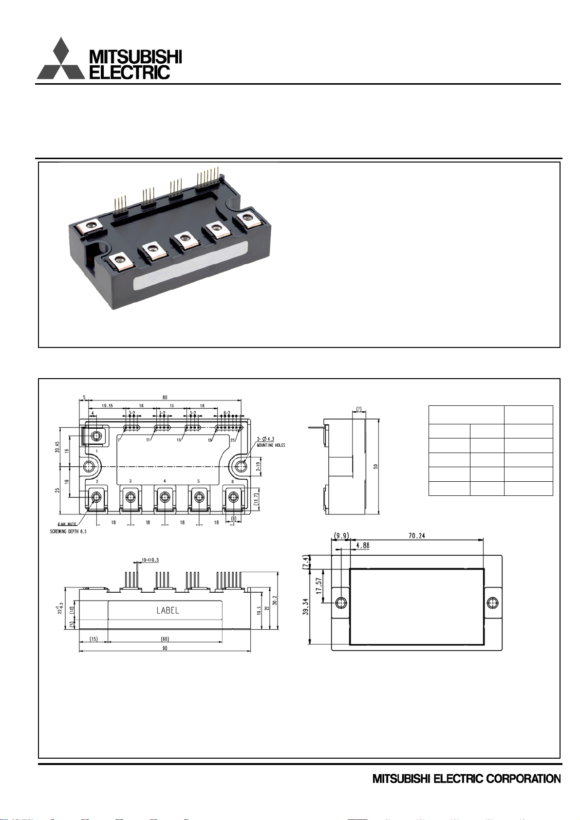
<Intelligent Power Modules>
PM100CG1A065/PM100CG1AL065
FLAT-BASE TYPE
INSULATED PACKAGE
APPLICATION
General purpose inverter, servo drives and other motor controls
PACKAGE OUTLINES Dimensions in mm
TERMINAL CODE
----CG1A type----
1.NC, 2.P, 3.N, 4.U, 5.V, 6.W, 7.V
15.V
, 16.WFO, 17.WP, 18.V
WPC
, 19.VNC, 20.VN1, 21.NC, 22.UN, 23.VN, 24.WN, 25.FO
WP1
----CG1AL type----
1.N, 2.P, 3.NC, 4.U, 5.V, 6.W, 7.V
15.V
, 16.WFO, 17.WP, 18.V
WPC
, 19.VNC, 20.VN1, 21.NC, 22.UN, 23.VN, 24.WN, 25.FO
WP1
, 8.UFO, 9.UP, 10.V
UPC
, 8.UFO, 9.UP, 10.V
UPC
FEATURE
a) Adopting Full-Gate CSTBTTM chip.
b) The over-temperature protection which
detects the chip surface temperature of
CSTBT
TM
is adopted.
c) Error output signal is available from
each protection upper and lower arm of IPM.
d) Outputting an error signal corresponding
to the abnormal state (error mode identification)
UL Recognized under UL1557, File No. E323585
This product is compliant with the Restriction of the Use of Certain
Hazardous Substances in Electrical and Electronic Equipment
(RoHS) directive 2011/65/EU.
UP1
UP1
, 11.V
, 11.V
, 12.VFO, 13.VP, 14.V
VPC
, 12.VFO, 13.VP, 14.V
VPC
Tolerance otherwise specified
Division of
Dimension
0.5 to 3 ±0.2
over 3 to 6 ±0.3
over 6 to 30 ±0.5
over 30 to 120 ±0.8
over 120 to 400 ±1.2
,
VP1
,
VP1
Tolerance
APPLICATION NOTE <CMH-11599-A>
Publication date : Nov, 2017
1
<Intelligent Power Modules>
PM100CG1A065/PM100CG1AL065
HIGH POWER SWITCHING USE
INSULATED TYPE
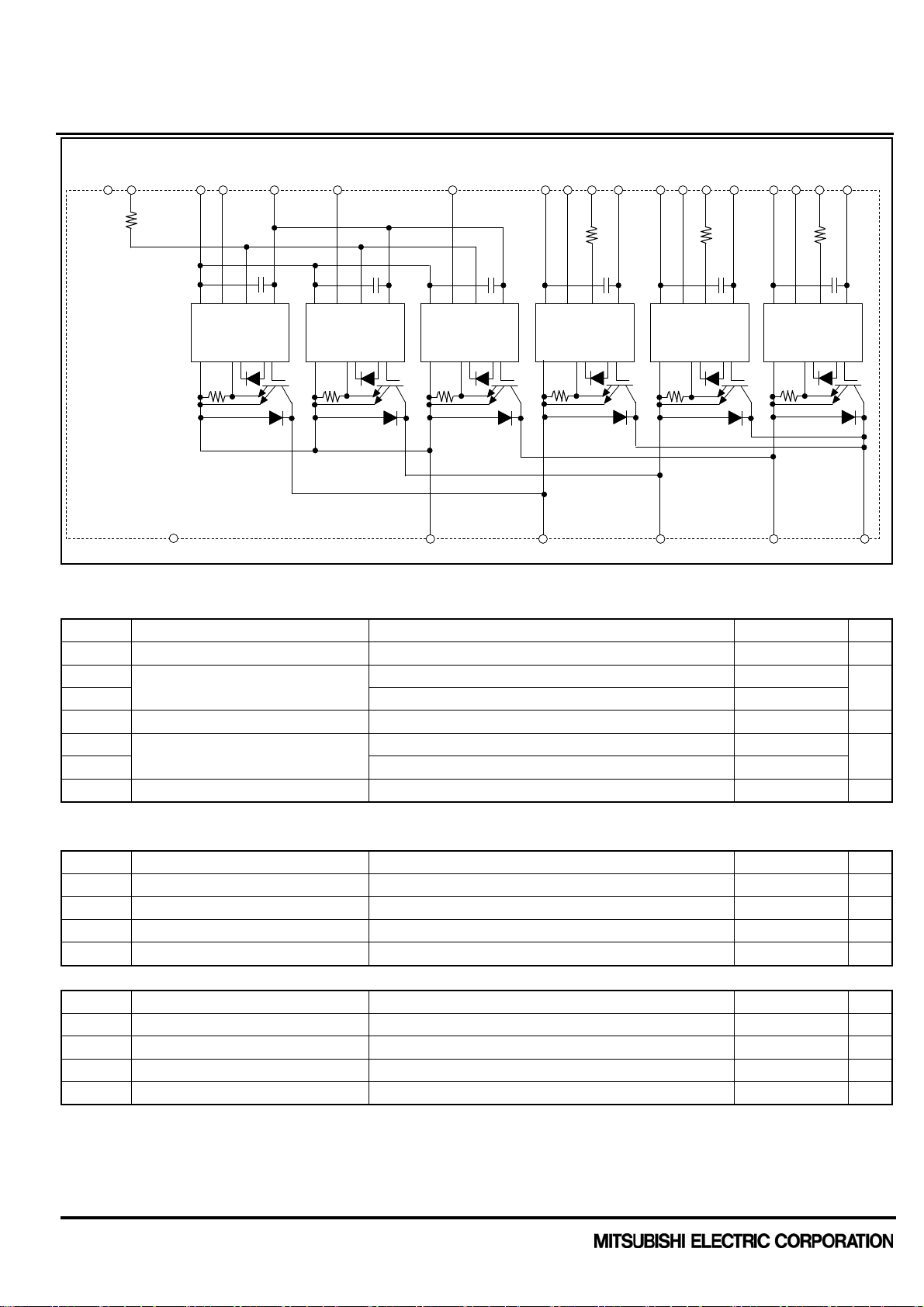
INTERNAL FUNCTIONS BLOCK DIAGRAM
NC Fo
V
NCWN
V
N1
V
N
V
U
N
V
W
WPC
WP1
P
W
Fo
V
V
VPC
V
P
VP1
V
Fo
U
V
UPC
V
P
UP1
U
Fo
1.5k
FoIN
GND
GND
NC
Vcc
Si OT OUT
GND
VccFoINGND
Si OT OUT
GND
VccFoINGND
Si OT OUT
GND Si OT OUT
1.5k
Fo
INGND
Vcc
GND
GND
1.5k
IN
Si OT OUT
VccFo
GND
1.5k
VccFoINGND
Si OT OUT
PUVWN
MAXIMUM RATINGS (Tvj = 25°C, unless otherwise noted)
INVERTER PART
Symbol Parameter Conditions Ratings Unit
V
Collector-Emitter Voltage VD=15 V, V
CES
IC
I
Pulse 200
CRM
P
Total Power Dissipation TC=25 °C 357 W
tot
Collector Current
TC=25 °C 100
IE Emitter Current TC=25 °C 100
I
(Free-wheeling Diode Forward current) Pulse 200
ERM
Tv j Junction Temperature -20 ~ +150 °C
=15 V 650 V
CIN
A
A
*: Tc measurement point is just under the chip.
CONTROL PART
Symbol Parameter Conditions Ratings Unit
VD Supply Voltage Applied between: V
V
Input Voltage Applied between: UP-V
CIN
VFO Fault Output Supply Voltage Applied between: UFO-V
IFO Fault Output Current Sink current at UFO, VFO, WFO, Fo terminals 20 mA
UP1-VUPC
UPC
UPC
, V
, VP-V
, VFO-V
VP1-VVPC
, WP-V
VPC
VPC
, V
WP1-VWPC
, WFO-V
, VN1-VNC 20 V
, UN, VN, WN-VNC 20 V
WPC
, Fo-VNC 20 V
WPC
TOTAL SYSTEM
Symbol Parameter Conditions Ratings Unit
V
Supply Voltage Protected by SC VD =13.5 V~16.5 V, Inverter Part, Tvj=+125°C start 400 V
CC(PROT)
T
Storage Temperature - -40 ~ +125 °C
stg
TC Operating Case Temperature - -20 ~ +125 °C
V
Isolation Voltage 60Hz, Sinusoidal, Charged part to Base plate, AC 1min, RMS 2500 V
isol
*: Tc measurement point is just under the chip.
APPLICATION NOTE <CMH-11599-A>
2
<Intelligent Power Modules>
PM100CG1A065/PM100CG1AL065
HIGH POWER SWITCHING USE
INSULATED TYPE
THERMAL RESISTANCE
Symbol Parameter Conditions
R
th(j-c)Q
R
th(j-c)D
R
th(c-s)
Note1. If you use this value, R
Thermal Resistance
Junction to case, FWD, per 1 element (Note1) - - 0.56
Contact Thermal Resistance
should be measured just under the chips.
th(s-a)
Note2. Typical value is measured by using thermally conductive grease of λ=0.9W/(m·K), D
Junction to case, IGBT, per 1 element (Note1) - - 0.35
Case to heat sink, per 1 module,
Thermal grease applied (Note.1, 2)
=50 μm.
(C-S)
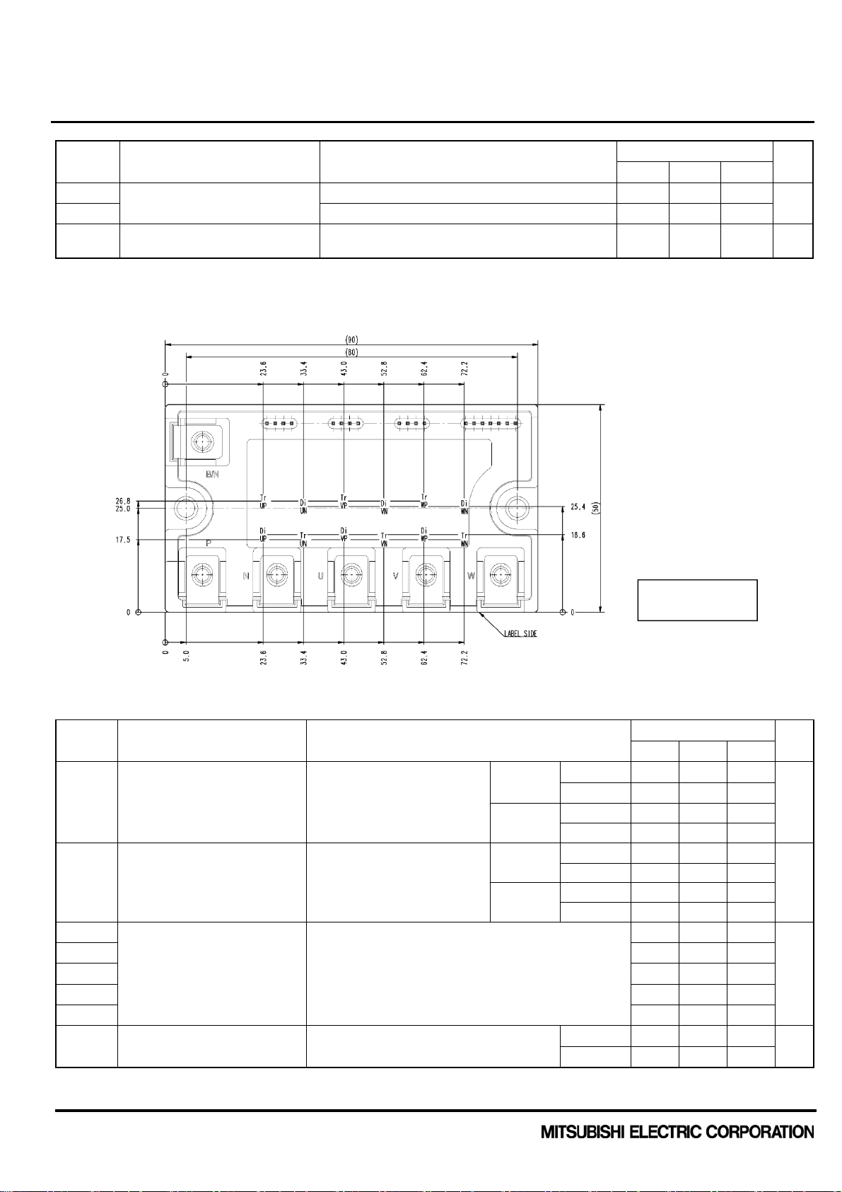
CHIP LOCATION (Top view) Dimension in mm, torelance: ±1mm
ELECTRICAL CHARACTERISTICS (Tvj= 25°C, unless otherwise noted)
INVERTER PART
Symbol Parameter Conditions
V
=15 V, IC=100 A Tv j=25 °C
D
V
Collector-Emitter Saturation Voltage
CEsa t
V
=0 V, Pulsed, (Fig.1) Tvj =125 °C
CIN
=15 V, IE=100 A, Tv j=25 °C
V
D
VEC Emitter-Collector Voltage
V
= 15 V, pulsed, (Fig.2) Tv j=125 °C
CIN
ton
trr V
t
Tv j=125 °C, - 0.17 0.75
c(on)
t
Inductive Load - 1.0 2.3
off
t
c(off)
I
Collector-Emitter Cut-off Current
CES
Switching Time
(Fig.3, 4) - 0.13 0.4
VD=15 V, V
=300 V, I
CC
V
V
, VD=15 V,
CE=VCES
=15 V (Fig.5)
CIN
=0 V←→15 V, 0.3 0.6 1.2
CIN
=100A, - 0.2 0.65
C
Terminal - - 1.75
Chip - 1.25 -
Terminal - - 2.0
Chip - 1.33 -
Terminal - - 1.95
Chip - 1.40 -
Terminal - - 2.05
Chip - 1.45 -
Tv j =25 °C - - 1
Tv j =125 °C - - 10
Limits
Min. Typ. Max.
- 19.1 - K/kW
Tr** : IGBT
Di** : FWD
Limits
Min. Typ. Max.
Unit
K/W
Unit
V
V
μs
mA
APPLICATION NOTE <CMH-11599-A>
3
 Loading...