FM400TU-2A
MITSUBISHI <MOSFET MODULE>
FM400TU-2A
HIGH POWER SWITCHING USE
INSULATED PACKAGE
●
ID(rms) .......................................................... 200A
● VDSS.............................................................100V
● Insulated Type
●
6-elements in a pack
●
Thermistor inside
●
UL Recognized
File No.E323585
APPLICATION
AC motor control of forklift (battery power source), UPS
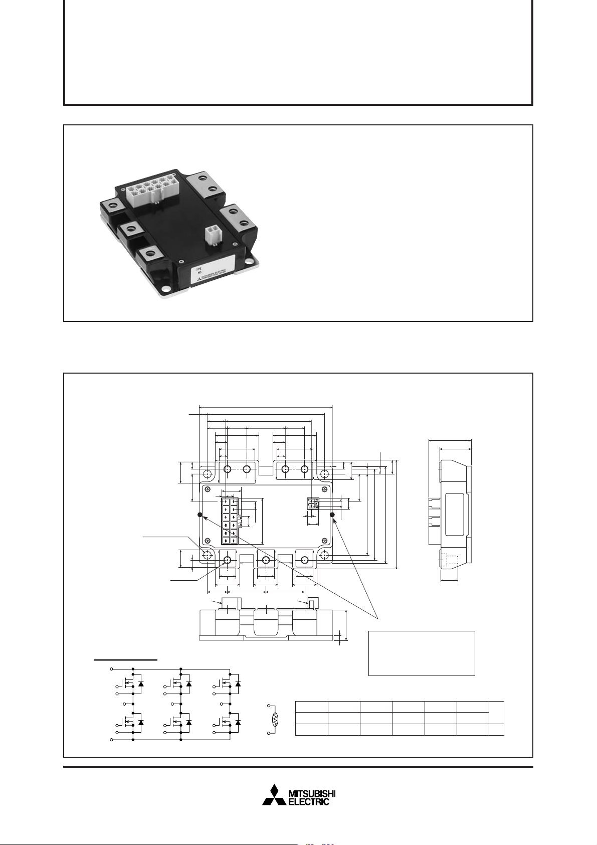
OUTLINE DRAWING & CIRCUIT DIAGRAM
110
±0.25
97
70.9
36
10
30
NP
13
14
5-6.5
38
9.2
UV
1414
32 3216.5
14
202020
B
3
(8.7)
(6)
3.96
W
4
MOUNTINGHOLES
CIRCUIT DIAGRAM
P
(17.5)
4-φ6.5
(14.5)
7-M6NUTS
6.5
(6)(6)
22.75
15.2
16.5
16 1632
36
10
30
7 7
(15.8)
6.5
3
7
1216
A
25
6.5
11.5
4
(14.5)
22.57
9.1
±0.25
90
80
75
67
Tc measured point
Housing Type of A and B
(Tyco Electronics P/N:)
A: 917353-1
B: 179838-1
Dimensions in mm
±1.0
35
+1.0
26
−0.5
LABEL
14
(SCREWING DEPTH)
(7)G
(1)S
(10)G
(4)S
U
P
U
P
U
N
U
N
N
(8)G
V
P
(2)SVP
UVW
V
(11)G
V
N
(5)S
(9)G
W
P
(3)S
W
P
N
(12)G
(6)S
W
N
W
N
(13)
(14)
(1)SUP
U
(7)G
(13)TH1
P
(2)S
V
P
V
P
(8)G
(14)TH2
(3)S
(9)G
(4)S
W
P
W
P
(10)G
(5)S
U
N
U
N
(11)G
V
N
V
N
(6)S
W
N
(12)GWN
A
B
Mar. 2013

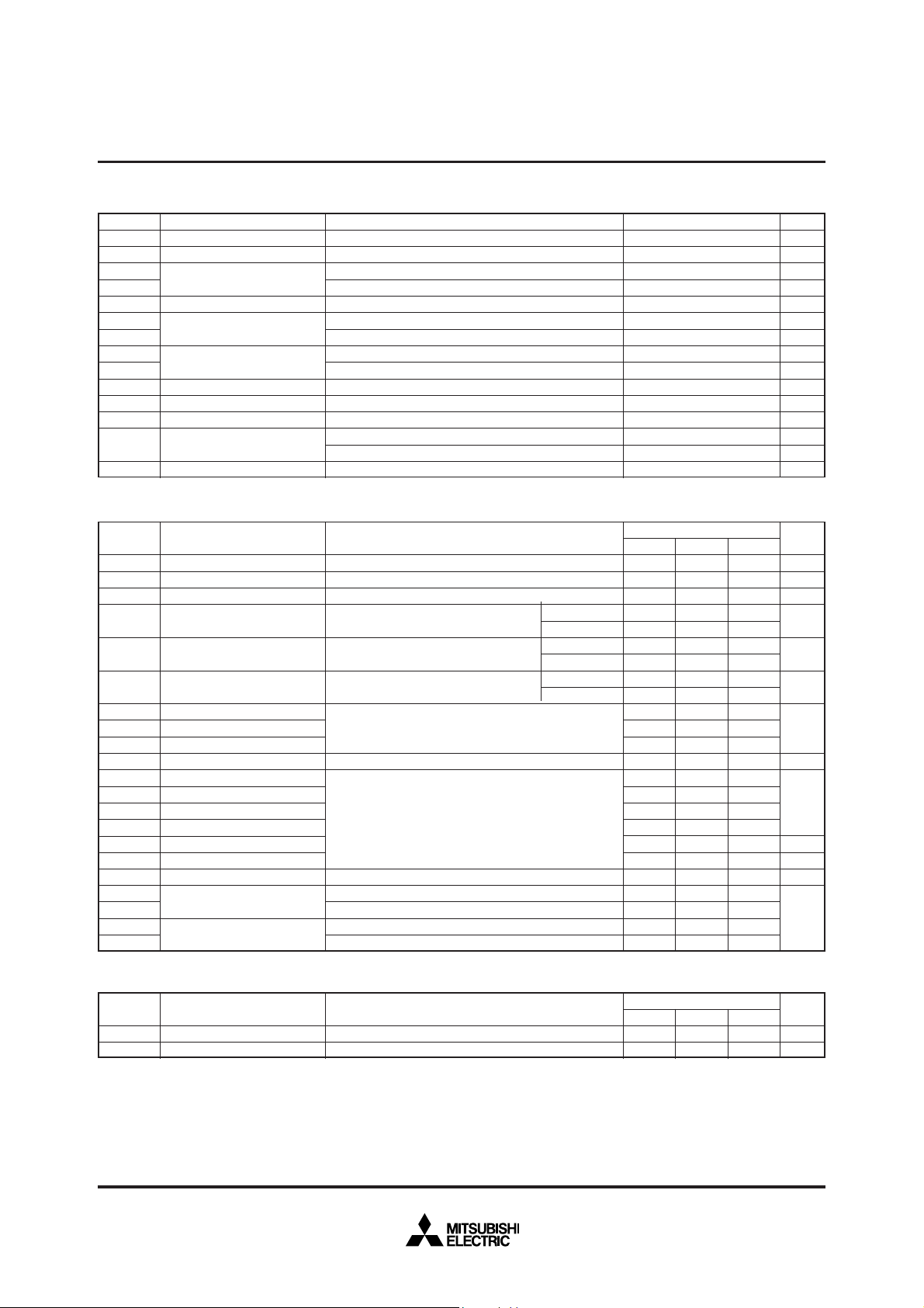
ABSOLUTE MAXIMUM RATINGS (Tj = 25°C unless otherwise specified.)
Symbol
V
DSS
VGSS
ID
IDM
IDA
1
IS*
ISM*
4
PD*
4
PD*
Tch
Tstg
Visol
—
—
Drain-source voltage
Gate-source voltage
Drain current
Avalanche current
Source current
1
Maximum power dissipation
Channel temperature
Storage temperature
Isolation voltage
Mounting torque
Weight
G-S Short
D-S Short
T
C’ = 130°C*
Pulse*
3
2
L = 10µH Pulse*
2
Pulse*
TC = 25°C
T
C’ = 25°C*
3
Main terminal to base plate, AC 1 min, f=60Hz, RMS
Main Terminal M6
Mounting to heat sink M6
Typical value
ConditionsItem
2
ELECTRICAL CHARACTERISTICS (Tj = 25°C unless otherwise specified.)
ConditionsItemSymbol
DSS
I
VGS(th)
IGSS
rDS(on)
(chip)
VDS(on)
(chip)
RDD'-SS'
Ciss
Coss
Crss
QG
td(on)
tr
td(off)
tf
1
trr*
1
Qrr*
1
VSD*
Rth(j-c)
Rth(j-c’)
Rth(c-s)
Rth(c’-s’)
Drain cutoff current
Gate-source threshold voltage
Gate leakage current
Static drain-source
On-state resistance
Static drain-source
On-state voltage
Internal lead resistance
Input capacitance
Output capacitance
Reverse transfer capacitance
Total gate charge
Turn-on delay time
Rise time
Turn-off delay time
Fall time
Reverse recovery time
Reverse recovery charge
Source-drain voltage
Thermal resistance
Contact thermal resistance
V
DS = VDSS, VGS = 0V
I
D = 20mA, VDS = 10V
V
GS = VGSS, VDS = 0V
I
D = 200A
V
GS = 15V
I
D = 200A
V
GS = 15V
I
D = 200A
terminal-chip
V
DS = 10V
V
GS = 0V
V
DD = 48V, ID = 200A, VGS = 15V
DD = 48V, ID = 200A, VGS1 = VGS2 = 15V
V
R
G = 6.3Ω, Inductive load switching operation
I
S = 200A
S = 200A, VGS = 0V
I
MOSFET part (1/6 module)*
MOSFET part (1/6 module)*
7
3
Case to fin, Thermal grease Applied*8 (1/6 module)
Case to fin, Thermal grease Applied*
Tj = 25°C
Tj = 125°C
Tj = 25°C
Tj = 125°C
Tj = 25°C
Tj = 125°C
3, *8
(1/6 module)
MITSUBISHI <MOSFET MODULE>
FM400TU-2A
HIGH POWER SWITCHING USE
INSULATED PACKAGE
Min.
—
4.7
—
—
—
—
—
—
—
—
—
—
—
—
—
—
—
—
—
—
—
—
—
—
Rating
100
±20
200
400
200
200
400
650
880
–40 ~ +150
–40 ~ +125
2500
3.5 ~ 4.5
3.5 ~ 4.5
600
Limits
Typ.
—
6
—
1.45
2.5
0.29
0.50
0.8
1.12
—
—
—
1200
—
—
—
—
—
6.0
—
—
—
0.1
0.09
Max.
0.40
400
400
450
300
250
0.19
0.142
7.3
1.5
2.0
—
—
—
—
75
10
—
—
1.3
—
—
Unit
V
V
A
A
A
A
A
W
W
°C
°C
V
N • m
N • m
g
Unit
1
mA
V
µA
mΩ
V
mΩ
nF
6
nC
ns
ns
µC
V
K/W
NTC THERMISTOR PART
Symbol
6
R25*
6
B*
1: It is characteristics of the anti-parallel, source to drain free-wheel diode (FWDi).
*
2: Pulse width and repetition rate should be such that the device junction temperature (Tj) does not exceed Tj max rating.
*
3: TC’ measured point is just under the chips. If use this value, Rth(s-a) should be measured just under the chips.
*
4: Pulse width and repetition rate should be such as to cause negligible temperature rise.
*
5: TTH is thermistor temperature.
*
6: B = (InR1-InR2)/(1/T1-1/T2) R1: Resistance at T1(K), R2: Resistance at T2(K)
*
7: TC measured point is shown in page OUTLINE DRAWING.
*
8: Typical value is measured by using thermally conductive grease of λ=0.9 W/(m·K).
*
Resistance
B Constant
TTH = 25°C*
Resistance at TTH = 25°C, 50°C*
5
ConditionsParameter
5
Min.
—
—
Limits
Typ.
100
4000
Max.
—
—
Unit
kΩ
K
Mar. 2013

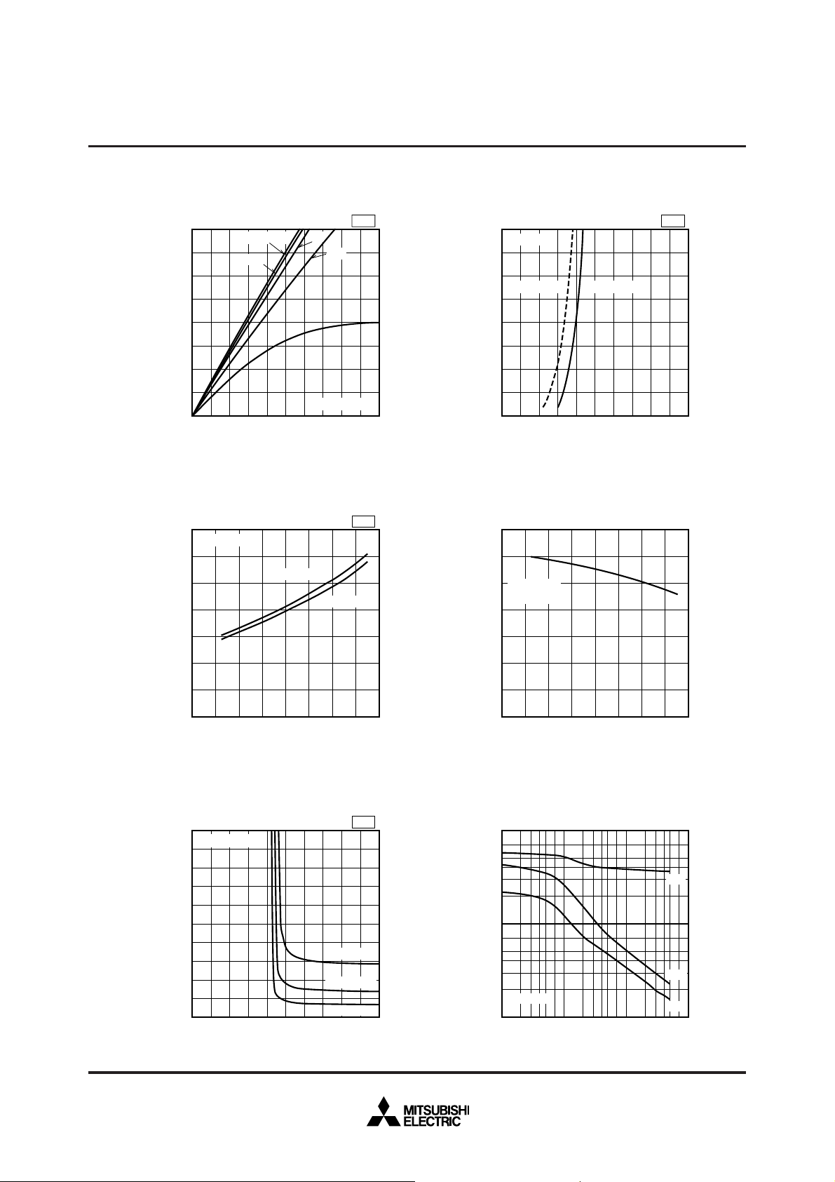
PERFORMANCE CURVES
MITSUBISHI <MOSFET MODULE>
FM400TU-2A
HIGH POWER SWITCHING USE
INSULATED PACKAGE
OUTPUT CHARACTERISTICS
(TYPICAL)
V
GS
= 20V
15V
12V
(A)
D
400
350
300
250
200
150
100
DRAIN CURRENT I
50
0
0 0.2 0.4 0.6 0.8 1.0
DRAIN-SOURCE VOLTAGE V
DRAIN-SOURCE ON-STATE
VOLTAGE VS. TEMPERATURE
3.5
ID = 200A
(mΩ)
3.0
DS(on)
2.5
(TYPICAL)
V
GS
= 12V
2.0
10V
Tj = 25°C
DS
V
GS
= 15V
Chip
(V)
Chip
9V
TRANSFER CHARACTERISTICS
(TYPICAL)
Tj = 25°C
(A)
D
400
300
V
DS
= 10V
Tj = 125°C
200
100
DRAIN CURRENT I
0
5791113 15
GATE-SOURCE VOLTAGE V
GATE THRESHOLD
VOLTAGE VS. TEMPERATURE
(TYPICAL)
(V)
GS(th)
7
6
5
VDS = 10V
I
D
= 20mA
4
GS
Chip
(V)
1.5
1.0
DRAIN-SOURCE
0.5
ON-STATE RESISTANCE r
0
0
20
40 60 80
JUNCTION TEMPERATURE Tj (°C)
DRAIN-SOURCE ON-STATE
VOLTAGE VS. GATE BIAS
2.0
Tj = 25°C
(V)
1.6
DS(on)
1.2
0.8
DRAIN-SOURCE
0.4
ON-STATE VOLTAGE V
0
048121620
100
(TYPICAL)
120 140 160
Chip
ID = 400A
ID = 200A
ID = 100A
3
2
1
0
GATE THRESHOLD VOLTAGE V
0
20
40 60 80
100
JUNCTION TEMPERATURE Tj (°C)
CAPACITANCE VS.
DRAIN-SOURCE VOLTAGE
2
10
7
5
3
2
1
10
7
5
3
CAPACITANCE (nF)
2
V
GS
0
10
–1
2
10
(TYPICAL)
= 0V
0
357 2
10
357 2
120 140 160
1
357
10
C
iss
C
oss
C
rss
2
10
GATE-SOURCE VOLTAGE V
GS
(V)
DRAIN-SOURCE VOLTAGE V
DS
(V)
Mar. 2013

MITSUBISHI <MOSFET MODULE>
FM400TU-2A
HIGH POWER SWITCHING USE
INSULATED PACKAGE
GATE CHARGE CHARACTERISTICS
20
ID = 200A
(TYPICAL)
(V)
GS
16
V
DD
12
= 24V V
8
4
GATE-SOURCE VOLTAGE V
0
0 400 800
200 600
1000 1400 1800
GATE CHARGE QG (nC)
HALF-BRIDGE
SWITCHING CHARACTERISTICS
3
10
7
5
t
d(off)
3
(ns)
2
t
d(on)
2
10
7
5
3
SWITCHING TIME
2
1
10
1
10
(TYPICAL)
23 57
10
2
DD
= 48V
1200 1600
t
r
t
f
Conditions:
V
DD
= 48V
V
GS
= ±15V
R
G
= 6.3Ω
Tj = 125°C
Inductive load
23 57
10
FREE-WHEEL DIODE
FORWARD CHARACTERISTICS
3
10
V
GS
7
5
(A)
3
S
2
2
10
7
5
3
2
SOURCE CURRENT I
1
10
0.5 0.6 0.7 0.8 0.9 1.0
(TYPICAL)
= 0V
Tj = 125°C
SOURCE-DRAIN VOLTAGE V
Chip
Tj = 25°C
SD
(V)
HALF-BRIDGE
SWITCHING CHARACTERISTICS
4
10
7
5
3
2
(ns)
3
10
7
5
3
2
2
10
7
5
SWITCHING TIME
3
2
1
3
10
010 30 50 7020 40 60
(TYPICAL)
t
d(off)
t
d(on)
Conditions:
V
DD
= 48V
V
GS
= ±15V
I
D
= 200A
Tj = 125°C
Inductive load
t
r
t
f
1
10
7
5
3
2
0
10
7
5
3
2
–1
10
7
5
3
2
SWITCHING ENERGY (mJ/pulse)
–2
10
10
DRAIN CURRENT ID (A)
HALF-BRIDGE
SWITCHING CHARACTERISTICS
(TYPICAL)
Eoff
Eon
E
rr
Conditions:
V
DD
= 48V
V
GS
= ±15V
R
G
= 6.3Ω
Tj = 125°C
Inductive load
1
23 57
10
2
23 57
DRAIN CURRENT ID (A)
10
GATE RESISTANCE RG (Ω)
HALF-BRIDGE
SWITCHING CHARACTERISTICS
2
10
7
5
3
2
1
10
7
5
3
2
0
10
7
5
3
2
–1
Conditions:
10
7
V
DD
= 48V
5
3
V
GS
SWITCHING ENERGY (mJ/pulse)
3
10
= ±15V
2
I
D
= 200A
–2
010 30 50 7020 40 60
(TYPICAL)
Tj = 125°C
Inductive load
Eon
Eoff
E
rr
GATE RESISTANCE RG (Ω)
Mar. 2013

MITSUBISHI <MOSFET MODULE>
FM400TU-2A
HIGH POWER SWITCHING USE
INSULATED PACKAGE
(ns)
rr
(A), t
rr
I
CHIP LAYOUT
REVERSE RECOVERY CHARACTERISTICS
OF FREE-WHEEL DIODE
10
10
10
10
3
7
5
3
2
2
7
5
3
2
1
7
5
3
2
0
10
1
(TYPICAL)
23 57
10
2
t
rr
I
rr
Conditions:
V
DD
= 48V
V
GS
= ±15V
R
G
= 6.3Ω
Tj = 25°C
Inductive load
23 57
10
SOURCE CURRENT IS (A)
(110)
(97)
TRANSIENT THERMAL
IMPEDANCE CHARACTERISTICS
10
10
10
7
5
3
2
10
7
5
3
2
10
1
–1
–2
–3
–3
–3
10
0
10
7
5
3
2
–1
10
7
5
3
2
–2
10
7
5
NORMALIZED TRANSIENT
3
Single pulse
3
THERMAL IMPEDANCE Zth(j-c)
Tj = 25°C
2
Per unit base = Rth(j-c) = 0.19K/W
–3
10
–2
23 57 23 57 23 57 23 57
10
10
10
–1
–5
0
10
–4
23 57 23 57
10
TIME (s)
49.2
29.4
57.8
24.8
71
TrUP
TrUN
12 6
UV
25.4
58.4
90.8
NP
TrVP
TrVN
13
Tr WP
14
TrWN
(90)
(80)
(67)
LABEL SIDE
W
91.4
The company name and product names herein are the trademarks and registered trademarks of the respective companies.
Mar. 2013

<MOSFET MODULES >
HIGH POWER SWITCHING
USE INSULATED TYPE
Keep safety first in your circuit designs!
Mitsubishi Electric Corporation puts the maximum effort into making semiconductor products better and more
reliable, but there is always the possibility that trouble may occur with them. Trouble with semiconductors
may lead to personal injury, fire or property damage. Remember to give due consideration to safety when
making your circuit designs, with appropriate measures such as (i) placement of substitutive, auxiliary
circuits, (ii) use of non-flammable material or (iii) prevention against any malfunction or mishap.
Notes regarding these materials
•These materials are intended as a reference to assist our customers in the selection of the Mitsubishi
semiconductor product best suited to the customer's application; they do not convey any license under any
intellectual property rights, or any other rights, belonging to Mitsubishi Electric Corporation or a third party.
•Mitsubishi Electric Corporation assumes no responsibility for any damage, or infringement of any
third-party's rights, originating in the use of any product data, diagrams, charts, programs, algorithms, or
circuit application examples contained in these materials.
•All information contained in these materials, including product data, diagrams, charts, programs and
algorithms represents information on products at the time of publication of these materials, and are subject
to change by Mitsubishi Electric Corporation without notice due to product improvements or other reasons. It
is therefore recommended that customers contact Mitsubishi Electric Corporation or an authorized
Mitsubishi Semiconductor product distributor for the latest product information before purchasing a product
listed herein.
The information described here may contain technical inaccuracies or typographical errors. Mitsubishi
Electric Corporation assumes no responsibility for any damage, liability, or other loss rising from these
inaccuracies or errors.
Please also pay attention to information published by Mitsubishi Electric Corporation by various means,
including the Mitsubishi Semiconductor home page (www.MitsubishiElectric.com/semiconductors/).
•When using any or all of the information contained in these materials, including product data, diagrams,
charts, programs, and algorithms, please be sure to evaluate all information as a total system before making
a final decision on the applicability of the information and products. Mitsubishi Electric Corporation assumes
no responsibility for any damage, liability or other loss resulting from the information contained herein.
•Mitsubishi Electric Corporation semiconductors are not designed or manufactured for use in a device or
system that is used under circumstances in which human life is potentially at stake. Please contact
Mitsubishi Electric Corporation or an authorized Mitsubishi Semiconductor product distributor when
considering the use of a product contained herein for any specific purposes, such as apparatus or systems
for transportation, vehicular, medical, aerospace, nuclear, or undersea repeater use.
•The prior written approval of Mitsubishi Electric Corporation is necessary to reprint or reproduce in whole or
in part these materials.
•If these products or technologies are subject to the Japanese export control restrictions, they must be
exported under a license from the Japanese government and cannot be imported into a country other than
the approved destination.
Any diversion or reexport contrary to the export control laws and regulations of Japan and/or the country of
destination is prohibited.
•Please contact Mitsubishi Electric Corporation or an authorized Mitsubishi Semiconductor product distributor
for further details on these materials or the products contained therein.
© 2013 MITSUBISHI ELECTRIC CORPORATION. ALL RIGHTS RESERVED.
March-2013
 Loading...