

Mitsubishi Electric US, Inc FM200TU-3A Data Sheet

FM200TU-3A
MITSUBISHI <MOSFET MODULE>
FM200TU-3A
HIGH POWER SWITCHING USE
INSULATED PACKAGE
●
ID(rms) .......................................................... 100A
● VDSS.............................................................150V
● Insulated Type
●
6-elements in a pack
●
Thermistor inside
●
UL Recognized
File No.E323585
APPLICATION
AC motor control of forklift (battery power source), UPS
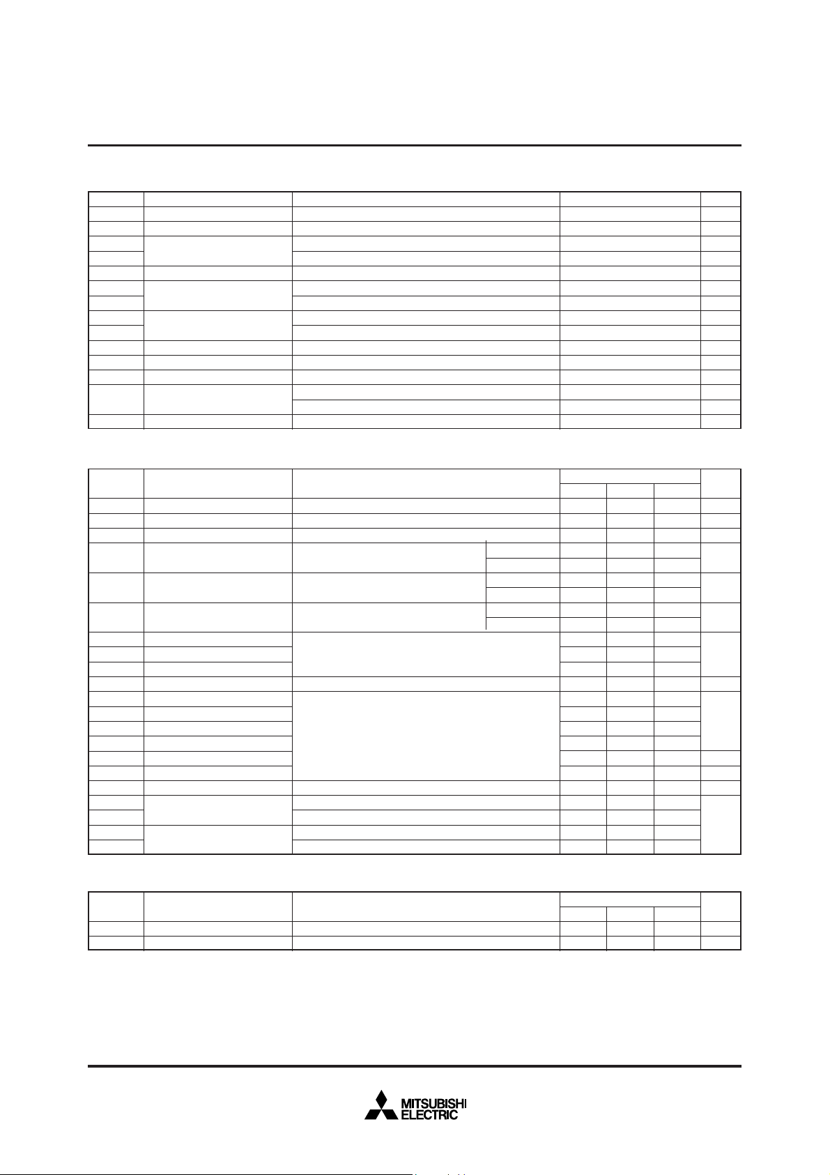
OUTLINE DRAWING & CIRCUIT DIAGRAM
110
±0.25
97
70.9
36
10
30
NP
13
14
5-6.5
38
9.2
UV
1414
32 3216.5
14
202020
B
3
(8.7)
(6)
3.96
W
4
MOUNTINGHOLES
CIRCUIT DIAGRAM
P
(17.5)
4-φ6.5
(14.5)
7-M6NUTS
6.5
(6)(6)
22.75
15.2
16.5
16 1632
36
10
30
7 7
(15.8)
6.5
3
7
1216
A
25
6.5
11.5
4
(14.5)
22.57
9.1
±0.25
90
80
75
67
Tc measured point
Housing Type of A and B
(Tyco Electronics P/N:)
A: 917353-1
B: 179838-1
Dimensions in mm
±1.0
35
+1.0
26
−0.5
LABEL
14
(SCREWING DEPTH)
(7)G
(1)S
(10)G
(4)S
U
P
U
P
U
N
U
N
N
(8)G
V
P
(2)SVP
UVW
V
(11)G
V
N
(5)S
(9)G
W
P
(3)S
W
P
N
(12)G
(6)S
W
N
W
N
(13)
(14)
(1)SUP
U
(7)G
(13)TH1
P
(2)S
V
P
V
P
(8)G
(14)TH2
(3)S
(9)G
(4)S
W
P
W
P
(10)G
(5)S
U
N
U
N
(11)G
V
N
V
N
(6)S
W
N
(12)GWN
A
B
Mar. 2013
ABSOLUTE MAXIMUM RATINGS (Tj = 25°C unless otherwise specified.)
Symbol
V
DSS
VGSS
ID
IDM
IDA
1
IS*
ISM*
4
PD*
4
PD*
Tch
Tstg
Visol
—
—
Drain-source voltage
Gate-source voltage
Drain current
Avalanche current
Source current
1
Maximum power dissipation
Channel temperature
Storage temperature
Isolation voltage
Mounting torque
Weight
G-S Short
D-S Short
T
C’ = 122°C*
Pulse*
3
2
L = 10µH Pulse*
2
Pulse*
TC = 25°C
T
C’ = 25°C*
3
Main terminal to base plate, AC 1 min, f=60Hz, RMS
Main Terminal M6
Mounting to heat sink M6
Typical value
ConditionsItem
2
ELECTRICAL CHARACTERISTICS (Tj = 25°C unless otherwise specified.)
ConditionsItemSymbol
DSS
I
VGS(th)
IGSS
rDS(on)
(chip)
VDS(on)
(chip)
RDD'-SS'
Ciss
Coss
Crss
QG
td(on)
tr
td(off)
tf
1
trr*
1
Qrr*
1
VSD*
Rth(j-c)
Rth(j-c’)
Rth(c-s)
Rth(c’-s’)
Drain cutoff current
Gate-source threshold voltage
Gate leakage current
Static drain-source
On-state resistance
Static drain-source
On-state voltage
Internal lead resistance
Input capacitance
Output capacitance
Reverse transfer capacitance
Total gate charge
Turn-on delay time
Rise time
Turn-off delay time
Fall time
Reverse recovery time
Reverse recovery charge
Source-drain voltage
Thermal resistance
Contact thermal resistance
V
DS = VDSS, VGS = 0V
I
D = 10mA, VDS = 10V
V
GS = VGSS, VDS = 0V
I
D = 100A
V
GS = 15V
I
D = 100A
V
GS = 15V
I
D = 100A
terminal-chip
V
DS = 10V
V
GS = 0V
V
DD = 80V, ID = 100A, VGS = 15V
DD = 80V, ID = 100A, VGS1 = VGS2 = 15V
V
R
G = 13Ω, Inductive load switching operation
I
S = 100A
S = 100A, VGS = 0V
I
MOSFET part (1/6 module)*
MOSFET part (1/6 module)*
7
3
Case to fin, Thermal grease Applied*8 (1/6 module)
Case to fin, Thermal grease Applied*
Tj = 25°C
Tj = 125°C
Tj = 25°C
Tj = 125°C
Tj = 25°C
Tj = 125°C
3, *8
(1/6 module)
MITSUBISHI <MOSFET MODULE>
FM200TU-3A
HIGH POWER SWITCHING USE
INSULATED PACKAGE
Min.
—
4.7
—
—
—
—
—
—
—
—
—
—
—
—
—
—
—
—
—
—
—
—
—
—
Rating
150
±20
100
200
100
100
200
410
560
–40 ~ +150
–40 ~ +125
2500
3.5 ~ 4.5
3.5 ~ 4.5
600
Limits
Typ.
—
6
—
4.8
9.1
0.48
0.91
1.2
1.68
—
—
—
820
—
—
—
—
—
6.5
—
—
—
0.1
0.09
Max.
0.66
400
250
450
200
200
0.30
0.22
7.3
1.5
6.6
—
—
—
—
50
—
—
1.3
—
—
Unit
V
V
A
A
A
A
A
W
W
°C
°C
V
N • m
N • m
g
Unit
1
mA
V
µA
mΩ
V
mΩ
7
nF
4
nC
ns
ns
µC
V
K/W
NTC THERMISTOR PART
Symbol
6
R25*
6
B*
1: It is characteristics of the anti-parallel, source to drain free-wheel diode (FWDi).
*
2: Pulse width and repetition rate should be such that the device junction temperature (Tj) does not exceed Tj max rating.
*
3: TC’ measured point is just under the chips. If use this value, Rth(s-a) should be measured just under the chips.
*
4: Pulse width and repetition rate should be such as to cause negligible temperature rise.
*
5: TTH is thermistor temperature.
*
6: B = (InR1-InR2)/(1/T1-1/T2) R1: Resistance at T1(K), R2: Resistance at T2(K)
*
7: TC measured point is shown in page OUTLINE DRAWING.
*
8: Typical value is measured by using thermally conductive grease of λ=0.9 W/(m·K).
*
Resistance
B Constant
TTH = 25°C*
Resistance at TTH = 25°C, 50°C*
5
ConditionsParameter
5
Min.
—
—
Limits
Typ.
100
4000
Max.
—
—
Unit
kΩ
K
Mar. 2013
 Loading...