

Mitsubishi Electric US, Inc CM400DY-24NF Data Sheet
CM400DY-24NF
MITSUBISHI IGBT MODULES
CM400DY-24NF
HIGH POWER SWITCHING USE
¡IC ...................................................................400A
CES ......................................................... 1200V
¡V
¡Insulated Type
¡2-elements in a pack
APPLICATION
General purpose inverters & Servo controls, etc
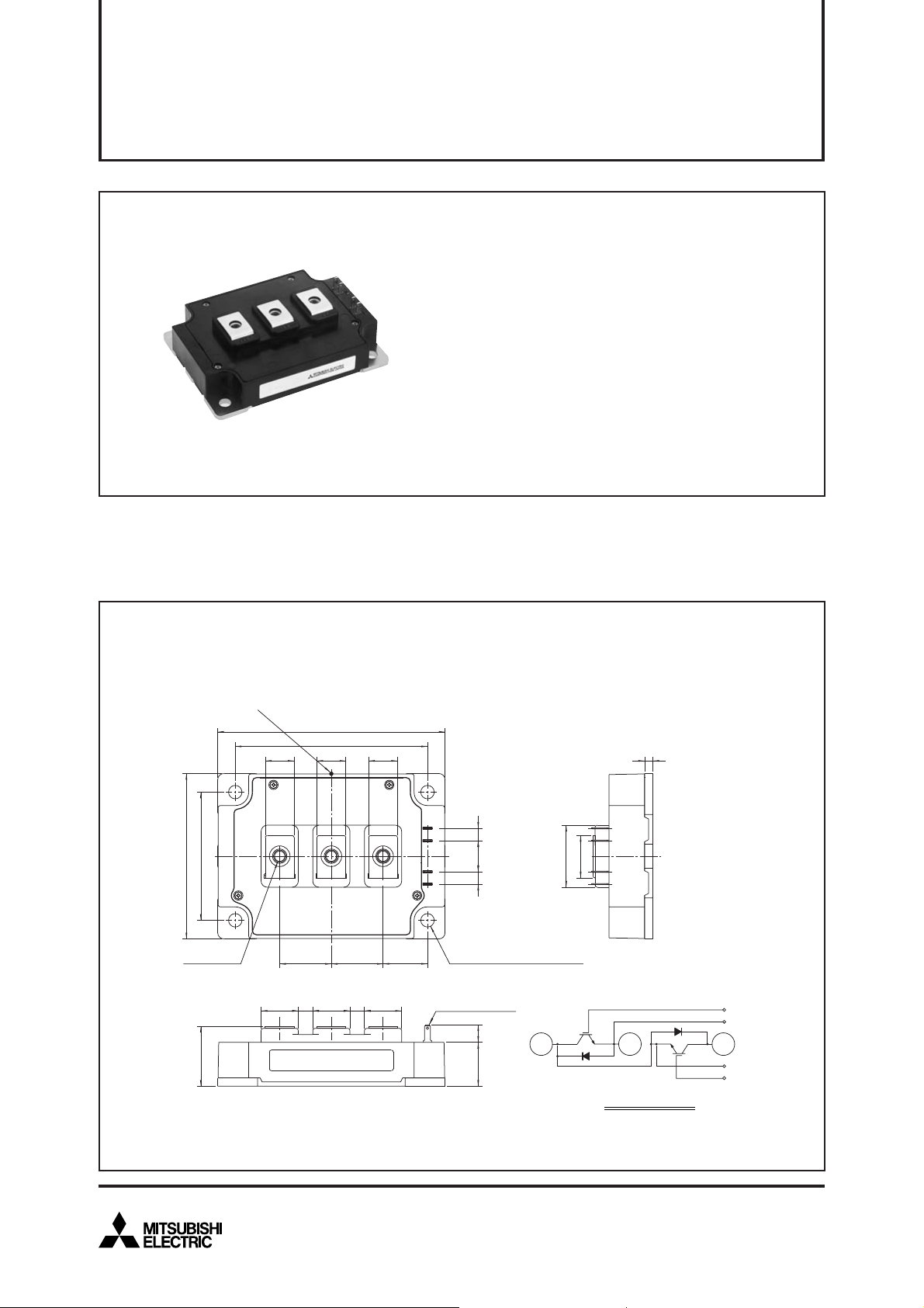
OUTLINE DRAWING & CIRCUIT DIAGRAM
Tc measured point (Base plate)
110
93
±0.25
80
62
3-M6 NUTS
±0.25
25 25
141414
G2G1 E2E1
C1E2C2E1
21.5
4-φ6.5 MOUNTING HOLES
Dimensions in mm
4
30
6 15 6
(20.5)
+1.0
29
–0.5
LABEL
18718718
TAB #110. t=0.5
8.521.2
1
C2E1
E2
CIRCUIT DIAGRAM
E2 G2G1 E1
C1
Feb. 2009
MITSUBISHI IGBT MODULES
CM400DY-24NF
HIGH POWER SWITCHING USE
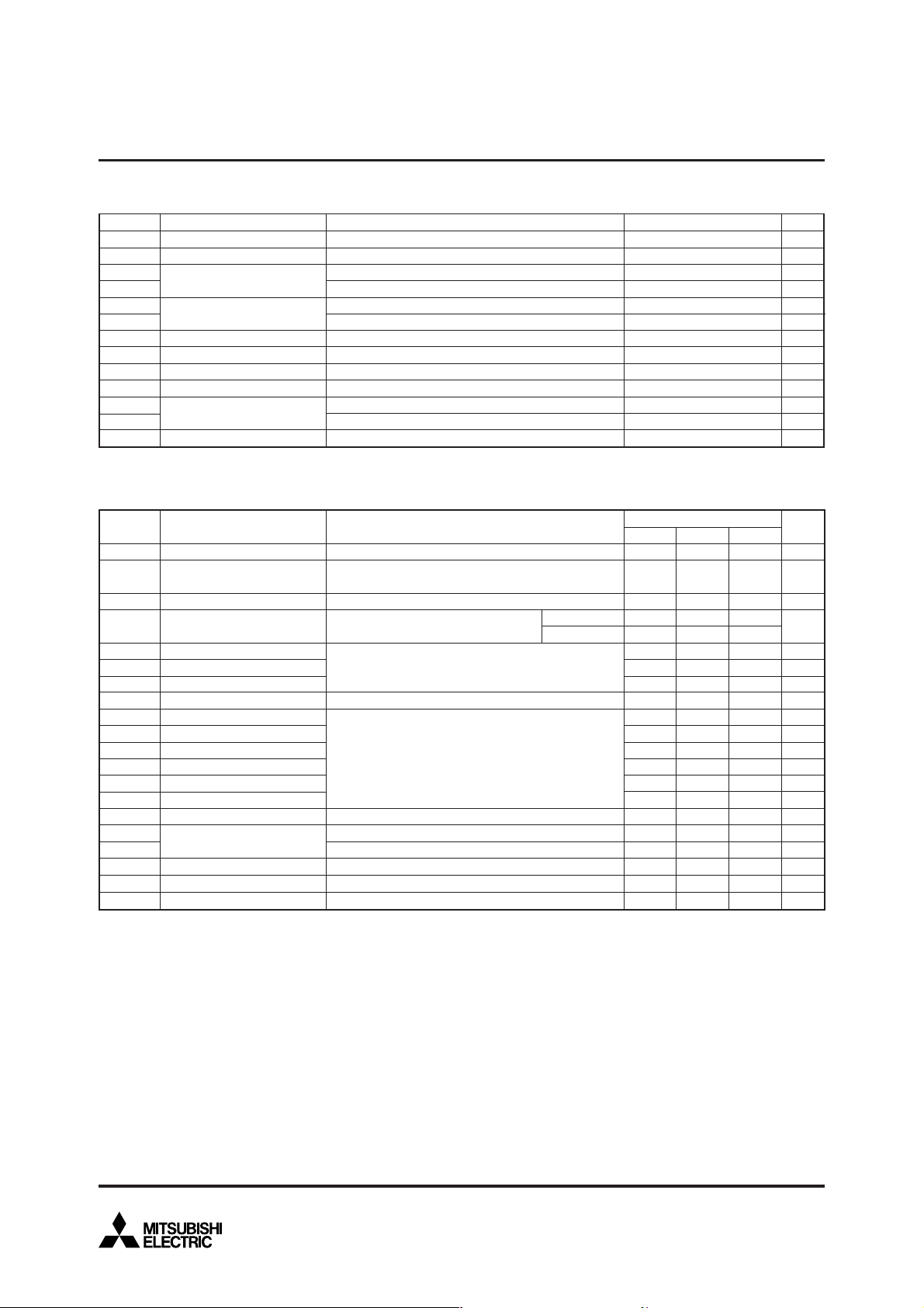
MAXIMUM RATINGS
Symbol Parameter
CES
V
VGES
IC
ICM
IE (
IEM (
PC (
Tj
Tstg
Viso
Collector-emitter voltage
Gate-emitter voltage
Collector current
Note 1
)
Emitter current
Note 1
)
Maximum collector dissipation
Note 3
)
Junction temperature
Storage temperature
Isolation voltage
—
Torque strength
—
—
Weight
ELECTRICAL CHARACTERISTICS
Symbol
I
CES
V
GE(th)
IGES
VCE(sat)
Cies
Coes
Cres
QG
td(on)
tr
td(off)
tf
trr (
Qrr (
VEC(
Rth(j-c)Q
R
th(j-c)R
R
th(c-f)
Rth(j-c’)Q
G
R
1 : Case temperature (Tc) measured point is shown in page OUTLINE DRAWING.
*
2 : Typical value is measured by using thermally conductive grease of λ = 0.9[W/(m • K)].
*
3 : Case temperature (Tc’) measured point is just under the chips.
*
If you use this value, R
Note 1. I
Collector cutoff current
Gate-emitter threshold voltage
Gate leakage current
Collector-emitter saturation voltage
Input capacitance
Output capacitance
Reverse transfer capacitance
Total gate charge
Turn-on delay time
Turn-on rise time
Turn-off delay time
Turn-off fall time
Note 1
)
Reverse recovery time
Note 1
)
Reverse recovery charge
Note 1
)
Emitter-collector voltage
Thermal resistance
Contact thermal resistance
Thermal resistance
External gate resistance
E, IEM, VEC, trr & Qrr represent characteristics of the anti-parallel, emitter-collector free-wheel diode (FWDi).
2. Pulse width and repetition rate should be such that the device junction temperature (T
3. Junction temperature (T
(Tj = 25°C, unless otherwise specified)
G-E Short
C-E Short
DC, T
C’ = 111°C
Pulse (Note 2)
Pulse (Note 2)
C = 25°C
T
Terminals to base plate, f = 60Hz, AC 1 minute
Main terminals M6 screw
Mounting M6 screw
Typical value
(Tj = 25°C, unless otherwise specified)
Parameter
VCE = VCES, VGE = 0V
C = 40mA, VCE = 10V
I
GE = VGES, VCE = 0V
±V
C = 400A, VGE = 15V
I
CE = 10V
V
V
GE = 0V
CC = 600V, IC = 400A, VGE = 15V
V
CC = 600V, IC = 400A
V
V
GE = ±15V
R
G = 0.78Ω, Inductive load
I
E = 400A
I
E = 400A, VGE = 0V
*1
IGBT part (1/2 module)
FWDi part (1/2 module)
Case to heat sink, Thermal compound Applied*2 (1/2 module)
Case temperature measured point is just under the chips
th(f-a) should be measured just under the chips.
j) should not increase beyond 150°C.
Conditions UnitRatings
*3
Test conditions
–40 ~ +150
–40 ~ +125
Min. Max.
—
68
—
T
j = 25°C
T
j = 125°C
—
—
—
—
—
—
—
—
—
—
—
—
—
—
—
—
—
0.78
j) does not exceed Tjmax rating.
1200
±20
400
800
400
800
1470
V
V
A
A
A
A
W
°C
°C
2500
3.5 ~ 4.5
3.5 ~ 4.5
580
Limits
Typ.
—
Vrms
N • m
N • m
g
Unit
1
mA
7V
—
1.8
2.0
—
—
—
2700
—
—
—
—
—
16
—
—
—
0.02
—
—
0.5
2.5
—
94
8
1.8
—
600
160
700
350
250
—
3.2
0.085
0.15
—
0.034
7.8
µA
V
nF
nF
nF
nC
ns
ns
ns
ns
ns
µC
V
K/W
K/W
K/W
*3
K/W
Ω
Feb. 2009
2
 Loading...