

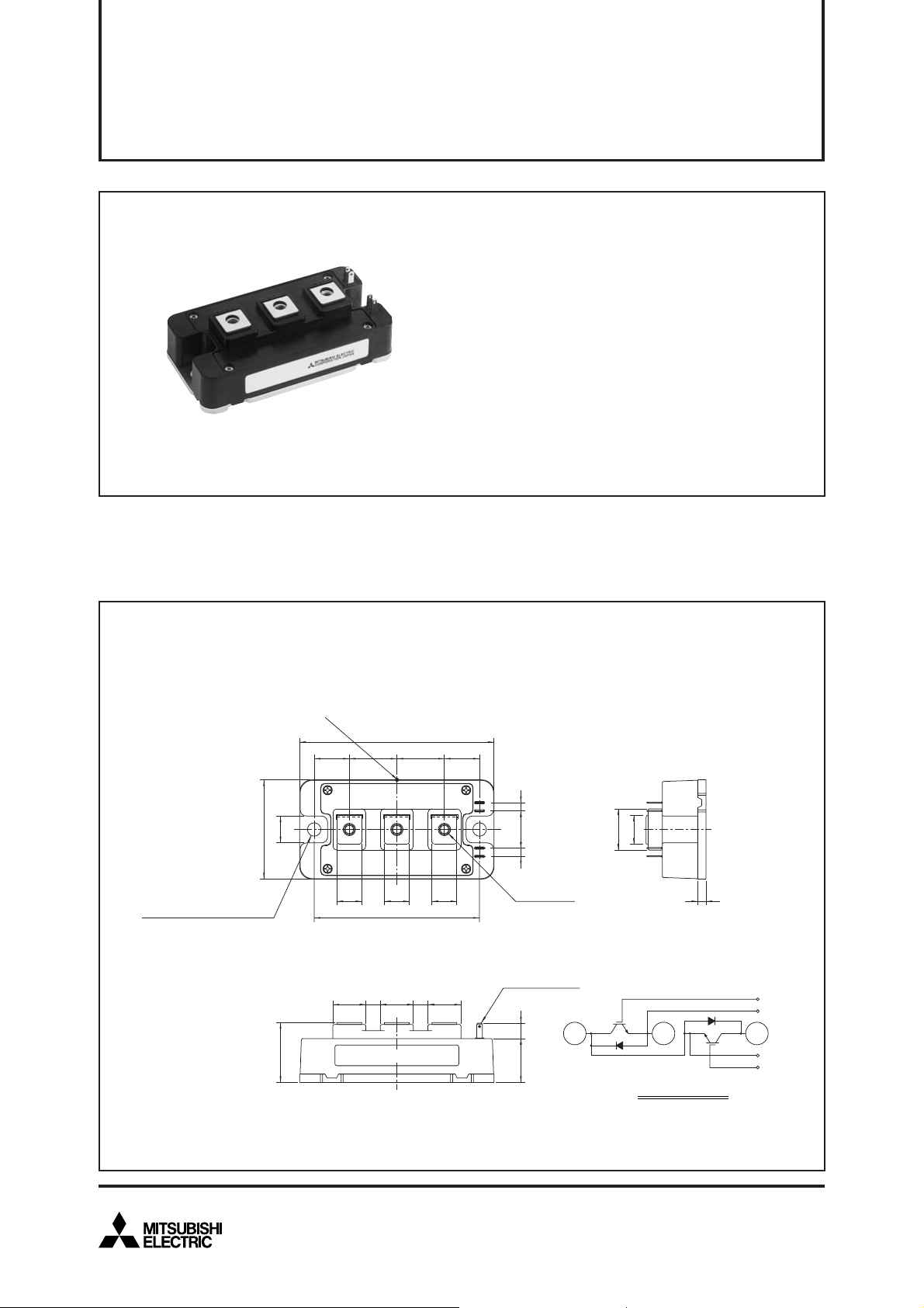
CM300DY-12NF
MITSUBISHI IGBT MODULES
CM300DY-12NF
HIGH POWER SWITCHING USE
¡IC ...................................................................300A
CES ............................................................ 600V
¡V
¡Insulated Type
¡2-elements in a pack
APPLICATION
General purpose inverters & Servo controls, etc
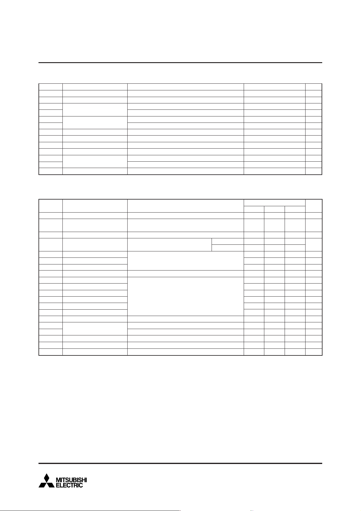
OUTLINE DRAWING & CIRCUIT DIAGRAM
Tc measured point (Base plate)
94
17
232317
C1
0.25
2-φ6.5 MOUNTING HOLES
C2E1
13
48
12 12 12
E2
80±
E2 G2
E1G1
4184
3-M5 NUTS
Dimensions in mm
20
(14)
4
+1.0
29
–0.5
16 7 16 7 16
LABEL
TAB #110. t=0.5
E2 G2G1 E1
C2E1
21.2 7.5
E2
CIRCUIT DIAGRAM
C1
Feb. 2009
1
MITSUBISHI IGBT MODULES
CM300DY-12NF
HIGH POWER SWITCHING USE
MAXIMUM RATINGS
Symbol Parameter
CES
V
VGES
IC
ICM
IE (
IEM (
PC (
Tj
Tstg
Viso
Collector-emitter voltage
Gate-emitter voltage
Collector current
Note 1
)
Emitter current
Note 1
)
Maximum collector dissipation
Note 3
)
Junction temperature
Storage temperature
Isolation voltage
—
Torque strength
—
—
Weight
ELECTRICAL CHARACTERISTICS
Symbol
ICES
V
GE(th)
IGES
VCE(sat)
Cies
Coes
Cres
QG
td(on)
tr
td(off)
tf
trr (
Qrr (
VEC(
Rth(j-c)Q
R
th(j-c)R
R
th(c-f)
Rth(j-c’)Q
R
G
1 : Case temperature (Tc) measured point is shown in page OUTLINE DRAWING.
*
2 : Typical value is measured by using thermally conductive grease of λ = 0.9[W/(m • K)].
*
3 : Case temperature (Tc’) measured point is just under the chips.
*
Note 1. I
Collector cutoff current
Gate-emitter threshold voltage
Gate leakage current
Collector-emitter saturation voltage
Input capacitance
Output capacitance
Reverse transfer capacitance
Total gate charge
Turn-on delay time
Turn-on rise time
Turn-off delay time
Turn-off fall time
Reverse recovery time
Note 1
)
Reverse recovery charge
Note 1
)
Emitter-collector voltage
Note 1
)
Thermal resistance
Contact thermal resistance
Thermal resistance
External gate resistance
If you use this value, R
E, VEC, trr & Qrr represent characteristics of the anti-parallel, emitter-collector free-wheel diode (FWDi).
2. Pulse width and repetition rate should be such that the device junction temperature (T
3. Junction temperature (T
(Tj = 25°C, unless otherwise specified)
G-E Short
C-E Short
DC, T
C’ = 89°C
Pulse (Note 2)
Pulse (Note 2)
C = 25°C
T
Terminals to base plate, f = 60Hz, AC 1 minute
Main terminals M5 screw
Mounting M6 screw
Typical value
(Tj = 25°C, unless otherwise specified)
Parameter
CE = VCES, VGE = 0V
V
C = 30mA, VCE = 10V
I
GE = VGES, VCE = 0V
±V
C = 300A, VGE = 15V
I
CE = 10V
V
V
GE = 0V
CC = 300V, IC = 300A, VGE = 15V
V
CC = 300V, IC = 300A
V
V
GE = ±15V
R
G = 2.1Ω, Inductive load
I
E = 300A
I
E = 300A, VGE = 0V
*1
IGBT part (1/2 module)
FWDi part (1/2 module)
Case to heat sink, Thermal compound Applied*2 (1/2 module)
Case temperature measured point is just under the chips
th(f-a) should be measured just under the chips.
j) should not increase beyond 150°C.
Conditions UnitRatings
*3
Test conditions
–40 ~ +150
–40 ~ +125
Min. Max.
—
5 7.5
—
T
j = 25°C
T
j = 125°C
—
—
—
—
—
—
—
—
—
—
—
—
—
—
—
—
—
2.1
j) does not exceed Tjmax rating.
600
±20
300
600
300
600
780
V
V
A
A
A
A
W
°C
°C
2500
2.5 ~ 3.5
3.5 ~ 4.5
310
Limits
Typ.
—
Vrms
N • m
N • m
g
Unit
1
mA
6V
—
1.7
1.7
—
—
—
1200
—
—
—
—
—
5.5
—
—
—
0.07
—
—
0.5
2.2
—
45
5.5
1.8
—
120
120
350
300
150
—
2.6
0.16
0.25
—
0.093
21
µA
V
nF
nF
nF
nC
ns
ns
ns
ns
ns
µC
V
K/W
K/W
K/W
*3
K/W
Ω
Feb. 2009
2

PERFORMANCE CURVES
OUTPUT CHARACTERISTICS
600
VGE =
20V
500
400
(TYPICAL)
15
13
Tj = 25°C
12
MITSUBISHI IGBT MODULES
CM300DY-12NF
HIGH POWER SWITCHING USE
COLLECTOR-EMITTER SATURATION
(V)
CE (sat)
VOLTAGE CHARACTERISTICS
4
VGE = 15V
3
(TYPICAL)
300
200
100
COLLECTOR CURRENT IC (A)
0
046810
2
COLLECTOR-EMITTER VOLTAGE V
COLLECTOR-EMITTER SATURATION
VOLTAGE CHARACTERISTICS
(TYPICAL)
10
(V)
8
CE (sat)
6
4
COLLECTOR-EMITTER
2
SATURATION VOLTAGE V
0
Tj = 25°C
IC = 300A
IC = 600A
IC = 120A
11
10
8
9
CE
(V)
2
1
COLLECTOR-EMITTER
SATURATION VOLTAGE V
0
100
0 200 600400 500300
COLLECTOR CURRENT IC (A)
Tj = 25°C
T
j = 125°C
FREE-WHEEL DIODE
FORWARD CHARACTERISTICS
(TYPICAL)
3
10
7
5
3
2
2
10
7
5
3
EMITTER CURRENT IE (A)
2
1
2012 146810 16 18
10
012 435
Tj = 25°C
T
j = 125°C
GATE-EMITTER VOLTAGE V
CAPACITANCE–VCE
CHARACTERISTICS
2
10
7
5
(nF)
3
res
2
, C
1
10
oes
7
, C
5
ies
3
2
0
10
7
5
3
2
CAPACITANCE C
VGE = 0V
–1
10
–1
2
10
(TYPICAL)
0
10
357 2
357 2
COLLECTOR-EMITTER VOLTAGE V
10
1
GE
Cies
Coes
Cres
357
(V)
CE
10
(V)
EMITTER-COLLECTOR VOLTAGE V
EC
(V)
HALF-BRIDGE
SWITCHING CHARACTERISTICS
3
10
7
5
3
2
2
10
7
5
3
2
1
10
7
5
SWITCHING TIME (ns)
3
2
0
2
10
10
1
(TYPICAL)
2
10
57
tf
td(off)
td(on)
tr
Conditions:
V
CC = 300V
V
GE = ±15V
R
G = 2.1Ω
T
j = 125°C
Inductive load
23 5723
10
3
COLLECTOR CURRENT IC (A)
Feb. 2009
3

REVERSE RECOVERY CHARACTERISTICS
OF FREE-WHEEL DIODE
3
10
(A)
rr
7
(ns)
rr
5
3
2
2
10
7
5
3
2
REVERSE RECOVERY TIME t
1
10
REVERSE RECOVERY CURRENT l
1
10
(TYPICAL)
I
rr
t
rr
23 57
10
2
Conditions:
V
V
R
T
Inductive load
23 57
EMITTER CURRENT I
CC
= 300V
GE
= ±15V
G
= 2.1Ω
j
= 25°C
E
(A)
10
MITSUBISHI IGBT MODULES
CM300DY-12NF
HIGH POWER SWITCHING USE
TRANSIENT THERMAL
IMPEDANCE CHARACTERISTICS
(IGBT part & FWDi part)
10
10
10
10
10
1
–1
7
5
3
2
–2
7
5
3
2
–3
–3
–3
10
0
10
7
5
3
th (j–c)
2
–1
10
7
5
3
2
IGBT part:
–2
10
Per unit base =
7
R
5
NORMALIZED TRANSIENT
3
FWDi part:
3
Per unit base =
THERMAL IMPEDANCE Z
2
R
–3
10
–2
23 57 23 57 23 57 23 57
10
th(j– c)
= 0.16K/W
th(j– c)
= 0.25K/W
10
10
–1
–5
0
10
Single Pulse
T
C
= 25°C
–4
23 57 23 57
10
TIME (s)
GATE CHARGE
CHARACTERISTICS
(TYPICAL)
20
IC = 300A
(V)
GE
16
VCC = 200V
12
8
4
GATE-EMITTER VOLTAGE V
0
0
400
200
600
800
GATE CHARGE QG (nC)
VCC = 300V
1200 1600
14001000
Feb. 2009
4
 Loading...