


<IGBT Modules>
Publication Date : September 2017
CMH-11232-A
Ver.1.1
1 0
0
1 0
0
APPLICATION
OPTION (Below options are available.)
INTERNAL CONNECTION
Terminal code
12
3
11
NTC
7
8
10
9
16
2
15
14
13
20
1
19
18
17
21
22 4
6
5
1 U 13
EVN 2 V 14
GVN 3 W
15
EVP 4 B
16
GVP 5 EB
17
EUN 6 GB
18
GUN 7 TH1
19
EUP 8 TH2
20
GUP 9 EWN
21 P 10
GWN
22 N 11
EWP
23
EVN
12
GWP
CM100RX-24T/CM100RXP-24T
HIGH POWER SWITCHING USE
INSULATED TYPE
Collector current IC .............…..................…
Collector-emitter voltage V
Maximum junction temperature T
RX
●Flat base type
●Copper base plate (Nickel-plating)
●RoHS Directive compliant
●Tin-plating pin terminals
..................
CES
vjmax
.........
1 2 0 0
1 7 5
A
V
°C
RXP
sevenpack (three-phase bridge+Brake chopper)
AC Motor Control, Motion/Servo Control, Power supply, etc.
●PC-TIM (Phase Change Thermal Interface Material) pre-apply
Collector current IC .............…..................…
Collector-emitter voltage V
Maximum junction temperature T
..................
CES
vjmax
.........
1 2 0 0
1 7 5
A
V
°C
●Flat base type
●Copper base plate (Nickel-plating)
●RoHS Directive compliant
●Tin-plating pressfit terminals
●UL Recognized under UL1557, File No. E323585
1
<IGBT Modules>
CM100RX-24T/CM100RXP-24T
HIGH POWER SWITCHING USE
INSULATED TYPE
Publication Date : September 2017
CMH-11232-A
Ver.1.1
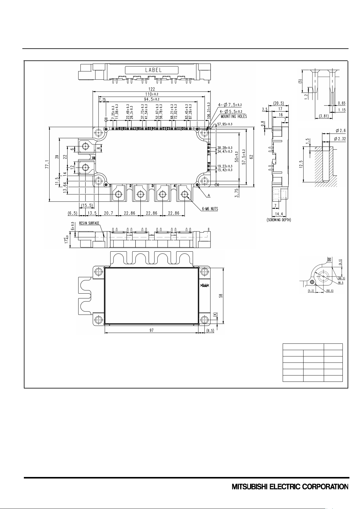
OUTLINE DRAWING
Dimension in mm
TERMINAL
SECTION A
MOUNTING HOLES
over 3
to 6
±0.3
over 30
to 120
±0.8
RX
Tolerance otherwise specified
Division of Dimension Tolerance
0.5 to 3 ±0.2
over 6 to 30 ±0.5
over 120 to 400 ±1.2
2
<IGBT Modules>
CM100RX-24T/CM100RXP-24T
HIGH POWER SWITCHING USE
INSULATED TYPE
Publication Date : September 2017
CMH-11232-A
Ver.1.1
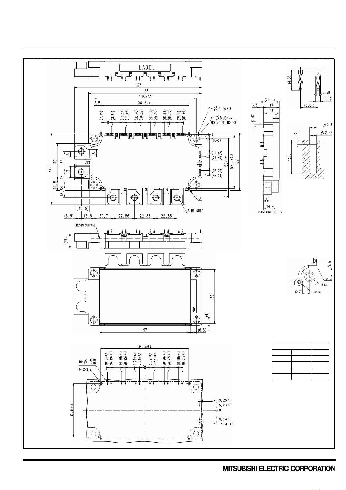
OUTLINE DRAWING
Dimension in mm
TERMINAL
SECTION A
MOUNTING HOLES
0.5
to 3
±0.2
RXP
PCB DRILL HOLE PATTERN Tolerance otherwise specified
Division of Dimension Tolerance
over 3 to 6 ±0.3
over 6 to 30 ±0.5
over 30 to 120 ±0.8
over 120 to 400 ±1.2
3
<IGBT Modules>
CM100RX-24T/CM100RXP-24T
HIGH POWER SWITCHING USE
INSULATED TYPE
Publication Date : September 2017
CMH-11232-A
Ver.1.1
Symbol
Item
Conditions
Rating
Unit V
Collector-emitter voltage
G-E short-circuited
1200
V
V
Gate-emitter voltage
C-E short-circuited
± 20
V IC
DC, TC=119 °C
100
I
CRM
Pulse, Repetitive
200
P
Total power dissipation
TC=25 °C
565
W
IE
DC
100
I
Pulse, Repetitive
200
Symbol
Item
Conditions
Rating
Unit
V
CES
Collector-emitter voltage
G-E short-circuited
1200
V V
Gate-emitter voltage
C-E short-circuited
± 20
V IC
DC, TC=121 °C
75
I
CRM
Pulse, Repetitive
150
P
tot
Total power dissipation
TC=25 °C
440
W V
Repetitive peak reverse voltage
G-E short-circuited
1200
V IF
DC
75
I
Pulse, Repetitive
150
Symbol
Item
Conditions
Rating
Unit V
Isolation voltage
Terminals to base plate, RMS, f=60 Hz, AC 1 min
2500
V
T
Maximum junction temperature
Instantaneous event (overload)
175
T
Maximum case temperature
(Note4)
125
T
vjop
Operating junction temperature
Continuous operation (under switching)
-40 ~ +150
T
Storage temperature
-
-40 ~ +125
Limits
Min.
Typ.
Max.
I
Collector-emitter cut-off current
VCE=V
, G-E short-circuited
- - 1.0
mA I
GES
Gate-emitter leakage current
VGE=V
, C-E short-circuited
- - 0.5
μA
V
GE(th)
Gate-emitter threshold voltage
IC=10 mA, VCE=10 V
5.4
6.0
6.6
V
IC=100 A, VGE=15 V,
Tvj=25 °C
-
1.60
1.95
Refer to the figure of test circuit
Tvj=125 °C
-
1.80 - V
(Note5)
Tvj=150 °C
-
1.85 -
IC=100 A,
Tvj=25 °C
-
1.55
1.80
VGE=15 V,
Tvj=125 °C
-
1.75 - V
Tvj=150 °C
-
1.80 -
C
oes
Output capacitance
VCE=10 V, G-E short-circuited
- - 0.8
nF C
Reverse transfer capacitance
- -
0.3
QG
Gate charge
VCC=600 V, IC=100 A, VGE=15 V
-
0.75 - μC t
d(on)
Turn-on delay time
- - 400
tr
Rise time
- - 200
t
Turn-off delay time
- - 500
tf
Fall time
- - 500
MAXIMUM RATINGS (Tvj=25 °C, unless otherwise specified)
INVERTER PART IGBT/FWD
CES
GES
Collector current
tot
(Note1)
ERM
(Note1)
Emitter current
BRAKE PART IGBT/DIODE
(Note2, 4)
(Note2)
(Note2, 4)
(Note3)
(Note3)
A
A
FRM
GES
Collector current
RRM
(Note2)
Forward current
(Note2, 4)
(Note3)
(Note2, 4)
(Note3)
MODULE
isol
vjmax
Cmax
stg
ELECTRICAL CHARACTERISTICS (Tvj=25 °C, unless otherwise specified)
INVERTER PART IGBT/FWD
Symbol Item Conditions
CES
V
CEsat
(Terminal)
Collector-emitter saturation voltage
V
CEsat
(Chip)
C
Input capacitance - - 22.8
ies
CES
GES
(Note5)
A
A
°C
°C
Unit
res
d(off)
VCC=600 V, IC=100 A, VGE=±15 V,
RG=3.9 Ω, Inductive load
4
ns
<IGBT Modules>
CM100RX-24T/CM100RXP-24T
HIGH POWER SWITCHING USE
INSULATED TYPE
Publication Date : September 2017
CMH-11232-A
Ver.1.1
Limits
Min.
Typ.
Max.
IE=100 A, G-E short-circuited,
Tvj=25 °C
-
1.50
1.95
Refer to the figure of test circuit
Tvj=125 °C
-
1.60 - V
Tvj=150 °C
-
1.65 -
IE=100 A,
Tvj=25 °C
-
1.45
1.75
G-E short-circuited,
Tvj=125 °C
-
1.45 - V
Tvj=150 °C
-
1.45 -
t
rr
Reverse recovery time
VCC=600 V, IE=100 A, VGE=±15 V,
- - 300
ns Qrr
(Note1)
Reverse recovery charge
RG=3.9 Ω, Inductive load
-
12 - μC
Eon
Turn-on s witching energy per pulse
VCC=600 V, IC=IE=100 A,
-
9.2
-
E
Turn-off switching energy per pulse
VGE=±15 V, RG=3.9 Ω, Tvj=150 °C,
-
10.4
-
Err
Reverse recovery energy per pulse
Inductive load
-
8.2 - mJ R
Internal lead resistance
Main terminals-chip, per switch, TC=25 °C
-
2.0 - mΩ
rg
Internal gate resistance
Per switch
- 0 - Ω
Limits
Min.
Typ.
Max.
I
CES
Collector-emitter cut-off current
VCE=V
, G-E short-circuited
- - 1.0
mA I
Gate-emitter leakage current
VGE=V
, C-E short-circuited
- - 0.5
μA V
Gate-emitter threshold voltage
IC=7.5 mA, VCE=10 V
5.4
6.0
6.6
V
IC=75 A, VGE=15 V,
Tvj=25 °C
-
1.65
2.00
Refer to the figure of test circuit
Tvj=125 °C
-
1.80 - V
Tvj=150 °C
-
1.85 -
IC=75 A,
Tvj=25 °C
-
1.60
1.85
VGE=15 V,
Tvj=125 °C
-
1.75 - V
Tvj=150 °C
-
1.80 - C
Input capacitance
- -
18.2
C
Output capacitance
VCE=10 V, G-E short-circuited
- - 0.5
nF
C
res
Reverse transfer capacitance
- -
0.2
QG
Gate charge
VCC=600 V, IC=75 A, VGE=15 V
-
0.57 - μC t
Turn-on delay time
- - 400
tr
Rise time
- - 200
t
d(off)
Turn-off delay time
- - 500
tf
Fall time
- - 500
Eon
Turn-on s witching energy per pulse
VCC=600 V, IC=75 A, VGE=±15 V,
-
9.3
-
E
Turn-off switching energy per pulse
RG=5.6 Ω, Tvj=150 °C, Inductive load
-
7.8
-
rg
Internal gate resistance
- - 4.0 - Ω
I
RRM
Reverse current
VR=V
RRM
, G-E short-circuited
- - 1.0
mA
IF=75 A, G-E short-circuited,
Tvj=25 °C
-
1.65
2.10
Refer to the figure of test circuit
Tvj=125 °C
-
1.80 - V
Tvj=150 °C
-
1.85 -
IF=75 A,
Tvj=25 °C
-
1.50
1.90
G-E short-circuited,
Tvj=125 °C
-
1.50 - V
Tvj=150 °C
-
1.50 -
trr
Reverse recovery time
VCC=600 V, IF=75 A, VGE=±15 V,
- - 300
ns
Qrr
Reverse recovery charge
RG=5.6 Ω, Inductive load
-
8.0 - μC
VCC=600 V, IF=75 A, VGE=±15 V,
RG=5.6 Ω, Tvj=150 °C, Inductive load
ELECTRICAL CHARACTERISTICS (cont.; Tvj=25 °C, unless otherwise specified)
INVERTER PART IGBT/FWD
Symbol Item Conditions
(Note1)
VEC
(Terminal)
(Note5)
Emitter-collector voltage
(Note1)
VEC
(Chip)
(Note1)
off
(Note1)
CC'+EE'
(Note5)
BRAKE PART IGBT/DIODE
Symbol Item Conditions
CES
GES
GE(th)
V
CEsat
(Terminal)
V
CEsat
(Chip)
ies
oes
Collector-emitter saturation voltage
GES
(Note5)
(Note5)
Unit
mJ
(Note4)
Unit
d(on)
off
V
F
(Terminal)
Forward voltage
V
F
(Chip)
Err Reverse recovery energy per pulse
VCC=600 V, IC=75 A, VGE=±15 V,
RG=5.6 Ω, Inductive load
(Note5)
(Note5)
5
ns
mJ
- 5.2 - mJ
<IGBT Modules>
CM100RX-24T/CM100RXP-24T
HIGH POWER SWITCHING USE
INSULATED TYPE
Publication Date : September 2017
CMH-11232-A
Ver.1.1
Limits
Min.
Typ.
Max.
R25
Zero-power resistance
TC=25 °C
4.85
5.00
5.15
kΩ ΔR/R
Deviation of resistance
R
=493 Ω, TC=100 °C
-7.3 - +7.8
%
B
(25/50)
B-constant
Approximate by equation
-
3375 - K P25
Power dissipation
TC=25 °C
- - 10
mW
Limits
Min.
Typ.
Max.
R
th(j- c)Q
Junction to case, per Inverter IGBT
- - 264
R
th(j- c)D
Junction to case, per Inverter FWD
- - 391
R
Junction to case, Brake IGBT
- - 339
R
Junction to case, Brake DIODE
- - 480
Case to heat sink,
Thermal grease applied
-
11.5
-
per 1 module,
PC-TIM applied
(Note4, 8)
-
3.1
-
Limits
Min.
Typ.
Max.
Mt
Mounting torque
Main terminals
M 6 screw
3.5
4.0
4.5
N·m
Ms
Mounting torque
Mounting to heat sink
M 5 screw
2.5
3.0
3.5
N·m
Terminal to terminal
17 - -
Terminal to base plate
18.4 - -
Terminal to terminal
10 - -
Terminal to base plate
16.2 - -
ec
Flatness of base plate
On the centerline X, Y
±0 - +200
μm m
mass - -
330 - g
5.
Pulse width and repetition rate should be such as to cause negligible temperature rise. Refer to the figure of test circuit.
)
TT
/()
R
R
ln(B
)/(
502550
25
5025
11
−=
R50: resistance at absolute temperature T50 [K]; T50=50 [°C]+273.15=323.15 [K]
Y
X
+:Convex
-:Concave
+:Convex
-:Concave
Mounting side
Mounting side
Mounting side
2 mm
2 mm
ELECTRICAL CHARACTERISTICS (cont.; Tvj=25 °C, unless otherwise specified)
NTC THERMISTOR PART
Symbol Item Conditions
(Note4)
100
(Note4)
(Note4)
(Note6)
THERMAL RESISTANCE CHARACTERISTICS
Symbol Item Conditions
Thermal resistance
th(j- c)Q
th(j- c)D
R
th(c- s )
Thermal resistance
Contact thermal resistance
MECHANICAL CHARACTERISTICS
Symbol Item Conditions
ds Creepage distance
(Note4)
(Note4)
(Note4)
(Note4)
Unit
Unit
K/kW
K/kW
(Note4, 7)
K/kW
Unit
mm
da Clearance
(Note9)
*: This product is compliant with the Restriction of the Use of Certain Hazardous Substances in Electrical and Electronic Equipment (RoHS) directive 2011/65/EU.
Note1. Represent ratings and characteristics of the anti-parallel, emitter-collector free-wheeling diode (FWD).
2. Junction temperatu re (Tvj) should not increase beyond T
3. Pulse width and repetition rate should be such that the device junction temperature (Tvj) dose not exceed T
4. Case temperature (TC) and heat sink temperature (TS) are defined on the each surface (mounting side) of base plate and heat sink just under the chips.
Refer to the figure of chip location.
6.
R25: resistance at absolute temperature T25 [K]; T25=25 [°C]+273.15=298.15 [K]
7. Typical value is measured by usin g ther mally conductive grease of λ=0.9 W/(m·K)/D
8. Typical value is measured by usin g PC-TIM of λ=3.4 W/(m·K)/D
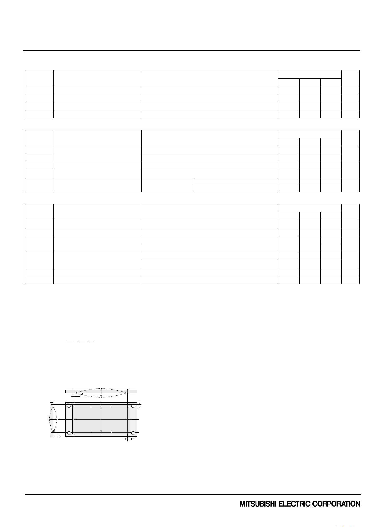
9. The base plate (mounting side) flatness measurement points (X, Y) are shown in the following figure.
rating.
vjmax
rating.
vjmax
=50 μm.
(C-S)
=50 μm.
(C-S)
mm
6

<IGBT Modules>
CM100RX-24T/CM100RXP-24T
HIGH POWER SWITCHING USE
INSULATED TYPE
Publication Date : September 2017
CMH-11232-A
Ver.1.1
Note10.
Use the following screws when mounting the printed circuit board (PCB) on the standoffs.
(1)
PT
K25×8
0.55 ± 0.055 N・m
(2)
PT
K25×10
0.75 ± 0.075 N・m
by handwork (equivalent to 30 rpm
DELTA PT
0.55 ± 0.055 N・m
DELTA PT
Limits
Min.
Typ.
Max.
VCC
(DC) Supply voltage
Applied across P-N terminals
-
600
850
V
Applied across
G*P-E*P/G*N-E*N/GB-EB terminals (*=U,V,W)
PCB thickness : t=1.6.
Type Size Tightening torque Recommended tightening method
(3)
(4)
(5) B1 tapping screw φ2.6×10 or φ2.6×12
RECOMMENDED OPERATING CONDITIONS
Symbol Item Conditions
V
Gate (-emitter drive) voltage
GEon
RG External gate resistance
25×8
25×10
by mechanical screw driver)
0.75 ± 0.075 N・m
0.75 ± 0.075 N・m
~ 600 rpm (by mechanical screw driver)
13.5 15.0 16.5 V
Inverter IGBT, Per switch 3.9 - 39
Brake IGBT 5.6 - 56
Unit
Ω
7

<IGBT Modules>
CM100RX-24T/CM100RXP-24T
HIGH POWER SWITCHING USE
INSULATED TYPE
Publication Date : September 2017
CMH-11232-A
Ver.1.1
CHIP LOCATION (Top view)
Dimension in mm, tolerance: ±1 mm
RX
RXP
Tr*P/Tr*N/TrBr: IGBT, Di*P/Di*N: FWD, DiBr: DIODE, Th: NTC thermistor
Option: PC-TIM applied baseplate outline
RX RXP
8

<IGBT Modules>
CM100RX-24T/CM100RXP-24T
HIGH POWER SWITCHING USE
INSULATED TYPE
Publication Date : September 2017
CMH-11232-A
Ver.1.1
VCC
-VGE
+VGE
-VGE
+
vCE
vGE
0
iE
iC
P
N
*
G*P
E*P
G*N
E*N
Load
RG
*: U, V , W
~
t
tf
tr
t
d(on)
iC
10%
90 %
90 %
vGE
~
~
~
0 V
0 A
0
t
d(off)
t
Irr
Qrr=0.5×Irr×trr
0.5×Irr
t
trr
iE
0 A
IE
0.1×ICM
ICM
VCC
vCE
iC
t
0
ti
0.1
×VCC
0.1×VCC
VCC
ICM
vCE
iC
t
0
0.02×ICM
ti
IEM
vEC
iE
t
0 V
ti
t
VCC
0 A
TEST CIRCUIT AND WAVEFORMS
Switching characteristics test circuit and waveforms trr, Qrr characteristics test waveform
IGBT T urn-on switching energy IGBT T urn-off switching energy FWD Reverse recovery energy
Switching energy and Reverse recovery energy test waveforms (Integral time instruction drawing)
9

<IGBT Modules>
CM100RX-24T/CM100RXP-24T
HIGH POWER SWITCHING USE
INSULATED TYPE
Publication Date : September 2017
CMH-11232-A
Ver.1.1
V
G-E short-
circuited
21
1
22
20
19
18
17
VGE=15 V
IC
V
G-E short-
circuited
21
2
22
16
15
14
13
VGE=15 V
IC
V
G-E short-
circuited
21
3
22
12
11
10
9
VGE=15 V
IC
TrUP TrVP TrWP
G-E short-
circuited
21
1
22
20
19
18
17
VGE=15 V
IC
V
G-E short-
circuited
21
2
22
16
15
14
13
VGE=15 V
IC
V
G-E short-
circuited
21
3
22
12
11
10
9
VGE=15 V
IC
V
21
4
22
6
5
VGE=15 V
IC
V
TrUN TrVN TrWN
Gate-emitter
GVP-EVP, GVN-EVN,
Gate-emitter
GUP-EUP, GUN-EUN,
Gate-emitter
GUP-EUP, GUN-EUN,
Gate-emitter
GUP-EUP, GUN-EUN,
short-circuited
GWP-EW P, GW N-EWN
short-circuited
GWP-EWP, GWN-EWN
short-circuited
GVP-EVP, GVN-EVN
short-circuited
GVP-EVP, GVN-EVN,
GB-EB
GB-EB
GB-EB
GWP-EW P, GW N-EWN
V
G-E short-
circuited
21
1
22
20
19
18
17
IE
G-E short-
circuited
V
G-E short-
circuited
21 2
22
16
15
14
13
IE
G-E short-
circuited
V
G-E short-
circuited
21
3
22
12
11
10
9
IE
G-E short-
circuited
DiUP DiVP DiWP
G-E short-
circuited
21
1
22
20
19
18
17
IE
V
G-E short-
circuited
G-E short-
circuited
21
2
22
16
15
14
13
IE
V
G-E short-
circuited
G-E short-
circuited
21
3
22
12
11
10
9
IE
V
G-E short-
circuited
21
4
22
6
5
IF
V
G-E short-
circuited
DiUN DiVN DiWN
Gate-emitter
GVP-EVP, GVN-EVN,
Gate-emitter
GUP-EUP, GUN-EUN,
Gate-emitter
GUP-EUP, GUN-EUN,
Gate-emitter
GUP-EUP, GUN-EUN,
short-circuited
GWP-EW P, GW N-EWN
short-circuited
GWP-EWP, GWN-EWN
short-circuited
GVP-EVP, GVN-EVN
short-circuited
GVP-EVP, GVN-EVN,
GB-EB
GB-EB
GB-EB
GWP-EW P, GW N-EWN
TEST CIRCUIT
V
CEsat
characteristics test circuit
VEC characteristics test circuit
VF characteristics test circuit
10

<IGBT Modules>
CM100RX-24T/CM100RXP-24T
HIGH POWER SWITCHING USE
INSULATED TYPE
Publication Date : September 2017
CMH-11232-A
Ver.1.1
OUTPUT CHARACTERISTICS
COLLECTOR-EM ITTER SATURATION VOLTAGE
(TYPICAL)
CHARACTERISTICS
(TYPICAL)
Tvj=25 °C
(chip)
VGE=15 V
(chip)
COLLECTOR CURRENT I
COLLECTOR
COLLECTOR-EMITTER VOLTAGE VCE (V)
COLLECTOR CURRENT IC (A)
COLLECTOR-EMITTER VO LTAGE CHARACTERISTICS
FREE WHEELING DIODE
(TYPICAL)
FORWARD CHARACTERISTICS
(TYPICAL)
Tvj=25 °C
(chip)
G-E short-circuited
(chip)
COLLECTOR
EMITTER CURRENT I
GATE-EMITTER VOLTAGE VGE (V)
EMITTER-COLL ECTOR VOL TAGE VEC (V)
Tvj=125 °C
Tvj=150 °C
Tvj=125 °C
IC=200 A
IC=100 A
IC=50 A
Tvj=150 °C
PERFORMANCE CURVES
INVERTER PART
(A)
C
VGE=20 V
15 V
12 V
13.5 V
11 V
10 V
9 V
8 V
(V)
CEsat
Tvj=25 °C
-EMITTER SATURATION VOLTAGE V
(V)
CE
-EMITTER VOLTAGE V
(A)
E
Tvj=25 °C
11

<IGBT Modules>
CM100RX-24T/CM100RXP-24T
HIGH POWER SWITCHING USE
INSULATED TYPE
Publication Date : September 2017
CMH-11232-A
Ver.1.1
HALF-BRIDGE SWITCHING CHARACTERISTICS
HALF-BRIDGE SWITCHING CHARACTERISTICS
(TYPICAL)
(TYPICAL)
VCC=600 V, RG=3.9 Ω, VGE=±15 V, INDUCTIVE LOAD
VCC=600 V, IC=100 A, VGE=±15 V, INDUCTIVE LOAD
-----------------: Tvj=150 °C, - - - - -: Tvj=125 °C
-----------------: Tvj=150 °C, - - - - -: Tvj=125 °C
SWITCHING TIME (ns)
SWITCHING TIME (ns)
COLLECTOR CURRENT IC (A)
EXTERNAL GATE RESISTANCE RG (Ω)
HALF-BRIDGE SWITCHING CHARACTERISTICS
HALF-BRIDGE SWITCHING CHARACTERISTICS
(TYPICAL)
(TYPICAL)
VCC=600 V, RG=3.9 Ω, VGE=±15 V, INDUCTIVE LOAD,
VCC=600 V, IC/IE=100 A, VGE=±15 V, INDUCTIVE LOAD,
-----------------: Tvj=150 °C, - - - - -: Tvj=125 °C, PER PULSE
-----------------: Tvj=150 °C, - - - - -: Tvj=125 °C, PER PULSE
SWITCHING ENERGY (mJ)
REVERSE RECOVERY ENERGY (mJ)
SWITCHING ENERGY (mJ)
REVERSE RECOVERY ENERGY (mJ)
COLLECTOR CURRENT IC (A)
EXTERNAL GATE RESISTANCE RG (Ω)
EMITTER CURRENT IE (A)
PERFORMANCE CURVES
INVERTER PART
t
d(off)
tf
t
d(on)
tr
t
d(off)
t
d(on)
tr
tf
Eon
Eon
E
off
Err
E
off
Err
12

<IGBT Modules>
CM100RX-24T/CM100RXP-24T
HIGH POWER SWITCHING USE
INSULATED TYPE
Publication Date : September 2017
CMH-11232-A
Ver.1.1
CAPACITANCE CHARACTERISTICS
FREE WHEELING DIODE
(TYPICAL)
REVERSE RECOVERY CHARACTERISTICS
(TYPICAL)
VCC=600 V, RG=3.9 Ω, VGE=±15 V , INDUCTIVE LOAD
G-E short-circuited, Tvj=25 °C
---------------: Tj=150 °C, - - - - -: Tj=125 °C
COLLECTOR-EMITTER VOLTAGE VCE (V)
EMITTER CURRENT IE (A)
GATE CHARGE CHARACTERISTICS
TRANSIENT THERMAL IMPEDANCE CHARACTERISTICS
(TYPICAL)
(MAXIMUM)
Single pulse, TC=25 °C
VCC=600 V, IC=100 A, Tvj=25 °C
R
th(j- c)Q
=264 K/kW, R
th(j- c)D
=391 K/kW
EMITTER VOLT AGE V
NORMALIZED TR ANSIENT
GATE CHARGE QG (nC)
TIME (S)
PERFORMANCE CURVES
INVERTER PART
CAPACITANCE (nF)
C
ies
trr
(A)
rr
(ns) , I
rr
t
Irr
C
oes
C
res
th(j-c)
(V)
GE
THERMAL RESISTANCE Z
GATE-
13

<IGBT Modules>
CM100RX-24T/CM100RXP-24T
HIGH POWER SWITCHING USE
INSULATED TYPE
Publication Date : September 2017
CMH-11232-A
Ver.1.1
TURN-OFF SWITCHING SAFE OPERATIONG AR EA
SHORT-CIRCUIT SAFE OPERATING AREA
(REVERSE BIAS SAFE OPERATING AREA)
(MAXIMUM)
(MAXIMUM)
VCC≤850 V, RG=3.9~39 Ω, VGE=±15 V,
-----------------: Tvj=25~150 °C (Normal load operations (Continuous)
VCC≤800 V, RG=3.9~39 Ω, VGE=±15 V,
- - - - - -: Tvj=175 °C (Unusual load operations (Limited period)
Tvj= 25 ~ 150 °C, tW≤8 μs, Non-Repetitive
NORMALIZED
NORMALIZED
COLLECTOR-EMITTER VOLTAGE VCE (V)
COLLECTOR-EMITTER VOLTAGE VCE (V)
PERFORMANCE CURVES
INVERTER PART
C
COLLECTOR CURRENT I
C
COLLECTOR CURRENT I
14

<IGBT Modules>
CM100RX-24T/CM100RXP-24T
HIGH POWER SWITCHING USE
INSULATED TYPE
Publication Date : September 2017
CMH-11232-A
Ver.1.1
OUTPUT CHARACTERISTICS
COLLECTOR-EM ITTER SATURATION VOLTAGE
(TYPICAL)
CHARACTERISTICS
(TYPICAL)
Tvj=25 °C
(chip)
VGE=15 V
(chip)
COLLECTOR CURRENT I
COLLECTOR
COLLECTOR-EMITTER VOLTAGE VCE (V)
COLLECTOR CURRENT IC (A)
COLLECTOR-EMITTER VOLTAGE CHARACTERISTICS
DIODE
(TYPICAL)
FORWARD CHARACTERISTICS
(TYPICAL)
Tvj=25 °C
(chip)
G-E short-circuited
(chip)
COLLECTOR
EMITTER CURRENT I
GATE-EMITTER VOLTAGE VGE (V)
EMITTER-COLL ECTOR VOL TAGE VEC (V)
Tvj=125 °C
Tvj=150 °C
Tvj=125 °C
IC=150 A
IC=75 A
IC=33 A
PERFORMANCE CURVES
BRAKE PART
15 V
VGE=20 V
13.5 V
(A)
C
12 V
11 V
10 V
9 V
8 V
(V)
CEsat
Tvj=25 °C
-EMITTER SATURATION VOLTAGE V
(V)
CE
-EMITTER VOLTAGE V
Tvj=150 °C
(A)
E
Tvj=25 °C
15

<IGBT Modules>
CM100RX-24T/CM100RXP-24T
HIGH POWER SWITCHING USE
INSULATED TYPE
Publication Date : September 2017
CMH-11232-A
Ver.1.1
HALF-BRIDGE SWITCHING CHARACTERISTICS
HALF-BRIDGE SWITCHING CHARACTERISTICS
(TYPICAL)
(TYPICAL)
VCC=600 V, RG=5.6 Ω, VGE=±15 V, INDUCTIVE LOAD
VCC=600 V, IC=75 A, VGE=±15 V, INDUCTIVE LOAD
-----------------: Tvj=150 °C, - - - - -: Tvj=125 °C
-----------------: Tvj=150 °C, - - - - -: Tvj=125 °C
SWITCHING TIME (ns)
SWITCHING TIME (ns)
COLLECTOR CURRENT IC (A)
EXTERNAL GATE RESISTANCE RG (Ω)
HALF-BRIDGE SWITCHING CHARACTERISTICS
HALF-BRIDGE SWITCHING CHARACTERISTICS
(TYPICAL)
(TYPICAL)
VCC=600 V, RG=5.6 Ω, VGE=±15 V, INDUCTIVE LOAD,
VCC=600 V, IC/IE=75 A, VGE=±15 V, INDUCTIVE LOAD,
-----------------: Tvj=150 °C, - - - - -: Tvj=125 °C, PER PULSE
-----------------: Tvj=150 °C, - - - - -: Tvj=125 °C, PER PULSE
SWITCHING ENERGY (mJ)
REVERSE RECOVERY ENERGY (mJ)
SWITCHING ENERGY (mJ)
REVERSE RECOVERY ENERGY (mJ)
COLLECTOR CURRENT IC (A)
EXTERNAL GATE RESISTANCE RG (Ω)
EMITTER CURRENT IE (A)
PERFORMANCE CURVES
BRAKE PART
t
d(off)
tf
t
d(on)
tr
tr
t
d(off)
t
d(on)
tf
Eon
Eon
E
off
E
Err
off
Err
16

<IGBT Modules>
CM100RX-24T/CM100RXP-24T
HIGH POWER SWITCHING USE
INSULATED TYPE
Publication Date : September 2017
CMH-11232-A
Ver.1.1
CAPACITANCE CHARACTERISTICS
DIODE
(TYPICAL)
REVERSE RECOVERY CHARACTERISTICS
(TYPICAL)
VCC=600 V, RG=5.6 Ω, VGE=±15 V, INDUCTIVE LOAD
G-E short-circuited, Tvj=25 °C
---------------: Tj=150 °C, - - - - -: Tj=125 °C
COLLECTOR-EMITTER VOLTAGE VCE (V)
EMITTER CURRENT IE (A)
GATE CHARGE CHARACTERISTICS
TRANSIENT THERMAL IMPEDANCE CHARACTERISTICS
(TYPICAL)
(MAXIMUM)
Single pulse, TC=25 °C
VCC=600 V, IC=75 A, Tvj=25 °C
R
th(j- c)Q
=339 K/kW, R
th(j- c)D
=480 K/kW
EMITTER VOLT AGE V
NORMALIZED TRANSIENT THERMAL
GATE CHARGE QG (nC)
TIME (S)
PERFORMANCE CURVES
BRAKE PART
CAPACITANCE (nF)
C
ies
(A)
rr
C
oes
(ns) , I
rr
t
trr
Irr
C
res
th(j-c)
(V)
GE
RESISTANCE Z
GATE-
17

<IGBT Modules>
CM100RX-24T/CM100RXP-24T
HIGH POWER SWITCHING USE
INSULATED TYPE
Publication Date : September 2017
CMH-11232-A
Ver.1.1
TURN-OFF SWITCHING SAFE OPERATIONG AR EA
SHORT-CIRCUIT SAFE OPERATING AREA
(REVERSE BIAS SAFE OPERATING AREA)
(MAXIMUM)
(MAXIMUM)
VCC≤850 V, RG=5.6~56 Ω, VGE=±15 V,
-----------------: Tvj=25~150 °C (Normal load operations (Continuous)
VCC≤800 V, RG=5.6~56 Ω, VGE=±15 V,
- - - - - -: Tvj=175 °C (Unusual load operations (Limited period)
Tvj= 25 ~ 150 °C, tW≤8 μs, Non-Repetitive
NORMALIZED
NORMALIZED
COLLECTOR-EMITTER VOLTAGE VCE (V)
COLLECTOR-EMITTER VOLTAGE VCE (V)
TEMPERATURE CHARACTERISTICS
(TYPICAL)
TEMPERATURE T (°C)
PERFORMANCE CURVES
BRAKE PART
C
COLLECTOR CURRENT I
NTC thermistor part
C
COLLECTOR CURRENT I
RESISTANCE R (kΩ)
Note: The characteristics curves are presented for reference only and not guaranteed by production test, unless otherwise noted.
18

<IGBT Modules>
CM100RX-24T/CM100RXP-24T
HIGH POWER SWITCHING USE
INSULATED TYPE
Publication Date : September 2017
CMH-11232-A
Ver.1.1
Keep safety first in your cir c uit des igns!
This product is designed for industrial application purpose. The performance, the quality and support level of the product is
guaranteed by “Customer's Std. Spec.”.
Mitsubishi Electric Corpor ati on puts its r easona ble ef for t into making semicond uctor product s bett er and mor e rel iable, b ut there
is always the possibility that tro uble may o ccur with the m by the r eliability l ifetime such as Pow er Cy cle, Thermal Cy cle or others,
or to be used under special circumstances(e.g. high humidity, dusty, salty, highlands, environment with lots of organic matter /
corrosive gas / explosive gas, or situation which terminal of semiconductor products is received strong mechanical stress).
In the customer's research and development, please evaluate it not only with a single semiconductor product but also in the
entire system, and judge whether it's applicable. Furthermore, trouble with semiconductors may lead to personal injury, fire or
property damage. Remember to give due consideration to safety when making your circuit designs, with appropriate measures
such as (i) placement of substitutive, auxiliary circuits (e.g. appropriate fuse or circuit breaker between a power supply and
semiconductor products), (ii) use of non-flammable material or (iii) prevention against any malfunction or mishap.
Notes regarding these ma t er ials
•These materials are intended as a reference to assist our customers in the selection of the Mitsubishi semiconductor product
best suited to the customer's application; they do not convey any license under any intellectual property rights, or any other
rights, belonging to Mitsubishi Electric Corporation or a third party.
•Mitsubishi Electric Cor porat ion a ssume s no re spons ibility for any d amage, or infringe ment of any third-party 's r ights, orig inatin g
in the use of any product data, diagrams, charts, or circuit application examples contained in these materials.
•All information cont ain ed in these materials, including pr odu ct d ata, diagrams and charts represent s i nformation on products at
the time of publication of these materials, and are subject to change by Mitsubishi Electric Corporation without notice due to
product improvements or ot her reasons. It is therefore recom mend ed that customers contact Mitsubishi Electric Corporatio n o r
an authorized Mitsubi shi Se micond uctor pr odu ct distr ibut or for the lat est pro duct inform atio n bef ore pur chasing a p roduct listed
herein.
The information described here may contain technical inaccuracies or typographical errors. Mitsubishi Electric Corporation
assumes no responsibility for any damage, liability, or other loss rising from these inaccuracies or errors.
Please also pay attenti on to inf ormation published by Mitsubis hi Electric C orporat ion by var ious means, including the Mitsub ishi
Semiconductor home page (www.MitsubishiElectric.com/semiconductors/).
•When using any or all of the information contained in these materials, including product data, diagrams, and charts, please be
sure to evaluate all information as a total system before making a final decision on the applicability of the information and
products. Mitsubishi Electric Corporation assumes no responsibility for any damage, liability or other loss resulting from the
information contained herein.
•Mitsubishi Electric Corporation semiconductors are not designed or manufactured for use in a device or system that is used
under circumstances in w hich human life is potent ially at stak e. Therefor e, this pr oduct shou ld not be used in such ap plication s.
Please contact Mitsubi shi Elec tric Corp orat ion or an au thor ized M itsubishi S emi conduct or produc t di stributor w hen c onsid ering
the use of a product contained herein for any specific purposes, such as apparatus or systems for transportation, vehicular,
medical, aerospace, nuclear, or undersea repeater use.
•In the case of new requirement is available, this material will be revised upon consultation.
•The prior written approval of Mitsubishi Electric Corporation is necessary to reprint or reproduce in whole or in part these
materials.
•If these products or technolog ies are subject t o the Japane se ex port contr ol restri ctions, t hey must be expor ted under a li cense
from the Japanese government and cannot be imported into a country other than the approved destination.
Any diversion or re-export contrary to the export control laws and regulations of Japan and/or the country of destination is
prohibited.
•Please contact Mitsubishi Electric Corporation or an authorized Mitsubishi Semiconductor product distributor for further details
on these materials or the products contained therein.
Generally the listed company name and the brand name are the trademarks or registered trademarks of the respective companies.
© 2017 MITSUBISHI ELECTRIC CORPORATION. ALL RIGHTS RESERVED.
19
 Loading...