

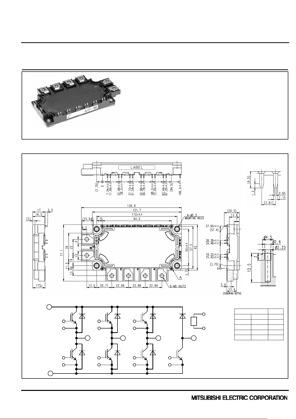
<IGBT Modules>
CM100RX-24S1
INSULATED TYPE
Publication Date : September 2017
CMH-10249-B
Ver.1.3
sevenpack (3φ Inverter + Brake Chopper)
OUTLINE DRAWING & INTERNAL CONNECTION
Dimension in mm
TERMINAL
SECTION A
GWP(12)
W(3)
EWP(11)
NTC
TH1(7)
TH2(8)
GWN(10)
EWN(9)
GVP(16)
V(2)
EVP(15)
GVN(14)
EVN(13)
GUP(20)
U(1)
EUP(19)
GUN(18)
EUN(17)
P(21)
N(22)
B(4)
GB(6)
EB(5)
0.5
to 3
±0.2
HIGH POWER SWITCHING USE
CM100RX-24S1
HIGH POWER SWITCHING USE
INSULA TED TYPE
APPLICATION
AC Motor Control, Motion/Servo Control, etc.
Collector current IC .............…..............................… 1 0 0 A
Collector-emitter voltage V
Maximum junction temperature T
..............................… 1 2 0 0 V
CES
........................ 1 7 5 °C
jmax
●Flat base Type
●Copper base plate (non-plating)
●Tin plating pin terminals
●RoHS Directive* compliant
●Recognized under UL1557, File E323585
t=0.8
INTERNAL CONNECTION
Tolerance otherwise specified
Division of Dimension Tolerance
over 3 to 6 ±0.3
over 6 to 30 ±0.5
over 30 to 120 ±0.8
over 120 to 400 ±1.2
1
<IGBT Modules>
CM100RX-24S1
INSULATED TYPE
Publication Date : September 2017
CMH-10249-B
Ver.1.3
Symbol
Item
Conditions
Rating
Unit
V
Collector-emitter voltage
G-E short-circuited
1200
V
V
Gate-emitter voltage
C-E short-circuited
± 20
V IC
DC, TC=107 °C
100
I
Pulse, Repetitive
200
P
Total power dissipation
TC=25 °C
625
W
IE
DC
100
I
Pulse, Repetitive
200
Symbol
Item
Conditions
Rating
Unit
V
Collector-emitter voltage
G-E short-circuited
1200
V V
Gate-emitter voltage
C-E short-circuited
± 20
V IC
DC, TC=113 °C
50
I
Pulse, Repetitive
100
P
Total power dissipation
TC=25 °C
340
W
V
RRM
Repetitive peak reverse voltage
G-E short-circuited
1200
V
IF
DC
50
I
Pulse, Repetitive
(Note3)
100
Symbol
Item
Conditions
Rating
Unit
V
Isolation voltage
Terminals to base plate, RMS, f=6 0 Hz , AC 1 min
4000
V T
Maximum junction temperature
Instantaneous event (overload)
175
T
Maximum case temperature
(Note4)
125
T
jop
Operating junction temperature
Continuous operation (under switching)
-40 ~ +150
T
Storage temperature
-
-40 ~ +125
Limits
Min.
Typ.
Max.
I
Collector-emitter cut-off current
VCE=V
, G-E short-circuited
- - 1.0
mA
I
Gate-emitter leakage current
VGE=V
, C-E short-circuited
- - 0.5
μA
V
GE(th)
Gate-emitter threshold voltage
IC=10 mA, VCE=10 V
5.4
6.0
6.6
V
IC=100 A, VGE=15 V,
Tj=25 °C
-
1.80
2.25
Refer to the figure of test circuit
Tj=125 °C
-
2.00
-
Tj=150 °C
-
2.05
-
IC=100 A,
Tj=25 °C
-
1.70
2.15
VGE=15 V,
Tj=125 °C
-
1.90
-
Tj=150 °C
-
1.95
- C
Input capacitance
- - 10
C
oes
Output capacitance
- - 2.0
C
Reverse transfer capacitance
- - 0.17
QG
Gate charge
VCC=600 V, IC=100 A, VGE=15 V
-
210 - nC t
Turn-on delay time
- - 300
tr
Rise time
- - 200
t
Turn-off delay time
- - 600
tf
Fall time - -
300
HIGH POWER SWITCHING USE
MAXI MUM RATINGS (Tj=25 °C, unless otherwise specified)
INVERTER PART IGBT/DIODE
CES
GES
(Note1)
(Note1)
Collector current
(Note2)
Emitter current
Collector current
CRM
tot
ERM
BRAKE PART IGBT/DIODE
CES
GES
CRM
tot
(Note2, 4)
(Note2, 4)
(Note2, 4)
(Note3)
(Note3)
(Note2, 4)
(Note3)
A
A
A
(Note2)
FRM
Forward current
MODULE
isol
jmax
Cmax
stg
ELECTRICAL CHARACTERISTICS (Tj=25 °C, unless otherwise specified)
INVERTER PART IGBT/DIODE
Symbol Item Conditions
CES
GES
V
CE sat
(Terminal)
V
CE sat
(Chip)
ies
res
Collector-emitter saturation voltage
CES
GES
(Note5)
(Note5)
VCE=10 V, G-E short-circuited
A
°C
°C
Unit
V
V
nF
d(on)
d(off)
VCC=600 V, IC=100 A, VGE=±15 V,
ns
RG=6.2 Ω, Inductive load
2
<IGBT Modules>
CM100RX-24S1
INSULATED TYPE
Publication Date : September 2017
CMH-10249-B
Ver.1.3
Limits
Min.
Typ.
Max.
IE=100 A, G-E short-circuited,
Tj=25 °C
-
2.60
3.40
Refer to the figure of test circuit
Tj=125 °C
-
2.16
-
Tj=150 °C
-
2.10
-
IE=100 A,
Tj=25 °C
-
2.50
3.30
G-E short-circuited,
Tj=125 °C
-
2.06
-
Tj=150 °C
-
2.00
- trr
Reverse recovery time
VCC=600 V, IE=100 A, VGE=±15 V,
- - 300
ns
Qrr
(Note1)
Reverse recovery charge
RG=6.2 Ω, Inductive load
-
2.7 - μC
Eon
Turn-on s witching energy per pulse
VCC=600 V, IC=IE=100 A,
-
5.9
-
E
off
Turn-off switching energy per pulse
VGE=±15 V, RG=6.2 Ω, Tj=150 °C,
-
9.7
- Err
Reverse recovery energy per pulse
Inductive load
-
9.7 - mJ
Main terminals-chip, per switch,
TC=25 °C
rg
Internal gate resistance
Per switch
- 0 -
Ω
Limits
Min.
Typ.
Max.
I
Collector-emitter cut-off current
VCE=V
, G-E short-circuited
- - 1.0
mA
I
Gate-emitter leakage current
VGE=V
, C-E short-circuited
- - 0.5
μA V
GE(th)
Gate-emitter threshold voltage
IC=5 mA, VCE=10 V
5.4
6.0
6.6
V
IC=50 A, VGE=15 V,
Tj=25 °C
-
1.80
2.25
Refer to the figure of test circuit
Tj=125 °C
-
2.00
-
Tj=150 °C
-
2.05
-
IC=50 A,
Tj=25 °C
-
1.70
2.15
VGE=15 V,
Tj=125 °C
-
1.90
-
Tj=150 °C
-
1.95
-
C
Input capacitance
- - 5.0
C
oes
Output capacitance
- - 1.0
C
Reverse transfer capacitance
- - 0.08
QG
Gate charge
VCC=600 V, IC=50 A, VGE=15 V
-
105 - nC
t
Turn-on delay time
- - 300
tr
Rise time
- - 200
t
Turn-off delay time
- - 600
tf
Fall time - -
300
I
Repetitive peak reverse current
VR=V
, G-E short-circuited
- - 1.0
mA
IE=50 A, G-E short-circuited,
Tj=25 °C
-
2.60
3.40
Refer to the figure of test circuit
Tj=125 °C
-
2.16
-
Tj=150 °C
-
2.10
-
IE=50 A,
Tj=25 °C
-
2.50
3.30
G-E short-circuited,
Tj=125 °C
-
2.06
-
Tj=150 °C
-
2.00
- trr
Reverse recovery time
VCC=600 V, IE=50 A, VGE=±15 V,
- - 300
ns
Qrr
Reverse recovery charge
RG=13 Ω, Inductive load
-
1.3 - μC Eon
Turn-on s witching energy per pulse
VCC=600 V, IC=IE=50 A,
-
3.2
-
E
Turn-off switching energy per pulse
VGE=±15 V, RG=13 Ω, Tj=150 °C,
-
5.0
- Err
Reverse recovery energy per pulse
Inductive load
-
4.4 - mJ
rg
Internal gate resistance
- - 0 - Ω
HIGH POWER SWITCHING USE
ELECTRICAL CHARACTERISTICS (cont.; Tj=25 °C, unless otherwise specified)
INVERTER PART IGBT/DIODE
Symbol Item Conditions
(Note1)
VEC
(Terminal)
(Note5)
Emitter-collector voltage
(Note1)
VEC
(Chip)
(Note1)
(Note1)
R
Internal lead resistance
CC'+EE'
(Note5)
(Note4)
BRAKE PART IGBT/DIODE
Symbol Item Conditions
CES
GES
V
CE sat
(Terminal)
V
CE sat
(Chip)
ies
res
Collector-emitter saturation voltage
CES
GES
(Note5)
(Note5)
VCE=10 V, G-E short-circuited
Unit
V
V
mJ
- - 0.8 mΩ
Unit
V
V
nF
d(on)
d(off)
RRM
V
F
(Terminal)
VCC=600 V, IC=50 A, VGE=±15 V,
ns
RG=13 Ω, Inductive load
RRM
V
(Note5)
Forward voltage
V
F
(Chip)
off
(Note5)
V
mJ
3
<IGBT Modules>
CM100RX-24S1
INSULATED TYPE
Publication Date : September 2017
CMH-10249-B
Ver.1.3
Limits
Min.
Typ.
Max.
R25
Zero-power resistance
TC=25 °C
4.85
5.00
5.15
kΩ ΔR/R
Deviation of resistance
R
=493 Ω, TC=100 °C
-7.3 - +7.8
% B
B-constant
Approximate by equation
-
3375 - K
P25
Power dissipation
TC=25 °C
- - 10
mW
Limits
Min.
Typ.
Max.
R
th(j- c)Q
Junction to case, per Inverter IGBT
- - 0.24
R
Junction to case, per Inverter DIODE
- - 0.37
R
Junction to case, per Brake IGBT
- - 0.44
R
th(j- c)D
Junction to case, per Brake DIODE
- - 0.66
Case to heat sink, per 1 module,
Thermal grease applied
(Note4, 7)
Limits
Min.
Typ.
Max.
Mt
Mounting torque
Main terminals
M 5 screw
2.5
3.0
3.5
N·m
Ms
Mounting torque
Mounting to heat sink
M 5 screw
2.5
3.0
3.5
N·m
Terminal to terminal
17 - -
Terminal to base plate
20.1 - -
Terminal to terminal
10 - -
Terminal to base plate
14.8 - -
m
mass - -
370 - g
ec
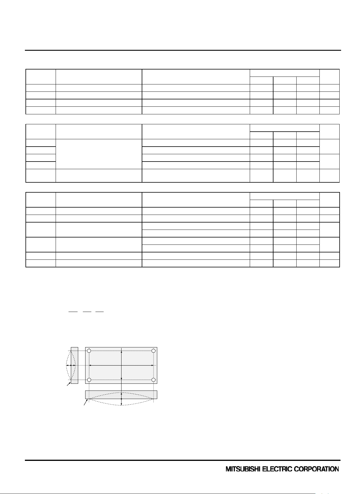
Flatness of base plate
On the centerline X, Y
±0 - +100
μm
)
TT
/()
R
R
ln(B
)/(
502550
25
5025
11
−=
Y
X
+:Convex
-:Concave
+:Convex
-:Concave
mounting side
mounting side
mounting side
HIGH POWER SWITCHING USE
ELECTRICAL CHARACTERISTICS (cont.; Tj=25 °C, unless otherwise specified)
NTC THERMISTOR P ART
Symbol Item Conditions
(Note4)
100
(25/50)
(Note4)
THERMAL RESISTANCE CHARACTERISTICS
Symbol Item Conditions
th(j- c)D
th(j- c)Q
R
th(c- s )
Thermal resistance
Contact thermal resistance
MECHANICAL CHARACTERISTICS
Symbol Item Conditions
ds Creepage distance
da Clearance
(Note4)
(Note6)
(Note4)
(Note4)
(Note4)
(Note4)
Unit
Unit
K/W
K/W
- 15 - K/kW
Unit
mm
mm
(Note8)
Note1. Represent ratings and characteristics of the anti-parallel, emitter-collector free wheeling diode (DIODE).
2. Junction temperature (T
) should not increase beyond T
j
3. Pulse width and repetition rate should be such that the device junction temperature (T
4. Case temperature (T
) and heat sink temperature (Ts) are defined on the each surface (mounting side) of base plate and heat sink
C
jmax
rating.
) dose not exceed T
j
jmax
rating.
just under the chips. Refer to the figure of chip location.
5. Pulse width and repetition rate should be such as to cause negligible temperature rise.
6.
: resistance at absolute temperature T25 [K]; T25=25 [°C]+273.15=298.15 [K]
R
25
: resistance at absolute temperature T50 [K]; T50=50 [°C]+273.15=323.15 [K]
R
50
,
7. Typical value is measured by using thermally conductive grease of λ=0.9 W/(m·K).
8. The base plate (mounting side) flatness measurement points (X, Y) are as follows of the following figure.
4

<IGBT Modules>
CM100RX-24S1
INSULATED TYPE
Publication Date : September 2017
CMH-10249-B
Ver.1.3
9.
Use the following screws when mounting the printed circuit board (PCB) on the standoffs.
PT
Limits
Min.
Typ.
Max.
VCC
(DC) Supply voltage
Applied across P-N terminals
-
600
850
V
Applied across GB-EB/
G*P-E*P/G*N-E*N(*=U, V, W) terminals
Inverter IGBT
6.2 - 62
Brake IGBT
13 - 130
HIGH POWER SWITCHING USE
PCB thickness : t=1.6.
Type Size Tightening torque Recommended tightening method
(1)
(2)
(3)
(4)
(5) B1 tapping screw φ2.6×10 or φ2.6×12
PT
DELTA PT
DELTA PT
K25×8
K25×10
25×8
25×10
* This product is compliant with the Restriction of the Use of Certain Hazardous Substances in Electrical and Electronic Equipment (RoHS).
RECOMMENDED OPERATING CONDITIONS
Symbol Item Conditions
V
Gate (-emitter drive) voltage
GEon
RG External gate resistance Per switch
0.55 ± 0.055 N・m
0.75 ± 0.075 N・m
0.55 ± 0.055 N・m
0.75 ± 0.075 N・m
0.75 ± 0.075 N・m
by handwork (equivalent to 30 rpm
by mechanical screw driver)
~ 600 rpm (by mechanical screw driver)
Unit
13.5 15.0 16.5 V
Ω
5

<IGBT Modules>
CM100RX-24S1
INSULATED TYPE
Publication Date : September 2017
CMH-10249-B
Ver.1.3
CHIP LOCATION (Top view)
Dimension in mm, tolerance: ±1 mm
Tr*P/Tr*N/TrBr: IGBT, Di*P/Di*N: DIODE (*=U/V/W), DiBr: Brake DIODE, Th: NTC thermistor
VCC
-VGE
+VGE
-VGE
+
vCE
vGE
0
iE
iC
P
N
*
G*P
E*P
G*N
E*N
Load
RG
*: U, V, W
~
t
tf
tr
t
d(on)
iC
10%
90 %
90 %
vGE
~
~
~
0 V
0 A
0
t
d(off)
t
Irr
Qrr=0.5×Irr×trr
0.5×Irr
t
trr
iE
0 A
IE
0.1×ICM
ICM
VCC
vCE
iC
t
0
ti
0.1×VCC
0.1×VCC
VCC
ICM
vCE
iC
t
0
0.02×ICM
ti
IEM
vEC
i
E
t
0 V
ti
t
VCC
0 A
IGBT T urn-on switching energy
IGBT T urn-off switching energy
DIODE Reverse recovery energy
HIGH POWER SWITCHING USE
TEST CIRCUIT AND WAVEFORMS
Switching test circuit and waveforms trr, Qrr test waveform
Turn-on / Turn-off switching energy and Reverse recovery energy test waveforms (Integral time instruction drawing)
6

<IGBT Modules>
CM100RX-24S1
INSULATED TYPE
Publication Date : September 2017
CMH-10249-B
Ver.1.3
V
G-E short-
circuited
21
1
22
IC
20
19
18
17
VGE=15V
V
G-E short-
circuited
21
2
22
IC
16
15
14
13
VGE=15V
V
G-E short-
circuited
21
3
22
IC
12
11
10
9
VGE=15V
VGE=15V
G-E short-
circuited
21
1
22
IC
20
19
18
17
V
VGE=15V
G-E short-
circuited
21
2
22
IC
16
15
14
13
V
VGE=15V
G-E short-
circuited
21
3
22
IC
12
11
10
9
V
VGE=15V
21
4
22
IC
6
5
V
Gate-emitter
GVP-EVP GVN-EVN,
GB-EB
Gate-emitter
GUP-EUP, GUN-EUN,
GB-EB
Gate-emitter
GUP-EUP, GUN-EUN,
GB-EB
Gate-emitter
GUP-EUP, GUN-EUN,
GWP-EW P, GW N-EWN
V
G-E short-
circuited
21
1
22
IE
20
19
18
17
G-E short
-
circuited
V
G-E short
-
circuited
21
2
22
IE
16
15
14
13
G-E short-
circuited
V
G-E short-
circuited
21
3
22
IE
12
11
10
9
G
-E shortcircuited
G-E short-
circuited
21
1
22
IE
20
19
18
17
V
G-E short-
circuited
G-E short-
circuited
21
2
22
IE
16
15
14
13
V
G-E short-
circuited
G-E short-
circuited
21
3
22
IE
12
11
10
9
V
G-E short-
circuited
21
4
22
IE
6
5
V
G-E short-
circuited
Gate-emitter
GVP-EVP GVN-EVN,
GB-EB
Gate-emitter
GUP-EUP, GUN-EUN,
GB-EB
Gate-emitter
GUP-EUP, GUN-EUN,
GB-EB
Gate-emitter
GUP-EUP, GUN-EUN,
GWP-EW P, GW N-EWN
UP / UN DIODE
VP / VN DIODE
WP / WN DIODE
Brake DIODE
HIGH POWER SWITCHING USE
TEST CIRCUIT
short-circuited
GWP-EW P, GW N-EWN,
UP / UN IGBT
short-circuited
GWP-EWP, GWN-EWN,
VP / VN IGBT
V
characteristics test circuit
CEsat
short-circuited
GVP-EVP, GVN-EVN,
WP / WN IGBT
short-circuited
GVP-EVP, GVN-EVN,
Brake IGBT
short-circuited
GWP-EW P, GW N-EWN,
short-circuited
GWP-EWP, GWN-EWN,
short-circuited
VEC / VF characteristics test circuit
7
GVP-EVP, GVN-EVN,
short-circuited
GVP-EVP, GVN-EVN,

<IGBT Modules>
CM100RX-24S1
INSULATED TYPE
Publication Date : September 2017
CMH-10249-B
Ver.1.3
OUTPUT
COLLECTOR-EMITTER SATURATION VO LTAG E
CHARACTERISTICS
CHARACTERISTICS
(TYPICAL)
(TYPICAL)
Tj=25 °C
(Chip)
VGE=15 V
(Chip)
COLLECTOR CURRENT I
C
(A)
0
50
100
150
200
0 2 4
6 8 10
COLLECTOR-EMITTER SATURATION VO LTAG E V
CEsat
(V)
0
0.5
1
1.5
2
2.5
3
3.5
0 50 100 150 200
COLLECTOR-EMITTER VOLTAGE VCE (V)
COLLECTOR CURRENT IC (A)
COLLECTOR-EMITTER SATURATION VOLTAGE
FREE WHEELING DIODE
CHARACTERISTICS
FORWARD CHARACTERISTICS
(TYPICAL)
(TYPICAL)
Tj=25 °C
(Chip)
G-E short-circuited
(Chip)
COLLECTOR-EMITTER SATURATION VO LTAG E V
CEsat
(V)
0
2
4
6
8
10
6 8 10 12 14 16 18 20
EMITTER CURRENT I
E
(A)
10
100
1000
0.5 1 1.5 2 2.5 3 3.5 4
GATE-EMITTER VOLTAGE VGE (V)
EMITTER-COLLECTOR VOLTAGE VEC (V)
Tj=150 °C
Tj=125 °C
Tj=25 °C
Tj=125 °C
Tj=25 °C
IC=200 A
IC=100 A
IC=40 A
Tj=150 °C
HIGH POWER SWITCHING USE
PERFORMANCE CURVES
INVERTER PART
VGE=20 V
15 V
12 V
11 V
10 V
9 V
8

<IGBT Modules>
CM100RX-24S1
INSULATED TYPE
Publication Date : September 2017
CMH-10249-B
Ver.1.3
HALF-BRIDGE
HALF-BRIDGE
SWITCHING CHARACTERISTICS
SWITCHING CHARACTERISTICS
(TYPICAL)
(TYPICAL)
VCC=600 V, VGE=±15 V, RG=6.2 Ω, INDUCTIVE LOAD
VCC=600 V, VGE=±15 V, IC=100 A, INDUCTIVE LOAD
---------------: Tj=150 °C, - - - - -: Tj=125 °C
---------------: Tj=150 °C, - - - - -: Tj=125 °C
SWITCHING TIME (ns)
1
10
100
1000
10 100 1000
SWITCHING TIME (ns)
10
100
1000
1 10 100
COLLECTOR CURRENT IC (A)
EXTERNAL GATE RESISTANCE RG (Ω)
HALF-BRIDGE
HALF-BRIDGE
SWITCHING CHARACTERISTICS
SWITCHING CHARACTERISTICS
(TYPICAL)
(TYPICAL)
VCC=600 V, VGE=±15 V, RG=6.2 Ω,
VCC=600 V, VGE=±15 V, IC/IE=100 A,
INDUCTIVE LOAD, PER PULSE
INDUCTIVE LOAD, PER PULSE
---------------: Tj=150 °C, - - - - -: Tj=125 °C
---------------: Tj=150 °C, - - - - -: Tj=125 °C
SWITCHING ENERGY (mJ)
0.1
1
10
10 100 1000
1
10
100
REVERSE RECOVERY ENERGY (mJ)
SWITCHING ENERGY (mJ)
REVERSE RECOVERY ENERGY (mJ)
1
10
100
1 10 100
COLLECTOR CURRENT IC (A)
EXTERNAL GATE RESISTANCE RG (Ω)
EMITTER CURRENT IE (A)
tf
tr
tf
Err
HIGH POWER SWITCHING USE
PERFORMANCE CURVES
INVERTER PART
t
d(off)
t
tr
d(on)
t
d(off)
t
d(on)
E
off
Eon
Eon
E
off
Err
9
<IGBT Modules>
CM100RX-24S1
INSULATED TYPE
Publication Date : September 2017
CMH-10249-B
Ver.1.3
CAPACITANCE
FREE WHEELING DIODE
CHARACTERISTICS
REVERSE RECOVERY CHARACTERISTICS
(TYPICAL)
(TYPICAL)
VCC=600 V, VGE=±15 V, RG=6.2 Ω, INDUCTIVE LOAD
G-E short-circuited, Tj=25 °C
---------------: Tj=150 °C, - - - - -: Tj=125 °C
CAPACITANCE (nF)
0.01
0.1
1
10
100
0.1 1 10 100
t
rr
(ns), I
rr
(A)
10
100
1000
10 100 1000
COLLECTOR-EMITTER VOLTAGE VCE (V)
EMITTER CURRENT IE (A)
GATE CHARGE
CHARACTERISTICS
TRANSIENT THERMAL IMPEDANCE
(TYPICAL)
CHARACTERISTICS
(MAXIMUM)
Single pulse, TC=25 °C
VCC=600 V, IC=100 A, Tj=25 °C
R
th(j- c)Q
=0.24 K/W, R
th(j-c)D
=0.37 K/W
GATE-EMITTER VOLTAGE V
GE
(V)
0
5
10
15
20
0 50 100 150 200 250 300
NORMALIZED TR ANSIENT THERMAL RESISTANCE Z
th(j-c)
0.001
0.01
0.1
1
0.00001 0.0001 0.001 0.01 0.1 1 10
GATE CHARGE QG (nC)
TIME (S)
Irr
C
HIGH POWER SWITCHING USE
PERFORMANCE CURVES
INVERTER PART
C
ies
oes
trr
C
res
10

<IGBT Modules>
CM100RX-24S1
INSULATED TYPE
Publication Date : September 2017
CMH-10249-B
Ver.1.3
COLLECTOR-EMITTER SATURATION
CLAMP DIODE
VOLTAGE CHARACTERISTICS
FORWARD CHARACTERISTICS
(TYPICAL)
(TYPICAL)
VGE=15 V
(Chip)
G-E short-circuited
(Chip)
COLLECTOR-EMITTER SATURATION VOLTAGE V
CEsat
(V)
0
0.5
1
1.5
2
2.5
3
3.5
0 20 40 60
80 100
FORWARD VOLTAGE V
F
(V)
10
100
1000
0.5 1 1.5 2 2.5 3 3.5 4
COLLECTOR CURRENT IC (A)
FORWARD CURRENT IF (A)
HALF-BRIDGE
HALF-BRIDGE
SWITCHING CHARACTERISTICS
SWITCHING CHARACTERISTICS
(TYPICAL)
(TYPICAL)
VCC=600 V, VGE=±15 V, RG=13 Ω, INDUCTIVE LOAD
VCC=600 V, IC=50 A, VGE=±15 V, INDUCTIVE LOAD
---------------: Tj=150 °C, - - - - -: Tj=125 °C
---------------: Tj=150 °C, - - - - -: Tj=125 °C
SWITCHING TIME (ns)
1
10
100
1000
1 10 100
SWITCHING TIME (ns)
10
100
1000
10 100 1000
COLLECTOR CURRENT IC (A)
EXTERNAL GATE RESISTANCE RG (Ω)
Tj=150 °C
Tj=125 °C
Tj=25 °C
Tj=150 °C
Tj=25 °C
tf
Tj=125 °C
HIGH POWER SWITCHING USE
PERFORMANCE CURVES
BRAKE PART
t
d(off)
t
d(off)
tf
t
d(on)
t
d(on)
tr
t
r
11

<IGBT Modules>
CM100RX-24S1
INSULATED TYPE
Publication Date : September 2017
CMH-10249-B
Ver.1.3
HALF-BRIDGE
HALF-BRIDGE
SWITCHING CHARACTERISTICS
SWITCHING CHARACTERISTICS
(TYPICAL)
(TYPICAL)
VCC=600 V, VGE=±15 V, RG=13 Ω,
VCC=600 V, IC/IF=50 A, VGE=±15 V,
INDUCTIVE LOAD, PER PULSE
INDUCTIVE LOAD, PER PULSE
---------------: Tj=150 °C, - - - - -: Tj=125 °C
---------------: Tj=150 °C, - - - - -: Tj=125 °C
SWITCHING ENERGY (mJ)
0.01
0.1
1
10
1 10 100
0.1
1
10
100
REVERSE RECOVERY ENERGY (mJ)
SWITCHING ENERGY (mJ)
REVERSE RECOVERY ENERGY (mJ)
1
10
100
10 100 1000
COLLECTOR CURRENT IC (A)
EXTERNAL GATE RESISTANCE RG (Ω)
FORWARD CURRENT IF (A)
BRAKE DIODE
TRANSIENT THERMAL IMPEDANCE CHARACTERISTICS
REVERSE RECOVERY CHARACTERISTICS
(TYPICAL)
(MAXIMUM)
VCC=600 V, VGE=±15 V, RG=13 Ω, INDUCTIVE LOAD
Single pulse, TC=25 °C
---------------: Tj=150 °C, - - - - -: Tj=125 °C
R
=0.44 K/W, R
=0.66 K/W
t
rr
(ns), I
rr
(A)
10
100
1000
1 10 100
NORMALIZED TR ANSIENT THERMAL RESISTANCE Z
th(j-c)
0.001
0.01
0.1
1
0.00001 0.0001 0.001 0.01 0.1 1 10
FORWARD CURRENT IF (A)
TIME (S)
trr
HIGH POWER SWITCHING USE
PERFORMANCE CURVES
BRAKE PART
E
off
E
on
Err
Eon
E
off
Err
th(j- c)Q
th(j-c)D
Irr
12

<IGBT Modules>
CM100RX-24S1
INSULATED TYPE
Publication Date : September 2017
CMH-10249-B
Ver.1.3
TEMPERATURE
CHARACTERISTICS
(TYPICAL)
RESISTANCE R (kΩ)
0.1
1
10
100
-50 -25 0 25 50 75 100 125
TEMPERATURE T (°C)
HIGH POWER SWITCHING USE
PERFORMANCE CURVES
NTC thermistor part
13

<IGBT Modules>
CM100RX-24S1
INSULATED TYPE
Publication Date : September 2017
CMH-10249-B
Ver.1.3
HIGH POWER SWITCHING USE
Keep safety first in your cir c uit des igns!
This product is designed for industrial application purpose. The performance, the quality and support level of the product is
guaranteed by “Customer's Std. Spec.”.
Mitsubishi Electric Cor porat ion put s it s rea sonable eff ort int o making s emicondu ctor pr oducts better and more reliable, but there
is always the possibility that trouble may occur with them by the reliability lifetime such as Power Cycle, Thermal Cycle or
others, or to be used under special circumstances(e.g. high humidity, dusty, salty, highlands, environment with lots of organic
matter / corrosive gas / explosive gas, or situation which terminal of semiconductor products is received strong mechanical
stress).
In the customer's research and development, please evaluate it not only with a single semiconductor product but also in the
entire system, and judge whether it's applicable. Furthermore, trouble with semiconductors may l ead to personal injury, fire or
property damage. Remember to give due consideration to safety when making your circuit designs, with appropriate measures
such as (i) placement of substitutive, auxiliary circuits (e.g. appropriate fuse or circuit breaker between a power supply and
semiconductor products), (ii) use of non-flammable material or (iii) prevention against any malfunction or mishap.
Notes regarding these ma t er ials
•These materials are intended as a reference to assist our customers in the selection of the Mitsubishi semiconductor product
best suited to the custom er's application; they do not convey any lic ense under any intellectual property rights, or any other
rights, belonging to Mitsubishi Electric Corporation or a third party.
•Mitsubishi Electri c Corp oratio n assu mes no r espon sibility f or any damage , or infringe ment of any third-p ar ty's r ight s, ori ginat ing
in the use of any product data, diagrams, charts, or circuit application examples contained in thes e materials.
•All information cont ai ned in these materials, including product da t a, d iagr am s an d ch arts represents information on prod ucts at
the time of publication of these materials, and are subject to change by Mitsubishi Electric Corporation without notice due to
product improvement s or other reasons. It is therefore recommend ed t hat cu sto mers co nt act Mitsubishi Electric Corporatio n or
an authorized Mit subishi Semi conduct or pro duct d istribut or f or the latest prod uct inf ormatio n bef ore pur chasing a pr oduct listed
herein.
The information described here may contain technical inaccurac ies or typographical errors. Mitsubishi Electric Corporation
assumes no responsibili ty for any damage, liability, or other loss rising from these inaccuracies or errors.
Please also pay attention to information published by Mitsubishi Electric Corporation by various means, including the
Mitsubishi Semiconductor home page (www.MitsubishiElectric.com/semiconductors/).
•When using any or all of the information contained in these materials, including product data, diagrams, and charts, please be
sure to evaluate all information as a total system before making a final decis ion on the applicability of the information and
products. Mits ubishi Electric Corporation assumes no responsibility for any damage, liability or ot her loss resulti ng from the
information contained herein.
•Mitsubishi Electric Corporation semiconductors are not designed or manufactured for use in a device or system that is used
under circumstances in which human life is potentially at stake. Therefore, this product should not be used in such
applications.
Please contact M itsubis hi Elec tric Corpor ati on or an author iz ed M itsubis hi Semic onductor p roduct distribu tor w hen consid ering
the use of a product contained herein for any specific purposes, such as apparatus or systems for transportation, vehicular,
medical, aerospace, nuclear, or undersea repeater use.
•In the case of new requirement is available, this material will be revised upon consultation.
•The prior written approval of Mitsubishi Electric Corporation is necessary to reprint or reproduce in whole or in part these
materials.
•If these product s or tec hnologies are subject to the Japa ne s e export control restrictions, they mu st be exported under a license
from the Japanese government and cannot be imported into a country other than the approved destination.
Any diversion or re-export contrary to the export control laws and regulations of Japan and/or the country of destination is
prohibited.
•Please contact Mitsubishi Electric Corporation or an authorized Mitsubishi Semiconductor product distributor for further details
on these materials or the products contained therein.
Generally the listed company name and the brand name are the trademarks or registered trademarks of the respective companies.
© 2017 MITSUBISHI ELECTRIC CORPORATION. ALL RIGHTS RESERVED
14
 Loading...