

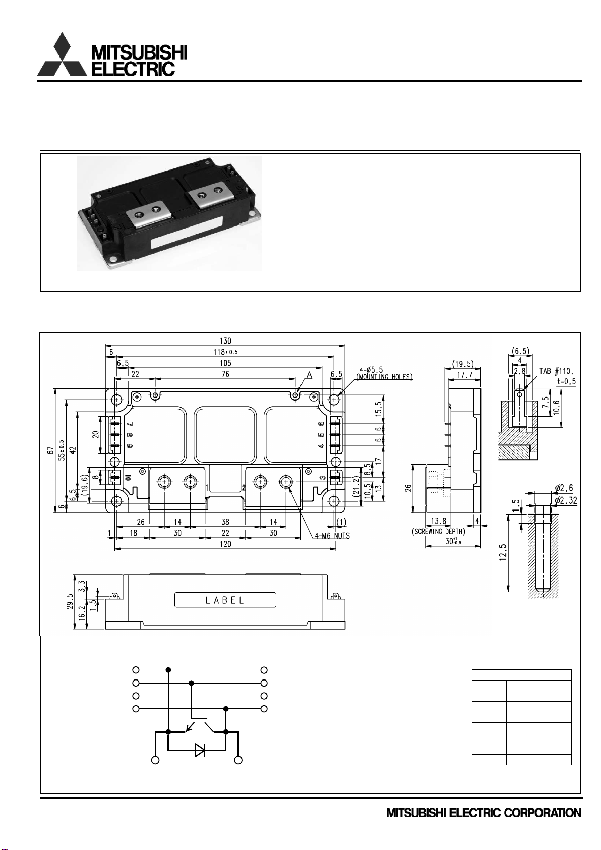
Mitsubishi Electric US, Inc CM1000HA-34S Data Sheet
<IGBT Modules>
Publication Date : September 2016
1
CMH-11148
Ver.1.0
Collector current IC .............…..................…
1 0 0
0
A
Collector-emitter voltage V
CES
..................
1 7 0
0
V
Maximum junction temperature T
vjmax
.........
1 7
5
°C
●Flat base Type
●Copper base plate
●Tin plating tab terminals
●RoHS Directive compliant
single pack
●Recognized under UL1557, File E323585
APPLICATION
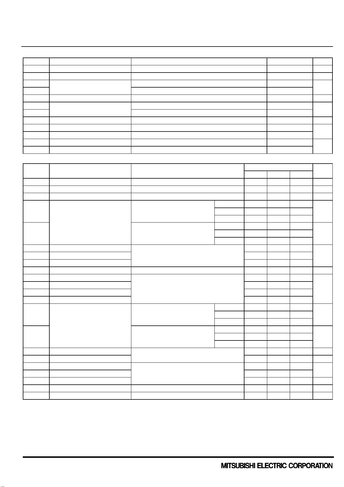
OUTLINE DRAWING & INTERNAL CONNECTION
Dimension in mm
TERMINAL
SECTION A
INTERNAL CONNECTION
Terminal code
2
1
4
5 6 9
8
7 3 10
Tr
Di
1: E
2: C
3: CS
4: NC
5: G
6: ES
7: ES
8: G
9: NC
10: CS
Tolerance otherwise specified
Division of Dimension
Tolerance
0.5
to 3
±0.2 over 3
to 6
±0.3 over 6
to 30
±0.5 over 30
to 120
±0.8
over 120
to 400
±1.2
over 400
to 1000
±2.0
over 1000
to 2000
±3.0
over 2000
to 4000
±4.0
CM1000HA-34S
HIGH POWER SWITCHING USE
INSULATED TYPE
AC Motor Control, Motion/Servo Control, Power supply, Photovoltaic power, Wind power, etc.
<IGBT Modules>
CM1000HA-34S
HIGH POWER SWITCHING USE
INSULATED TYPE
Publication Date : September 2016
2
CMH-11148
Ver.1.0
Symbol
Item
Conditions
Rating
Unit
V
CES
Collector-emitter voltage
G-E short-circuited
1700
V V
GES
Gate-emitter voltage
C-E short-circuited
± 20
V IC
Collector current
DC, TC=111 °C
(Note2, 4)
1000
A
I
CRM
Pulse, Repetitive
(Note3)
2000
P
tot
Total power dissipation
TC=25 °C
(Note2, 4)
7140
W IE
(Note1)
Emitter current
DC
(Note2)
1000
A
I
ERM
(Note1)
Pulse, Repetitive
(Note3)
2000
V
is o l
Isolation voltage
Terminals to base plate, RMS, f=60 Hz, AC 1 min
4000
V
T
vjmax
Maximum junction temperature
Instantaneous event (overload)
175
°C
T
Cm a x
Maximum case temperature
(Note4)
125
T
vjop
Operating junction temperature
Continuous operation (under switching)
-40 ~ +150
°C
T
st g
Storage temperature
-
-40 ~ +125
Symbol
Item
Conditions
Limits
Unit
Min.
Typ.
Max.
I
CE S
Collector-emitter cut-off current
VCE=V
CES
, G-E short-circuited
- - 1.0
mA
I
GE S
Gate-emitter leakage current
VGE=V
GES
, C-E short-circuited
- - 0.5
μA V
GE (th)
Gate-emitter threshold voltage
IC=100 mA, VCE=10 V
5.4
6.0
6.6
V
V
CE sat
(Terminal)
Collector-emitter saturation voltage
IC=1000 A, VGE=15 V,
Tvj=25 °C
-
2.10
2.60
Refer to the figure of test circuit
Tvj=125 °C
-
2.35 - V
(Note5)
Tvj=150 °C
-
2.45 -
V
CE sat
(Chip)
IC=1000 A,
Tvj=25 °C
-
2.00
2.50
VGE=15 V,
Tvj=125 °C
-
2.25 - V
(Note5)
Tvj=150 °C
-
2.35 -
C
ies
Input capacitance
- -
230
C
oe s
Output capacitance
VCE=10 V, G-E short-circuited
- - 24
nF
C
re s
Reverse transfer capacitance
- -
4.0
QG
Gate charge
VCC=1000 V, IC=1000 A, VGE=15 V
-
4.2 - μC
t
d( o n)
Turn-on delay time
VCC=1000 V, IC=1000 A, VGE=±15 V,
- - 900
tr
Rise time
- - 300
ns
t
d( o ff )
Turn-off delay time
RG=0 Ω, Inductive load
- - 900
tf
Fall time - -
400
VEC
(Note.1)
(Terminal)
Emitter-collector voltage
IE=1000 A, G-E short-circuited,
Tvj=25 °C
-
2.10
2.60
Refer to the figure of test circuit
Tvj=125 °C
-
2.20 - V
(Note5)
Tvj=150 °C
-
2.15 -
VEC
(Note.1)
(Chip)
IE=1000 A,
Tvj=25 °C
-
2.00
2.50
G-E short-circuited,
Tvj=125 °C
-
2.10 - V
(Note5)
Tvj=150 °C
-
2.05 -
t
rr
(Note1)
Reverse recovery time
VCC=1000 V, IE=1000 A, VGE=±15 V,
- - 500
ns
Qrr
(Note1)
Reverse recovery charge
RG=0 Ω, Inductive load
-
200 - μC
Eon
Turn-on switching energy per pulse
VCC=1000 V, IC=IE=1000 A,
-
589
-
mJ
E
off
Turn-off switching energy per pulse
VGE=±15 V, RG=0 Ω, Tvj=150 °C,
-
253
-
Err
(Note1)
Reverse recovery energy per pulse
Inductive load
-
245 - mJ
R
CC'+EE'
Internal lead resistance
Main terminals-chip, TC=25 °C
(Note4)
-
0.2 - mΩ
rg
Internal gate resistance
- - 2.2 - Ω
MAXIMUM RATINGS (Tvj=25 °C, unless otherwise specified)
ELECTRICAL CHARACTERISTICS (Tvj=25 °C, unless otherwise specified)
<IGBT Modules>
CM1000HA-34S
HIGH POWER SWITCHING USE
INSULATED TYPE
Publication Date : September 2016
3
CMH-11148
Ver.1.0
Symbol
Item
Conditions
Limits
Unit
Min.
Typ.
Max.
R
th(j - c ) Q
Thermal resistance
Junction to case, IGBT
(Note4)
- - 21
K/kW
R
th(j - c)D
Junction to case, FWD
(Note4)
- - 32
R
th(c- s )
Contact thermal resistance
Case to heat sink,
-
18 - K/kW
Thermal grease applied
(Note4, 6)
Symbol
Item
Conditions
Limits
Unit
Min.
Typ.
Max.
Mt
Mounting torque
Main terminals
M 6 screw
3.5
4.0
4.5
N·m
Ms
Mounting torque
Mounting to heat sink
M 5 screw
2.5
3.0
3.5
N·m
ds
Creepage distance
Terminal to terminal
22.0 - -
mm
Terminal to base plate
21.9 - -
da
Clearance
Terminal to terminal
16.5 - -
mm
Terminal to base plate
12.5 - -
ec
Flatness of base plate
On the centerline X, Y
(Note7)
-50 - +100
μm
m
mass - -
490 - g
*:
This product is compliant with the Restriction of the Use of Certain Hazardous Substances in Electrical and Electronic Equipment (RoHS) directive 2011/65/EU.
Note1.
Represent ratings and characteristics of the anti-parallel, emitter-collector free-wheeling diode (FWD).
2.
Junction temperature (Tvj) should not exceed T
vjm a x
rating.
3.
Pulse width and repetition rate should be such that the device junction temperature (Tvj) dose not exceed T
vjm a x
rating.
4.
Case temperature (TC) and heat sink temperature (TS) are defined on the each surface (mounting side) of base plate and heat sink just under the chips.
Refer to the figure of chip location.
5.
Pulse width and repetition rate should be such as to cause negligible temperature rise. Refer to the figure of test circuit.
6.
Typical value is measured by using thermally conductive grease of λ=0.9 W/(m·K)/D
(C-S)
=100 μm.
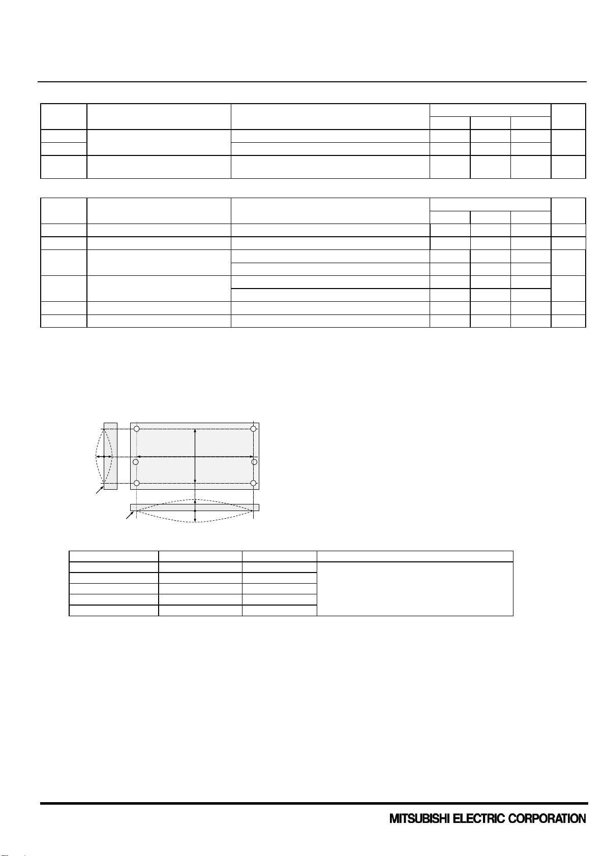
7.
The base plate (mounting side) flatness measurement points (X, Y) are shown in the following figure.
Y
X
+:Convex
-:Concave
+:Convex
-:Concave
Mounting side
Mounting side
Mounting
side
8.
Use the following screws when mounting the printed circuit board (PCB) on the standoffs.
The length of the screw depends on the PCB thickness (t1.0).
Type
Size
Tightening torque
Recommended tightening method
(1)
PT
K25×8
0.55 ± 0.055 N・m
(2)
PT
K25×10
0.85 ± 0.085 N・m
by handwork (equivalent to 30 r/min
(3)
DELTA PT
25×8
0.55 ± 0.055 N・m
by mechanical screw driver)
(4)
DELTA PT
25×10
0.85 ± 0.085 N・m
~ 600 r/min (by mechanical screw driver)
(5)
B1 tapping screw
φ2.6×10 or φ2.6×12
0.85 ± 0.085 N・m
THERMAL RESISTANCE CHARACTERISTICS
MECHANICAL CHARACTERISTICS
 Loading...