


< HVIGBT MODULES >
CM1000E4C-66R
HIGH POWER SWITCHING USE
INSULATED TYPE 4th-Version HVIGBT (High Voltage Insulated Gate Bipolar Transistor) Modules
CM1000E4C-66R
I
C ·······························································
V
CES ·························································
1000A
3300V
1-element in a Pack (for brake chopper)
Insulated Type
LPT-IGBT / Soft Recovery Diode
AlSiC Baseplate
APPLICATION
Traction drives, High Reliability Converters / Inverters, DC choppers
OUTLINE DRAWING & CIRCUIT DIAGRAM Dimensions in mm
December 2012
HVM-1055-F
1

< HVIGBT MODULES >
CM1000E4C-66R
HIGH POWER SWITCHING USE
INSULATED TYPE
MAXIMUM RATINGS
Symbol Item Conditions Ratings Unit
V
Collector-emitter voltage
CES
V
Gate-emitter voltage VCE = 0V, Tj = 25°C ± 20 V
GES
IC DC, Tc = 95°C 1000 A
I
CRM
IE DC 1000 A
I
ERM
P
Maximum power dissipation (Note 3) Tc = 25°C, IGBT part 10400 W
tot
V
Isolation voltage RMS, sinusoidal, f = 60Hz, t = 1 min. 6000 V
iso
Ve Partial discharge extinction voltage RMS, sinusoidal, f = 60Hz, QPD 10 pC 2600 V
Tj Junction temperature 50 ~ +150 °C
T
Operating junction temperature 50 ~ +150 °C
jop
T
Storage temperature 55 ~ +150 °C
stg
t
Short circuit pulse width VCC = 2500V, VCE V
psc
Collector current
Emitter current
4th-Version HVIGBT (High Voltage Insulated Gate Bipolar Transistor) Modules
(Note 2)
VGE = 0V, Tj = -40…+150°C 3300
= 0V, Tj = 50°C 3200
V
GE
(Note 1)
Pulse
Pulse
2000 A
(Note 1)
2000 A
, VGE =15V, Tj =150°C 10 s
CES
V
ELECTRICAL CHARACTERISTICS
Symbol Item Conditions
Tj = 25°C — — 4.0
I
Collector cutoff current VCE = V
CES
V
Gate-emitter threshold voltage VCE = 10 V, IC = 100 mA, Tj = 25°C 5.7 6.2 6.7 V
GE(th)
I
Gate leakage current VGE = V
GES
C
Input capacitance — 140.0 — nF
ies
C
Output capacitance — 8.7 — nF
oes
C
Reverse transfer capacitance
res
V
CE
= 25°C
T
j
, VGE = 0V
CES
, VCE = 0V, Tj = 25°C 0.5 — 0.5 µA
GES
Tj = 125°C — 4.0 —
T
= 150°C — 24.0 —
j
= 10 V, VGE = 0 V, f = 100 kHz
QG Total gate charge VCC = 1800V, IC = 1000A, VGE = ±15V — 10.7 — µC
Tj = 25°C — 2.45 —
Tj = 125°C — 3.10 3.70
= 150°C — 3.25 —
T
j
V
Collector-emitter saturation voltage
CEsat
I
= 1000 A
C
= 15 V
V
GE
(Note 4)
Tj = 25°C — 1.00 —
t
Turn-on delay time
d(on)
tr Turn-on rise time
E
Turn-on switching energy
on(10%)
Eon Turn-on switching energy
(Note 5)
(Note 6)
= 1800 V
V
CC
= 1000 A
I
C
= ±15 V
V
GE
R
= 2.4
G(on)
= 150 nH
L
s
Inductive load
Tj = 125°C — 0.95 1.25
T
= 150°C — 0.95 1.25
j
Tj = 25°C — 0.28 —
Tj = 125°C — 0.30 0.50
T
= 150°C — 0.30 0.50
j
Tj = 25°C — 1.40 —
Tj = 125°C — 1.85 —
T
= 150°C — 2.00 —
j
Tj = 25°C — 1.50 —
Tj = 125°C — 1.95 —
T
= 150°C — 2.15 —
j
Tj = 25°C — 2.70 —
t
Turn-off delay time
d(off)
tf Turn-off fall time
E
Turn-off switching energy
off(10%)
E
Turn-off switching energy
off
December 2012
(HVM-1055-F)
= 1800 V
V
CC
= 1000 A
I
C
= ±15 V
V
GE
R
= 8.4
G(off)
= 150 nH
L
s
(Note 5)
Inductive load
(Note 6)
Tj = 125°C — 2.80 3.30
T
= 150°C 2.85 3.30
j
Tj = 25°C — 0.30 —
Tj = 125°C — 0.35 1.00
T
= 150°C — 0.40 1.00
j
Tj = 25°C — 1.35 —
Tj = 125°C — 1.65 —
T
= 150°C 1.70 —
j
Tj = 25°C — 1.50 —
Tj = 125°C — 1.80 —
T
= 150°C — 1.90 —
j
Limits
Min Typ Max
Unit
mA
— 4.0 — nF
V
µs
µs
J
J
µs
µs
J
J
2

< HVIGBT MODULES >
j
j
j
)
g
(
)
AA
CM1000E4C-66R
HIGH POWER SWITCHING USE
INSULATED TYPE
ELECTRICAL CHARACTERISTICS (continuation)
Symbol Item Conditions
VEC
trr Reverse recovery time
Irr Reverse recovery current
Qrr Reverse recovery charge
E
rec(10%)
E
rec
Emitter-collector voltage
Reverse recovery energy
Reverse recovery energy
4th-Version HVIGBT (High Voltage Insulated Gate Bipolar Transistor) Modules
(Note 2)
(Note 2)
(Note 2)
(Note 2)
(Note 2)
(Note 5)
(Note 2)
(Note 6)
I
= 1000 A
E
VGE = 0 V
VCC = 1800 V
= 1000 A
I
C
= ±15 V
V
GE
R
G(on)
= 150 nH
L
s
Inductive load
(Note 4)
= 2.4
Tj = 25°C — 2.15 —
Tj = 125°C — 2.30 2.80
= 150°C — 2.25 —
T
j
Tj = 25°C — 0.50 —
Tj = 125°C — 0.70
= 150°C — 0.80 —
T
Tj = 25°C — 850 —
Tj = 125°C — 1000 —
= 150°C — 1050 —
T
Tj = 25°C — 700 —
Tj = 125°C — 1150
Tj = 150°C — 1350 —
Tj = 25°C 0.70 —
Tj = 125°C — 1.20
Tj = 150°C — 1.35 —
Tj = 25°C 0.80 —
Tj = 125°C — 1.35
T
= 150°C — 1.55 —
Limits
Min Typ Max
Unit
V
µs
A
µC
J
J
THERMAL CHARACTERISTICS
Symbol Item Conditions
R
Junction to Case, IGBT part — — 12.0 K/kW
th(j-c)Q
Thermal resistance
th(j-c)D
R
Contact thermal resistance Case to heat sink,
th(c-s
Junction to Case, FWDi part — — 22.5 K/kWR
Junction to Case, Clamp-Di part — — 22.5 K/kW
= 1W/m·k, D
rease
= 100m — 7.0 — K/kW
c-s
Limits
Min Typ Max
Unit
MECHANICAL CHARACTERISTICS
Symbol Item Conditions
Mt M8 : Main terminals screw 7.0 — 22.0 N·m
Ms M6 : Mounting screw 3.0 — 6.0 N·m
Mt
Mounting torque
M4 : Auxiliary terminals screw 1.0 — 3.0 N·m
m Mass — 1.2 — kg
CTI Comparative tracking index 600 — — —
da Clearance 19.5 — — mm
ds Creepage distance 32.0 — — mm
L
Parasitic stray inductance
P CE
R
Internal lead resistance TC = 25°C, Collector to Emitter — 0.18 — m
CC’+EE’
R
Internal lead resistance TC = 25°C, Anode to Cathode — 0.36 — m
’+KK’
Collector to Emitter — 16.5 — nH
Anode to Cathode — 33.0 — nH
rg Internal gate resistance TC = 25°C — 2.25 —
Note1. Pulse width and repetition rate should be such that junction temperature (Tj) does not exceed T
2. The symbols represent characteristics of the anti-parallel, emitter to collector free-wheel diode (FWD
anode to cathode clamp diode (Clamp-Di).
3. Junction temperature (T
4. Pulse width and repetition rate should be such as to cause negligible temperature rise.
on(10%)
/ E
off(10%)
5. E
6. Definition of all items is according to IEC 60747, unless otherwise specified.
) should not exceed T
j
/ E
are the integral of 0.1VCE x 0.1IC x dt.
rec(10%)
rating (150°C).
jmax
rating(150°C).
opmax
) and the brake chopper,
i
Limits
Min Typ Max
Unit
December 2012
(HVM-1055-F)
3

< HVIGBT MODULES >
E
CM1000E4C-66R
HIGH POWER SWITCHING USE
INSULATED TYPE
PERFORMANCE CURVES
OUTPUT CHARACTERISTICS
4th-Version HVIGBT (High Voltage Insulated Gate Bipolar Transistor) Modules
(TYPICAL)
TRANSFER CHARACTERISTICS
(TYPICAL)
2000
Tj = 1 50° C
1600
1200
80 0
Collector C urrent [A]
40 0
0
0123456
VGE = 19V
VGE = 15V
VGE = 13 V
VGE = 11 V
VGE = 9V
Collector - Emitter Voltage [V]
COLLECTOR-EMITTER SATURATION VOLTAG
CHARACTERISTICS (TYPICAL)
Collector C urrent [A]
2000
VCE = V
GE
1600
1200
80 0
40 0
0
024681012
Tj = 1 5 0 °C
Gate - Emitter Voltage [V]
FREE-WHEEL DIODE FORWARD
CHARACTERISTICS (TYPICAL)
Tj = 25 ° C
20 00
VGE = 15 V
16 00
Tj = 25°C
12 00
800
Tj = 1 2 5 °C
Tj = 150° C
Collector C urrent [A]
400
0
012345
Collec tor-Emitter Saturation Voltage [V]
20 00
16 00
12 00
800
Tj = 125° C
Tj = 25° C
Tj = 1 5 0 °C
Emitter Current [A]
400
0
012345
Emitter-Collect or Voltage [V]
December 2012
(HVM-1055-F)
4

< HVIGBT MODULES >
CM1000E4C-66R
HIGH POWER SWITCHING USE
INSULATED TYPE
PERFORMANCE CURVES
CAPACITANCE CHARACTERISTICS
4th-Version HVIGBT (High Voltage Insulated Gate Bipolar Transistor) Modules
(TYPICAL)
GATE CHARGE CHARACTERISTICS
(TYPICAL)
10 00
Ci es
100
10
Capacitance [nF]
VGE = 0V, Tj = 25°C
f = 10 0kHz
Co es
Cres
1
0.1 1 10 100
Collector-Emitter Voltage [V]
HALF-BRIDGE SWITCHING ENERGY
CHARACTERISTICS (TYPICAL)
20
VCE = 18 00V, IC = 1000A
Tj = 2 5 ° C
15
10
5
0
-5
Gate-Emitter Voltage [V]
-1 0
-1 5
0481216
Gate Charge [µC]
HALF-BRIDGE SWITCHING ENERGY
CHARACTERISTICS (TYPICAL)
7
VCC = 18 00 V, VGE = ±15V
G(on)
R
6
L
= 150nH, Tj = 125°C
S
Induc tiv e l oa d
= 2.4 , R
G( off)
= 8.4
5
4
3
2
Switching Energies [J/pulse]
1
0
0 400 80 0 1 200 1 600 20 00
Collector Current [A]
Eon
Eoff
Ere c
7
VCC = 18 00 V, VGE = ±15V
6
G(on)
R
L
S
Induc tiv e l oa d
= 150nH, Tj = 150°C
= 2.4 , R
G( off)
= 8.4
5
4
3
2
Switching Energies [J/pulse]
1
0
0 400 80 0 1 200 1 600 20 00
Collector Current [A]
Eon
Eoff
Erec
December 2012
(HVM-1055-F)
5
< HVIGBT MODULES >
CM1000E4C-66R
HIGH POWER SWITCHING USE
INSULATED TYPE
PERFORMANCE CURVES
HALF-BRIDGE SWITCHING ENERGY
CHARACTERISTICS (TYPICAL)
4th-Version HVIGBT (High Voltage Insulated Gate Bipolar Transistor) Modules
HALF-BRIDGE SWITCHING ENERGY
CHARACTERISTICS (TYPICAL)
7
VCC = 1800V, IC = 10 00A
VGE = ±1 5 V, LS = 15 0nH
6
Tj = 12 5°C , Indu cti ve lo ad
5
4
Eon
3
2
Switching Energies [J/pulse]
1
Erec
0
0 5 10 15 20
Gate res ist or [Ohm]
HALF-BRIDGE SWITCHING TIME
CHARACTERISTICS (TYPICAL)
Eoff
7
VCC = 1800V, IC = 10 00A
VGE = ±1 5 V, LS = 15 0nH
6
Tj = 15 0°C , Indu cti ve lo ad
5
4
Eon
3
Eo ff
2
Switching Energies [J/pulse]
1
Ere c
0
05101520
Gate res ist or [Ohm]
HALF-BRIDGE SWITCHING TIME
CHARACTERISTICS (TYPICAL)
10 0
= 18 00V, VGE = ± 15V
CC
= 2.4, R
G(on)
= 1 50nH, T j = 125° C
S
n duct ive l oa d
G( off)
= 8.4
10
1
tf
Switching T imes [µs]
0.1
tr
0.0 1
10 0 10 00 1 0000
Collector C urr ent [A]
td(off)
td (on)
10 0
= 18 00V, VGE = ± 15V
CC
= 2.4, R
G(on)
= 1 50nH, T j = 150° C
S
n duct ive l oa d
G( off)
= 8.4
10
1
tr
Switching T imes [µs]
0.1
tf
0.0 1
10 0 10 00 1 0000
Collector C urr ent [A]
td(off)
td(on)
December 2012
(HVM-1055-F)
6

< HVIGBT MODULES >
CM1000E4C-66R
HIGH POWER SWITCHING USE
INSULATED TYPE
PERFORMANCE CURVES
FREE-WHEEL DIODE REVERSE RECOVERY
CHARACTERISTICS (TYPICAL)
10 0
VCC = 18 00V, VGE = ± 15V
R
Tj = 1 25° C, In duc tiv e loa d
4th-Version HVIGBT (High Voltage Insulated Gate Bipolar Transistor) Modules
= 2.4 , LS = 150 nH
G(on)
10000
FREE-WHEEL DIODE REVERSE RECOVERY
CHARACTERISTICS (TYPICAL)
10 0
VCC = 18 00V, VGE = ± 15V
R
Tj = 1 50° C, In duc tiv e loa d
= 2.4 , LS = 150 nH
G(on)
10000
10
1
Reverse Recovery Time [µs]
0.1
100 1000 10000
Emitter Current [A]
Irr
trr
1000
100
10
10
1
Reverse Recovery Current [A]
Reverse Recovery Time [µs]
0.1
100 1000 10000
Emitter Current [A]
Irr
trr
1000
100
Reverse Recovery Current [A]
10
TRANSIENT THERMAL IMPEDANCE
CHARACTERISTICS
1.2
R
= 12 .0 K/k W
th(j -c )Q
R
= 22.5K /k W
th(j -c )D
1
0.8
n
i
RZ
icjth
1
)(
t
)(
t
i
exp1
0.6
0.4
0.2
Normalized Transient Thermal impedance
0
0.001 0.0 1 0.1 1 10
December 2012
Tim e [s]
(HVM-1055-F)
1234
[K/kW] :
R
i
[sec] :
i
0.0096 0.1893 0.4044 0.3967
0.0001 0.0058 0.0602 0.3512
7

< HVIGBT MODULES >
CM1000E4C-66R
HIGH POWER SWITCHING USE
INSULATED TYPE
PERFORMANCE CURVES
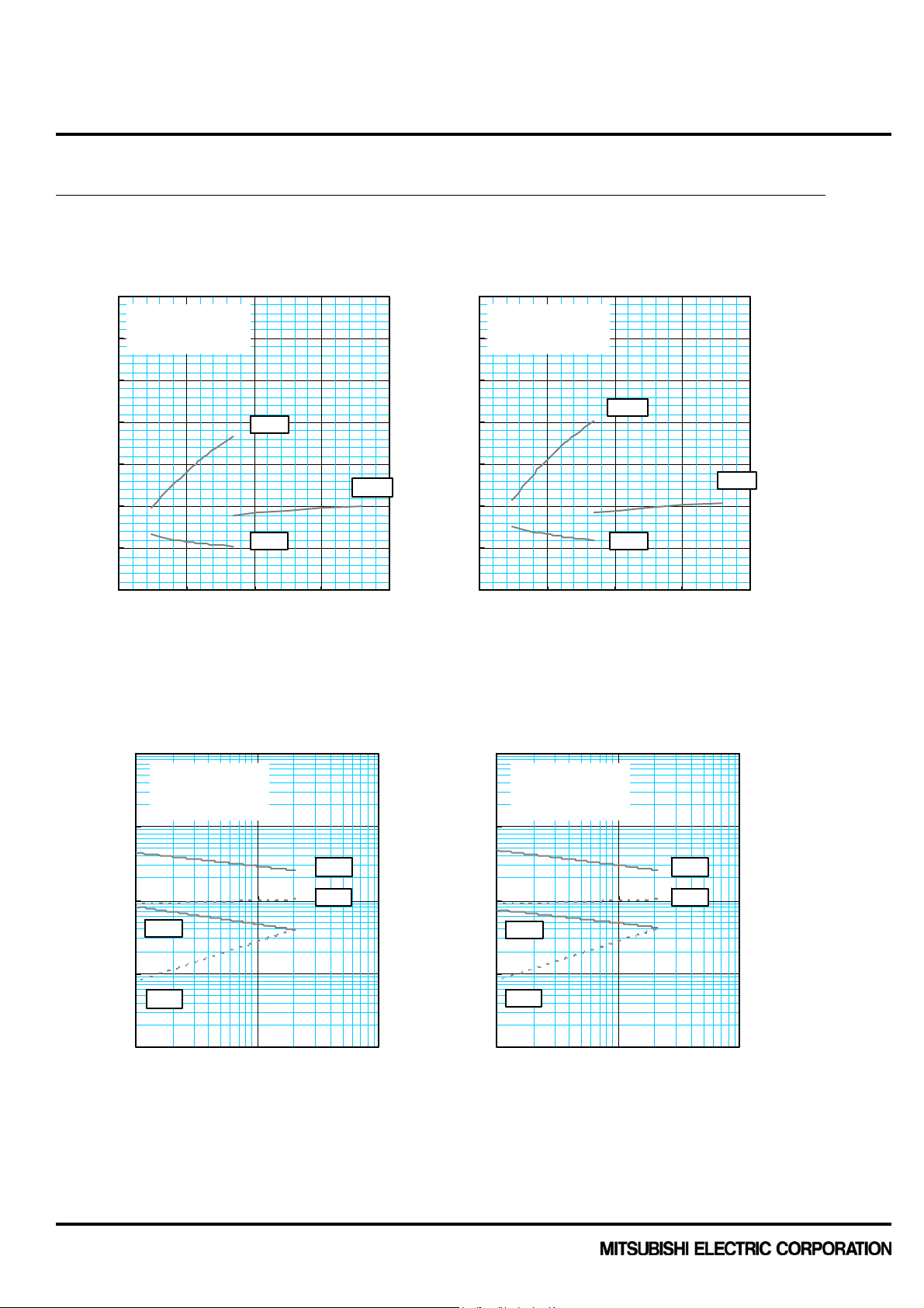
REVERSE BIAS SAFE OPERATING AREA
40 00
4th-Version HVIGBT (High Voltage Insulated Gate Bipolar Transistor) Modules
(RBSOA)
VCC 25 00 V, VGE = ± 15V
Tj = 15 0 °C , R
G(off)
= 8. 4
SHORT CIRCUIT
SAFE OPERATING AREA (SCSOA)
16
VCC 25 00V, VGE = ±1 5V
R
= 2.4, R
G(on)
Tj = 1 50° C
G( off)
= 8.4
30 00
20 00
Collector C urrent [A]
10 00
0
0 1000200030004000
Collector-Emitter Voltage [V]
FREE-WHEEL DIODE REVERSE RECOVERY
SAFE OPERATING AREA (RRSOA)
40 00
VCC 25 00 V, di /d t < 6 kA/µ s
Tj = 15 0 °C
30 00
12
8
Collector Current [kA]
4
0
0 1 000 20 00 3 000 40 00
Collector-Em itter Voltage [V]
20 00
10 00
Reverse Recovery Current [A]
0
0 1000200030004000
December 2012
Emitter-Collector Voltage [V]
(HVM-1055-F)
8

< HVIGBT MODULES >
CM1000E4C-66R
HIGH POWER SWITCHING USE
INSULATED TYPE
4th-Version HVIGBT (High Voltage Insulated Gate Bipolar Transistor) Modules
Mitsubishi Electric Corporation puts the maximum effort into making semiconductor products better and more
reliable, but there is always the possibility that trouble may occur with them. Trouble with semiconductors
may lead to personal injury, fire or property damage. Remember to give due consideration to safety when
making your circuit designs, with appropriate measures such as (i) placement of substitutive, auxiliary
circuits, (ii) use of non-flammable material or (iii) prevention against any malfunction or mishap.
•These materials are intended as a reference to assist our customers in the selection of the Mitsubishi
semiconductor product best suited to the customer’s application; they do not convey any license under any
intellectual property rights, or any other rights, belonging to Mitsubishi Electric Corporation or a third party.
•Mitsubishi Electric Corporation assumes no responsibility for any damage, or infringement of any
third-party’s rights, originating in the use of any product data, diagrams, charts, programs, algorithms, or
circuit application examples contained in these materials.
•All information contained in these materials, including product data, diagrams, charts, programs and
algorithms represents information on products at the time of publication of these materials, and are subject
to change by Mitsubishi Electric Corporation without notice due to product improvements or other reasons. It
is therefore recommended that customers contact Mitsubishi Electric Corporation or an authorized
Mitsubishi Semiconductor product distributor for the latest product information before purchasing a product
listed herein.
The information described here may contain technical inaccuracies or typographical errors. Mitsubishi
Electric Corporation assumes no responsibility for any damage, liability, or other loss rising from these
inaccuracies or errors.
Please also pay attention to information published by Mitsubishi Electric Corporation by various means,
including the Mitsubishi Semiconductor home page (http://www.MitsubishiElectric.com/).
•When using any or all of the information contained in these materials, including product data, diagrams,
charts, programs, and algorithms, please be sure to evaluate all information as a total system before making
a final decision on the applicability of the information and products. Mitsubishi Electric Corporation assumes
no responsibility for any damage, liability or other loss resulting from the information contained herein.
•Mitsubishi Electric Corporation semiconductors are not designed or manufactured for use in a device or
system that is used under circumstances in which human life is potentially at stake. Please contact
Mitsubishi Electric Corporation or an authorized Mitsubishi Semiconductor product distributor when
considering the use of a product contained herein for any specific purposes, such as apparatus or systems
for transportation, vehicular, medical, aerospace, nuclear, or undersea repeater use.
•The prior written approval of Mitsubishi Electric Corporation is necessary to reprint or reproduce in whole or
in part these materials.
•If these products or technologies are subject to the Japanese export control restrictions, they must be
exported under a license from the Japanese government and cannot be imported into a country other than
the approved destination.
Any diversion or re-export contrary to the export control laws and regulations of Japan and/or the country of
destination is prohibited.
•Please contact Mitsubishi Electric Corporation or an authorized Mitsubishi Semiconductor product distributor
for further details on these materials or the products contained therein.
Keep safety first in your circuit designs!
Notes regarding these materials
© 2011 MITSUBISHI ELECTRIC CORPORATION. ALL RIGHTS RESERVED.
December 2012
(HVM-1055-F)
9
 Loading...