

SECURITY
CODE
Spec. NAME
Customer’s
Std. Spec.
Prepared by K.Kurachi
Checked by
Approved by H.Yamaguchi
DATE 10-Apr.-2008
MITSUBISHI ELECTRIC CORPORATION
R
E
V
HIGH VOLTAGE DIODE MODULE
1. Type Number RM900DB-90S
2. Structure Flat base type (Insulated package, Cu base plate)
3. Application & Customer High power converters & Inverters for traction application
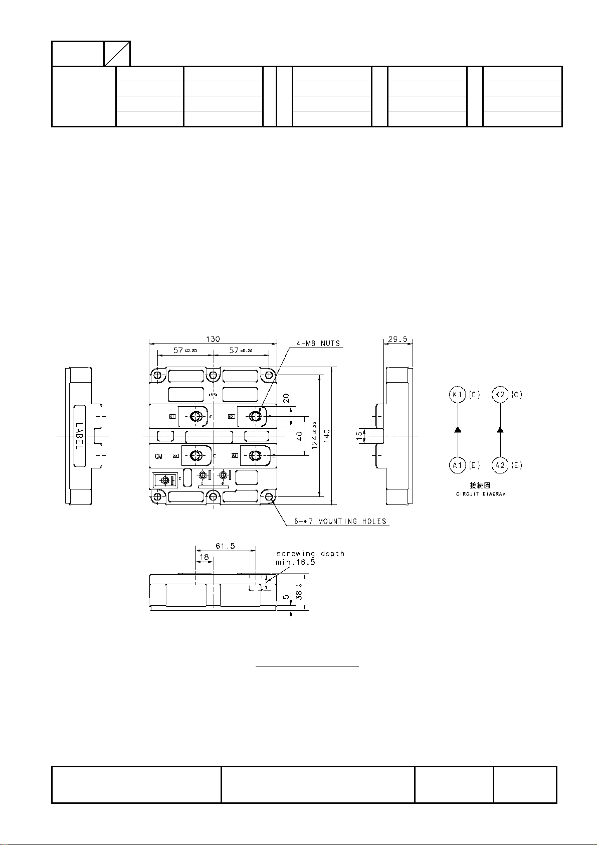
4. Outline See Fig. 1
5. Related Specifications
HIGH VOLTAGE DIODE MODULE
Fig. 1 - Outline drawing
HVM-2018
(HV-SETSU)
PAGE
1 / 11
6. Maximum Ratings
MITSUBISHI ELECTRIC CORPORATION
Item Symbol Conditions Ratings Unit
6.1 Repetitive peak reverse voltage V
6.2 Non-repetitive peak reverse
voltage
6.3 Reverse DC voltage V
6.4 DC forward current IF T
6.5 Surge forward current I
6.6 Surge current load integral I2t
6.7 Isolation voltage V
T
RRM
T
V
RSM
R(DC)
FSM
= 25 °C 4500 V
j
= 25 °C 4500 V
j
Tj = 25 °C 3000 V
= 25 °C 900 A
c
T
= 25 °C start, tw = 8.3 ms
j
Half sign wave
T
= 25 °C start, tw = 8.3 ms
j
6400 A
Half sign wave
iso
Charged part to the baseplate
RMS sinusoidal, 60Hz 1min.
6000 V
170 kA
6.8 Junction temperature Tj — −40 ~ +150 °C
6.9 Storage temperature T
— −40 ~ +125 °C
stg
6.10 Operating temperature Top — −40 ~ +125 °C
V
≤ 3000 V
6.11 Maximum reverse recovery
instantaneous power
—
R
di/dt ≤ 2600A/µs, T
[See Fig.1, Fig.2, 12-5]
= 125 °C
j
900 kW
7. Electrical Characteristics
2
s
Item Symbol Conditions
7.1 Repetitive reverse current I
RRM
7.2 Forward voltage VFM
VRM = V
IF = 900 A
RRM
(Note 1)
Tj = 25 °C
Tj = 125 °C
Tj = 25 °C
Tj = 125 °C
Limits
Min. Typ. Max.
— — 8
— 8 20
— 4.00 —
— 3.60 —
Unit
mA
V
7.3 Reverse recovery time trr — 0.9 — µs
V
= 2250 V, IF = 900 A
7.4 Reverse recovery current Irr — 900 — A
7.5 Reverse recovery charge Qrr — 650 — µC
7.6 Reverse recovery energy E
Note 1: It doesn't include the voltage drop by Internal lead resistance.
rec
R
di/dt = −1800 A/µs
= 125 °C
T
j
[See Fig.1,Fig.2]
— 0.70 — J/P
HIGH VOLTAGE DIODE MODULE
HVM-2018
(HV-SETSU)
PAGE
2 / 11
8. Thermal Characteristics
MITSUBISHI ELECTRIC CORPORATION
Item Symbol Conditions
8.1 Thermal resistance R
8.2 Contact thermal resistance R
Note 2: Thermal conductivity is 1W/mK with a thickness of 100µm.
th(j-c)R
th(c-f)
Junction to case
(per 1/2 module)
Case to fin
Conductive grease applied
(per 1/2 module)
(Note 2)
Limits
Min. Typ. Max.
Unit
— — 20.0 K/kW
— 16.0 — K/kW
9. Mechanical Characteristics
Item Symbol Conditions
9.1 Mounting torque —
9.2 Mounting torque —
Main terminal screw : M8
Mounting screw : M6
9.3 Mass — — — 1.5 — kg
9.4 Comparative tracking index CTI — 600 — — —
Limits
Min. Typ. Max.
Unit
7.0 — 13.0 N·m
3.0 — 6.0 N·m
9.5 Clearance — — 19.5 — — mm
9.6 Creepage distance — — 32 — — mm
9.7 Internal inductance L
9.8 Internal lead resistance R
— — 35 — nH
A-K(int)
A-K(int)
Tc = 25 °C — 0.25 — mΩ
10. Shipping Inspection Report Item
Static characteristics : I
Dynamic characteristics : t
Note 3: One shipping inspection report with the above item values is submitted when modules are delivered. The test
conditions are defined in bracket.
RRM
[7.3], Qrr [7.5]
rr
(note 3)
[7.1], VFM [7.2]
HIGH VOLTAGE DIODE MODULE
HVM-2018
(HV-SETSU)
PAGE
3 / 11
MITSUBISHI ELECTRIC CORPORATION
∫
∫
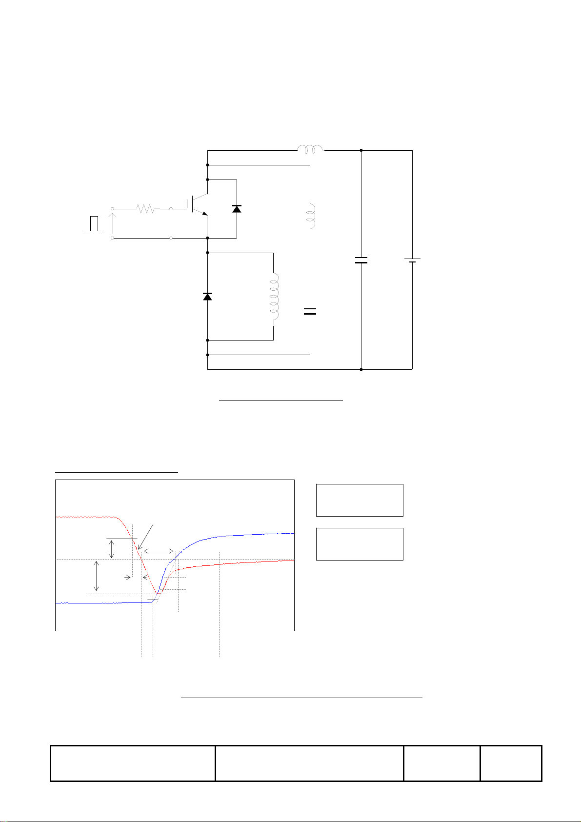
11. Test Circuit & Definition of Switching Characteristics
S1
L
Rg
L
K
LOAD
DUT: diode
L
S2
= 150 nH
C = 2 mF VCC
Diode part: reverse recovery
IF
di/dt
0
0
di
Irr
trr
dt
10%V
CS = 200 uF
A
Fig. 1 – Switching test circuit
= –
= –
t6
if dt
0
t6
if•vr dt
t5
Qrr
V
R
10%IF
50%Irr
90%Irr
R
Erec
t5
0
t6
Fig. 2 – Definitions of reverse recovery charge & energy
HIGH VOLTAGE DIODE MODULE
HVM-2018
(HV-SETSU)
PAGE
4 / 11

MITSUBISHI ELECTRIC CORPORATION
12. Performance curves
12-1 Forward characteristics...................................................................................................6
12-2 Reverse recovery energy characteristics ......................................................................7
12-3 Reverse recovery current characteristics......................................................................8
12-4 Transient thermal impedance characteristics...............................................................9
12-5 Reverse recovery safe operating area .........................................................................10
HIGH VOLTAGE DIODE MODULE
HVM-2018
(HV-SETSU)
PAGE
5 / 11

MITSUBISHI ELECTRIC CORPORATION
12-1 Forward characteristics
1800
1600
1400
1200
[A]
F
1000
Tj=125°C Tj=25°C
800
Forward current I
600
400
200
0
012345678
Forward voltage VFM [V]
Forward voltage characteristics (typical)
HIGH VOLTAGE DIODE MODULE
HVM-2018
(HV-SETSU)
PAGE
6 / 11

MITSUBISHI ELECTRIC CORPORATION
12-2 Reverse recovery energy characteristics
1.4
1.2
1.0
0.8
0.6
Reverse recovery energy Erec [J/P]
Tj = 125°C, V
= 2250V
R
Ls = 150nH, Inductive load
Integration range: 10%V
~10%IF
R
0.4
0.2
0.0
0 500 1000 1500 2000
Forward current IF [A]
Reverse recovery energy characteristics (typical)
HIGH VOLTAGE DIODE MODULE
HVM-2018
(HV-SETSU)
PAGE
7 / 11

MITSUBISHI ELECTRIC CORPORATION
A
12-3 Reverse recovery current characteristics
1400
Tj = 125°C, VR = 2250V
Ls = 150nH,
1200
1000
]
Inductive load
Reverse recovery current Irr [
800
600
400
200
0
0 500 1000 1500 2000
Forward current IF [A]
Reverse recovery current characteristics (typical)
HIGH VOLTAGE DIODE MODULE
HVM-2018
(HV-SETSU)
PAGE
8 / 11

MITSUBISHI ELECTRIC CORPORATION
12-4 Transient thermal impedance characteristics
1.2
Rth(j-c) = 20 K/kW
1.0
0.8
0.6
0.4
Normalized transient thermal impedance
0.2
0.0
0.001 0.01 0.1 1 10
Time [sec.]
Transient thermal impedance characteristics
HIGH VOLTAGE DIODE MODULE
HVM-2018
(HV-SETSU)
PAGE
9 / 11

MITSUBISHI ELECTRIC CORPORATION
12-5 Reverse recovery safe operating area
2500
2000
[A]
Tj = 125°C, VR ≤ 3000 V
di/dt ≤ 2600A/µs
1500
1000
Reverse recovery current Irr
500
0
0 1000 2000 3000 4000 5000
Reverse recovery safe operating area (RRSOA)
HIGH VOLTAGE DIODE MODULE
Reverse voltage VR [V]
HVM-2018
(HV-SETSU)
PAGE
10 / 11

MITSUBISHI ELECTRIC CORPORATION
Rev.
No.
−
Summary of changes
Original
Signature
& date
K.Kurachi
10-Apr.-2008
HIGH VOLTAGE DIODE MODULE
HVM-2018
(HV-SETSU)
PAGE
11 / 11
 Loading...