

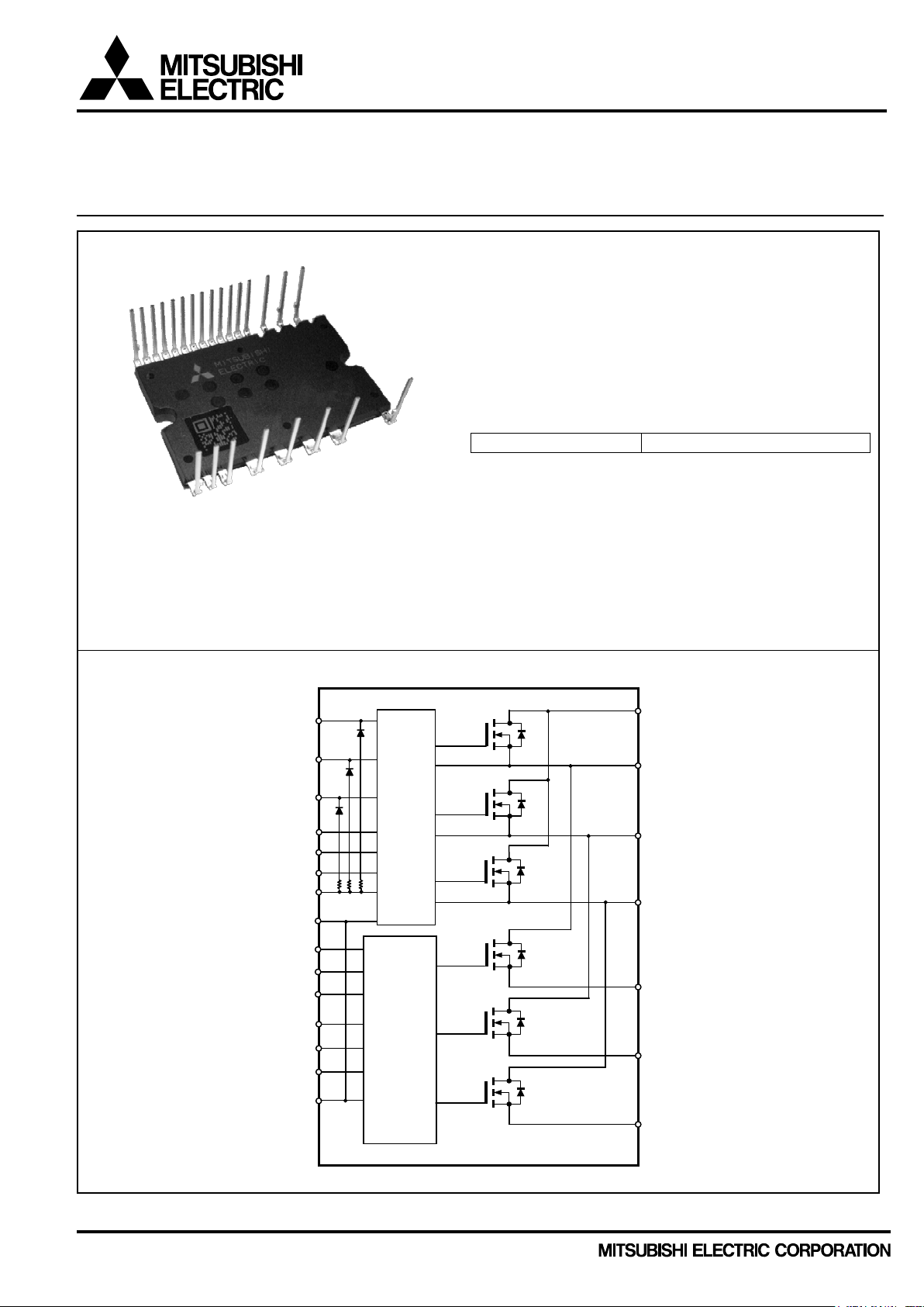
PSM05S93E5-A
With over temperature protection
V
(2)
V
(3)
V
(4)
W(21)
VP(6)
WP(7)
UP(5)
VP1(8)
VNC(9)
UN(10)
VN(11)
WN(12)
FO(14)
VN1(13)
VNC(16)
NW(18)
CIN(15)
NU(20)
NV(19)
V(22)
U(23)
P(24)
LVIC
MOSFET1
MOSFET2
MOSFET3
HVIC
MOSFET4
MOSFET5
MOSFET6
< Dual-In-Line Package Intelligent Power Module >
PSM05S93E5-A
TRANSFER MOLDING TYPE
INSULATED TYPE
OUTLINE
MAIN FUNCTION AND RATINGS
3 phase DC/AC inverter
500V / 5A (MOSFET)
N-side MOSFET open source
Built-in bootstrap diodes with current limiting resistor
APPLICATION
AC 100~240Vrms(DC voltage:400V or below) class
low power motor control
TYPE NAME
INTEGRATED DRIVE, PROTECTION AND SYSTEM CONTROL FUNCTIONS
● For P-side : Drive circuit, High voltage high-speed level shif ting , Control supply under-voltage (UV) protection
● For N-side :
Drive circuit, Control supply under-voltage prote cti on (UV) , Short circuit protection (SC),
Over temperature protection (OT)
● Fault signaling : Corresponding to SC fault (N-side MOSFET), UV fault (N-side supply) and OT fault
● Input interface : 3, 5V line, Schmitt trigger receiver circuit (High Active)
●UL Recognized : UL1557 File E323585
INTERNAL CIRCUIT
UFB
VFB
WFB
Publication Date : October 2013
1
< Dual-In-Line Package Intelligent Power Module >
INVERTER PART
Symbol Parameter Condition
Ratings
Unit
V
DD
Supply voltage
Applied between P-NU,NV,NW
400
V
±IDP
Each MOSFET drain current (peak)
TC= 25°C, less than 1ms
10
A
PD
Drain dissipation
TC= 25°C, per 1 chip
35.7
W
Tch
Channel temperature
(Note 1)
-20~+150
°C
Note1: Th e maximum junc tion tempe rature ratin g of built-in power chips is 150°C(@Tc≤100°C).However, to ensure safe operation of DIPIPM, the average
channel temperature should be limited to Tch(Ave)≤125°C (@Tc≤100°C).
CONTROL (PROTECTION) PART
Symbol Parameter Condition
Ratings
Unit
VD
Control supply voltage
Applied between
VP1-VNC, VN1-VNC
20
V
V
U
VFO
Fault output supply voltage
Applied between
FO-VNC
-0.5~VD+0.5
V
IFO
Fault output current
Sink current at FO terminal
1
mA
VSC
Current sensing input voltage
Applied between CIN-VNC
-0.5~VD+0.5
V
TOTAL SYSTEM
Symbol Parameter Condition
Ratings
Unit
Self protection supply voltage limit
(Short circuit protection capability)
VD = 13.5~16.5V, Inverter Part
Tch = 125°C, non-repetitive, less than 2μs
60Hz, Sinusoidal, AC 1min, between connected all pins
and heat sink plate
THERMAL RESISTANCE
Limits
Min.
Typ.
Max.
R
th(ch-c)Q
Junction to case thermal resistance (Note2)
1/6 module
- - 2.8
K/W
Control terminals
DIPIPM
Tc point
IGBT chip position
Heat sink side
11.6mm
Power terminals
PSM05S93E5-A
TRANSFER MOLDING TYPE
INSULATED TYPE
MAXIMUM RATINGS (T
= 25°C, unless otherwise noted)
ch
V
DD(surge)
V
DSS
±ID Each MOSFET drain current TC= 25°C 5 A
VDB Control supply voltage Applied between
VIN Input voltage Applied between
V
DD(PROT)
TC Module case operation temperature Measurement point of Tc is provided in Fig.1 -20~+100 °C
T
Storage temperature -40~+125 °C
stg
V
Isol ation vol tage
iso
Fig. 1: TC MEASUREMEN T POINT
Supply voltage (surge) Applied between P-NU,NV,NW 450 V
Drain-source voltage 500 V
-U, V
-V, V
UFB
VFB
, VP, WP-VPC, UN, VN, WN-VNC -0.5~VD+0.5 V
P
-W 20 V
WFB
400 V
1500 V
3mm
rms
Symbol Parameter Condition
Note 2: Grease with goo d thermal c onductivi ty and long -term endurance should be applied evenly with about +100μm~+200μm on the contacting surface of
DIPIPM and heat sink. The contacting therm al res istanc e bet ween D IPIP M case an d heat sink Rth( c-f) is d eterm ined by th e thick ness a nd the t herm al
conductivity of the applied grease. For reference, Rth(c-f) is about 0.3K/W (per 1/6 module, grease thickness: 20μm, thermal conductivity: 1.0W /m•k).
Publication Date : Oct ober 2013
2
Unit
< Dual-In-Line Package Intelligent Power Module >
ELECTRICAL CHARACTERISTICS
INVERTER PART
Min.
Typ.
Max.
Tch= 25°C
-
0.60
0.80
Tch= 125°C
-
1.30
1.70
VSD
Source-drain voltage drop
VIN= 0V, -ID= 5A
-
0.90
1.30
V
ton
0.65
1.15
1.65
μs
t
C(off)
- 0.10
0.20
μs
trr - 0.25 - μs
Tch= 25°C
- - 1
Tch= 125°C
- - 10
CONTROL (PROTECTION) PART
Limits
Min.
Typ.
Max.
VD=15V, VIN=0V
- - 2.80
VD=15V, VIN=5V
- - 2.80
V
SC(ref)
Short circuit trip level
VD = 15V
(Note 3)
0.43
0.48
0.53
V
UV
DBt
Trip level
7.0
10.0
12.0
V
UV
DBr
Reset level
7.0
10.0
12.0
V
UVDt
Trip level
10.3 - 12.5
V
UVDr
Reset level
10.8 - 13.0
V
V
FOH
VSC = 0V, FO terminal pulled up to 5V by 10kΩ
4.9 - - V V
FOL
VSC = 1V, IFO = 1mA
- - 0.95
V
tFO
Fault output pulse width
20 - -
μs
IIN
Input current
VIN = 5V
0.70
1.00
1.50
mA
V
th(off)
OFF threshold voltage
0.80
1.30
-
ON/OFF threshold
hysteresis voltage
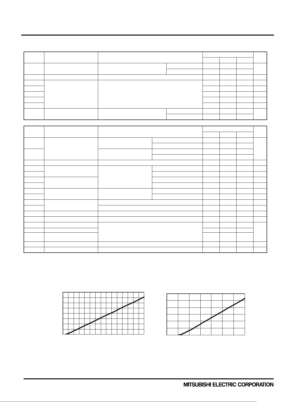
VF
Bootstrap Di forward voltage
IF=10mA including voltage drop by limiting resistor
1.1
1.7
2.3
V
Built-in limiting resistance
0
20
40
60
80
100
120
140
160
0 1 2 3 4 5 6 7
8 9 10 11 12 13
14 15
V
F
[V]
I
F
[mA]
0
5
10
15
20
25
30
0.0 0.5
1.0 1.5 2.0 2.5 3.0 3.5
VF [V]
I
F
[mA]
PSM05S93E5-A
TRANSFER MOLDING TYPE
INSULATED TYPE
(Tch = 25°C, unless otherwise noted)
Symbol Parameter Condition
V
DS(on)
t
C(on)
t
- 1.00 1.50 μs
off
Drain-source on-state
resistance
- 0.35 0.55 μs
Switching times
VD=VDB = 15V, VIN= 5V, ID= 5A
V
= 300V, VD= VDB= 15V
DD
= 5A, Tch= 125°C, VIN= 0↔5V
I
D
Limits
Unit
Ω
Inductive Load (upper-lower arm)
I
DSS
Symbol Parameter Condition
ID
IDB
Drain-source cut-off
current
Circuit current
VDS=V
DSS
Total of VP1-VNC, VN1-VNC
WFB
-W
UFB
-U,
Each part of V
V
-V, V
VFB
V
= 15V, VIN=0V - - 0.10
D=VDB
VD=VDB= 15V, VIN=5V - - 0.10
mA
Unit
mA
P-side Control supply
under-voltage protection(UV)
N-side Control supply
Tch ≤125°C
under-voltage protection(UV)
OTt
OTrh Detect LVIC temperature Hysteresis of trip-reset - 10 - °C
Over temperature protection
(OT) (Note4)
V
= 15V Trip level 100 120 140 °C
D
Fault output voltage
(Note 5)
V
ON threshold voltage
th(on)
Applied between U
V
th(hys)
R
Note 3 : SC protection works for N-side only. Please select the external shunt resistance such that the SC trip-level is less than 1.7 times of the current rating.
4 : When the LVIC temperature e xceeds OT trip tem peratu re level (OT
loosely, don't reuse that DIPIPM. (There is a possibility that channel temperature of power chips exceeded maximum Tch(150°C).
5 : Fa ult signal Fo outpu ts when SC, UV or OT protection work s. Fo pulse width is different for eac h prot ectio n modes. At SC failure, Fo pul se width is a fi xed
width (=minimum 20μs), but at UV or OT fail ur e, Fo out pu ts continuously until recovering from UV or OT state. (But minimum Fo pulse width is 20μs.)
6 : The characteristics of bootstrap Di is described in Fig.2.
Included in bootstrap Di 80 100 120 Ω
, VP, WP, UN, VN, WN-VNC
P
(Note 6)
), OT protection works and Fo outputs. In that case if the he at sink dropped off or fixed
t
- 2.10 2.60
0.35 0.65 -
Fig. 2 Characteristics of bootstrap Di VF-IF curve (@Ta=25°C) including voltage drop by limiting resistor (Right chart is enlarged chart.)
V
Publication Date : Oct ober 2013
3
< Dual-In-Line Package Intelligent Power Module >
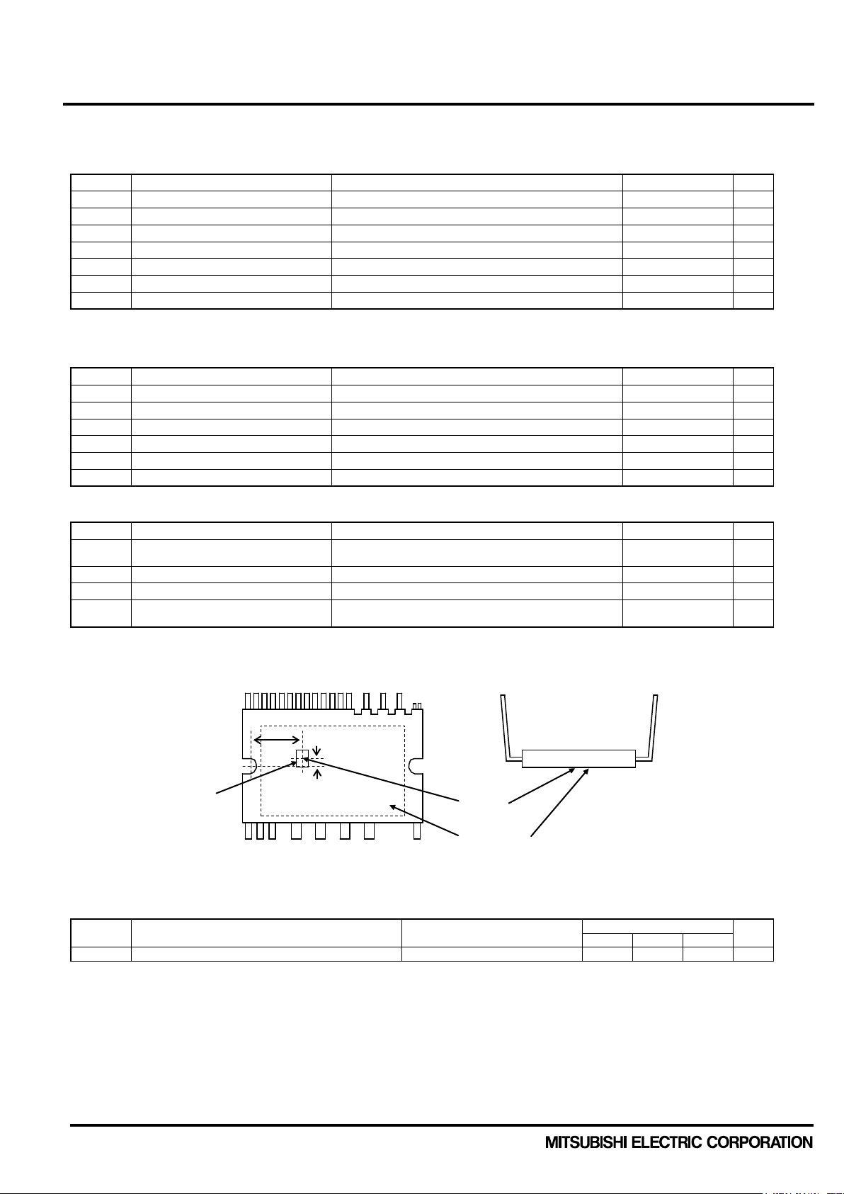
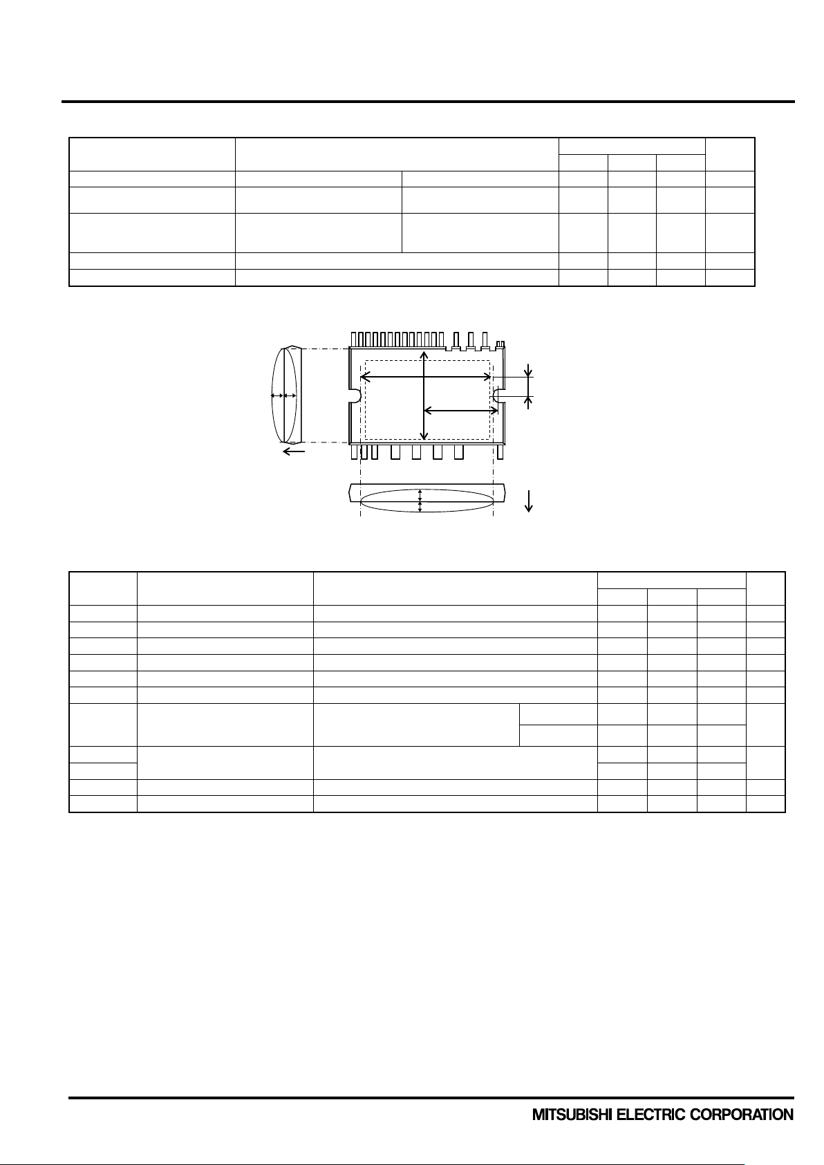
MECHANICAL CHARACTERISTICS AND RATINGS
Limits
Min.
Typ.
Max.
Control terminal: Load 4.9N
Power terminal: Load 9.8N
Control terminal: Load 2.45N
90deg. bend
Heat-sink flatness
-50 - 100
μm
RECOMMENDED OPERATION CONDITIONS
Limits
VDB
Control supply voltage
Applied between V
UFB
-U, V
VFB
-V, V
WFB
-W
13.0
15.0
18.5
V
ΔVD, ΔVDB
Control supply variation
-1 - +1
V/μs
t
dead
Arm shoot-through blocking time
For each input signal
1.0 - -
μs
f
PWM
PWM input frequency
TC ≤ 100°C, Tch ≤ 125°C
- - 20
kHz
VNC
VNC variation
Between VNC-NU, NV, NW (including surge)
-5.0 - +5.0
Tch
Channel temperature
-20 - +125
°C
4.6mm
-
+
Heat sink side
Heat sink side
Measurement position
17.5mm
+
-
PSM05S93E5-A
TRANSFER MOLDING TYPE
INSULATED TYPE
Parameter Condition
Mounting torque Mounting screw : M3 (Note 8) Recommended 0.69N·m 0.59 0.69 0.78 N·m
Terminal pulling strength
Terminal bending strength
Power terminal: Load 4.9N
EIAJ-ED-4701 10 - - s
EIAJ-ED-4701 2 - - times
Weight - 8.5 - g
(Note 9)
Note 8: Plain washers (ISO 7089~7094) are recommended.
Note 9: Measurement point of heat sink flatness
Unit
Symbol Parameter Condition
Min. Typ. Max.
VCC Supply voltage Applied between P-NU, NV, NW 0 300 400 V
VD Control supply voltage Applied between VP1-VNC, VN1-VNC 13.5 15.0 16.5 V
= 300V, VD = 15V, P.F = 0.8,
V
DD
IO Allowable r.m.s. current
PWIN(on)
PWIN(off) 0.7 - -
Note 10: Allowable r.m.s. current depends on the actual application conditions.
11: DIPIPM might not make response if the input signal pulse width is less than PWIN(on), PWIN(off).
Minimum input pulse width
Sinusoidal PWM
T
≤ 100°C, Tch ≤ 125°C (Note10)
C
= 5kHz - - 2.5
f
PWM
f
= 15kHz - - 2.0
PWM
(Note 11)
0.7 - -
Unit
Arms
μs
V
Publication Date : Oct ober 2013
4
< Dual-In-Line Package Intelligent Power Module >
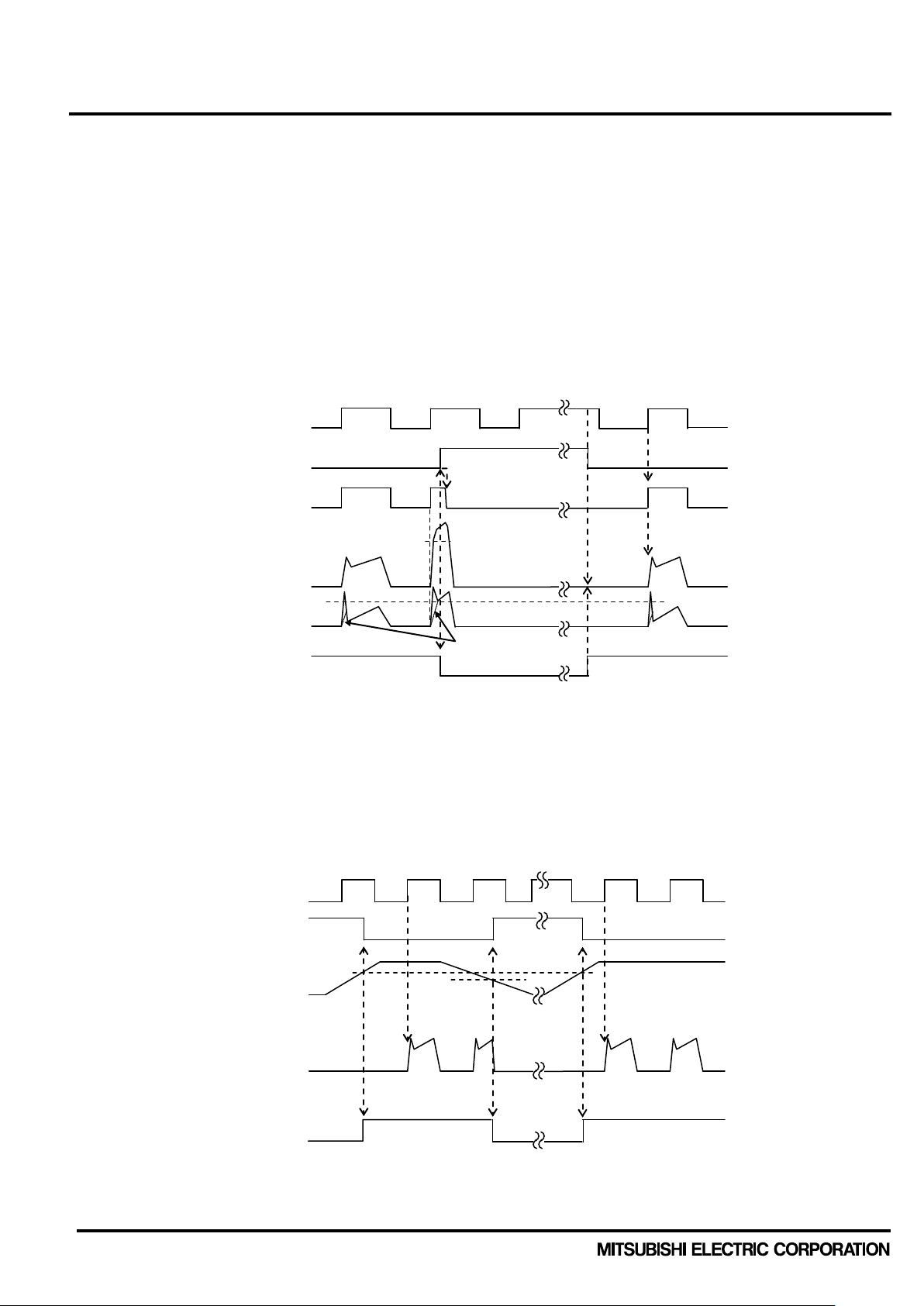
Lower-side control
input
Protection circuit state
Internal gate
Output current ID
Sense voltage of
the
Error output Fo
SC trip current level
a2
SET
RESET
SC reference voltage
a1
a3
a6
a7
a4
a8
a5
Delay by RC filtering
RESET
SET
RESET
UVDt
b1
b2
b3
b4
b6
b7
b5
Control input
Protection circuit state
Control supply voltage VD
Output current ID
Error output Fo
PSM05S93E5-A
TRANSFER MOLDING TYPE
INSULATED TYPE
Fig. 3 Timing Charts of The DIPIPM Protective Functions
[A] Short-Circuit Protection (N-side only with the external shunt resistor and RC filter)
a1. Normal operation: MOSFET ON and outputs current.
a2. Short circuit current detection (SC trigger)
(It is recommended to set RC time constant 1.5~2.0μs so that MOSFET shut down within 2.0μs when SC.)
a3. All N-side MOSFET's gates are hard interrupted.
a4. All N-side MOSFETs turn OFF.
a5. F
outputs for tFo=minimum 20μs.
O
a6. Input = “L”: MOSFET OFF
a7. Fo finishes output, but MOSFETs don't turn on until inputting next ON signal (LH).
(MOSFET of each phase can return to normal state by inputting ON signal to each phase.)
a8. Normal operation: MOSFET ON and outputs current.
shunt resistor
[B] Under-Voltage Protection (N-side, UV
b1. Control supply voltage V
(MOSFET of each phase can return to normal state by inputting ON signal to each phase.)
b2. Normal operation: MOSFET ON and outputs current.
b3. V
level drops to under voltage trip level. (UVDt).
D
b4. All N-side MOSFETs turn OFF in spite of control input condition.
b5. Fo outputs for t
b6. V
level reaches UVDr.
D
b7. Normal operation: MOSFET ON and outputs current.
=minimum 20μs, but output is extended during VD keeps below UVDr.
Fo
exceeds under voltage reset level (UVDr), but MOSFET turns ON by next ON signal (LH).
D
)
D
UVDr
Publication Date : Oct ober 2013
5
< Dual-In-Line Package Intelligent Power Module >
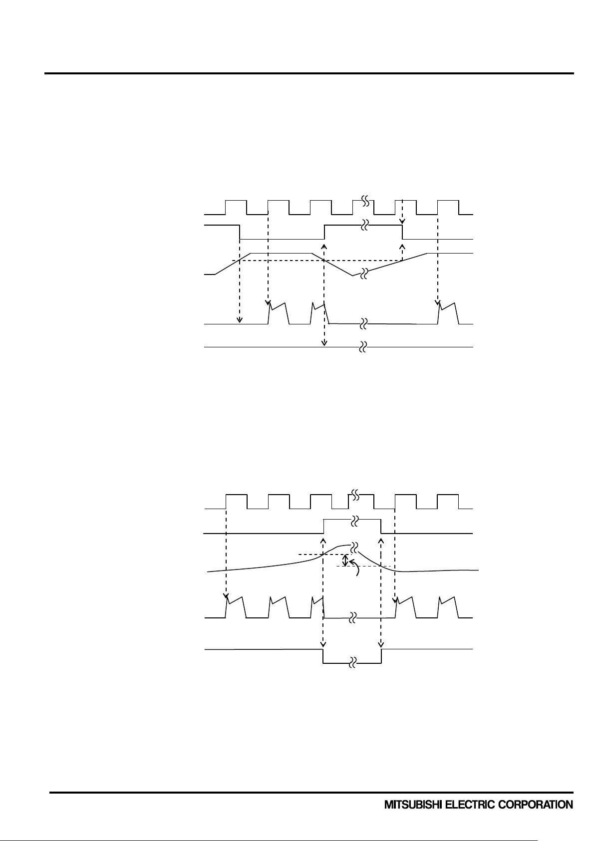
Control input
Protection circuit state
Control supply voltage VDB
Output current ID
Error output Fo
UV
RESET
SET
RESET
UV
Keep High-level (no fault output)
c1
c2
c3
c4
c5
c6
SET
RESET
OTt
d1
d2
d3
d5
d6
d4
OTt - OT
Control input
Protection circuit state
Temperature of LVIC
Output current ID
Error output Fo
PSM05S93E5-A
TRANSFER MOLDING TYPE
INSULATED TYPE
[C] Under-Voltage Protection (P-side, UVDB)
c1. Control supply voltage VDB rises. After the voltage reaches under voltage reset level UV
c2. Normal operation: MOSFET ON and outputs current.
c3. V
level drops to under voltage trip level (UV
DB
DBt
).
c4. MOSFET of the correspond phase only turns OFF in spite of control input signal level, but there is no F
c5. V
level reaches UV
DB
DBr
.
c6. Normal operation: MOSFET ON and outputs current.
DBr
DBt
[D] Over Temperature Protection (N-side, Detecting LVIC temperature)
d1. Normal operation: MOSFET ON and outputs current.
d2. LVIC temperature exceeds over temperature trip level(OT
d3. All N-side MOSFETs turn OFF in spite of control input condition.
d4. Fo outputs for t
=minimum 20μs, but output is extended during LVIC temperature keeps over OTt.
Fo
d5. LVIC temperature drops to over temperature reset level.
d6. Normal operation: MOSFET turns on by next ON signal (LH).
(MOSFET of each phase can return to normal state by inputting ON signal to each phase.)
).
t
, MOSFET turns on by next ON signal (LH).
DBr
rh
signal output.
O
Publication Date : Oct ober 2013
6
< Dual-In-Line Package Intelligent Power Module >
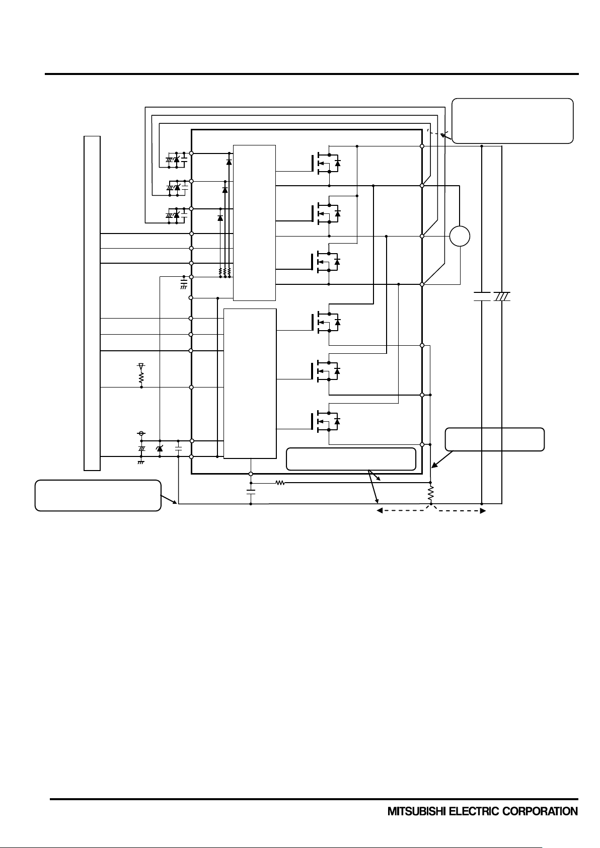
Long GND wiring might generate
Long wiring might cause SC level
fluctuation and malfunction.
Long wiring might cause
short circuit failure
Bootstrap negative electrodes
terminals directly and separated
Power GND wiring
Control GND wiring
D1 + +
MCU
C2
15V VD
M
C4
R1
Shunt
resistor
N1 B C
5V A C2
V
(2)
V
(3)
V
(4)
+
UN(10)
VN(11)
WN(12)
Fo(14)
VN1(13)
VNC(16)
P(24)
U(23)
W(21)
LVIC
V(22)
VP(6)
WP(7)
UP(5)
VP1(8)
CIN(15)
MOSFET1
MOSFET2
MOSFET3
C1
C1
C2 + D
D1
VNC(9)
C3
HVIC
NW(18)
MOSFET4
MOSFET5
MOSFET6
NU(20)
NV(19)
+
PSM05S93E5-A
TRANSFER MOLDING TYPE
INSULATED TYPE
Fig. 4 Example of Applicatio n Circuit
UFB
VFB
WFB
noise to input signal and cause
(1) If control GND is connected with power GND by c om m on broad pattern, it may cause malfunction by power G N D fluctuation.
It is recommended to connect control GND and power GN D at only a point N1 (near the terminal of shunt resistor).
(2) It is recommended t o insert a Zener diode D1(24V/1W) between each pair of control supply terminals to prevent surge destruction.
(3) To prevent surge destr uction, the wiring between the smoothing capacitor and the P, N1 terminals should be as short as possible.
Generally a 0.1-0.22μF snubber capacitor C3 between the P-N1 terminals is recommended.
(4) R1, C4 of RC filter for preventi ng protection c ircuit malf unction is r ecommended to selec t tight toler ance, temp-com pensated type.
The time constant R1C4 should be set so that SC current is shut down within 2μs. (1.5μs~2μs is general value.) SC interrupting time
might vary with the wiring pattern, so the enoug h evaluation on the real system is necessar y.
(5) To prevent malfunction, the wiring of A, B, C should be as short as possible.
(6) The point D at which t he wi ri ng to CI N fi l ter i s divi ded shoul d be near t he terminal of shunt res i stor. NU, NV, NW terminals should be
connected at near N U, NV, NW terminals.
(7) All capacitors s hould be mounte d as cl ose to the ter minals as possible. (C1: good t emperature, frequenc y characteristic electrolytic
type and C2:0.22μ-2μF, good temperature, frequency and DC bias characteristic ceramic t ype are recommended.)
(8) Input drive is Hi gh-active type. There is a minimum 3.3kΩ pull-down resistor in the input circuit of IC. To prevent malfunction, the
wiring of each input should be as short as possible. When using RC coupling circuit, make sure the input signal level meet the turn-on
and turn-off threshold voltage.
(9) Fo output is open drain type. It should be pul led up to MCU or control power supply ( e.g. 5V,15V) by a resistor that makes I
1mA. (I
is estimated roughly by the formula of control power supply voltage divided by pull-up resistance. In the case of pulled up to
FO
5V, 10kΩ (5kΩ or more) is recommended.)
(10) Thanks to built-in HVIC, direct coupling to MC U w ithout any opto-coupl er or transformer isolation is possible.
(11) Two V
termi nals (9 & 16 pin) are connected i nside DIP IPM, please c onnect eit her one to the 15V pow er supply G ND outside and
NC
leave another one open.
(12) If high frequency noise superimposed to the control supply line, IC malfunction might happen and cause DIPIPM erroneous operation.
To avoid such problem, l ine ripple voltage should meet dV /dt ≤+/-1V/μs, Vripple≤2Vp-p.
(13) For DIPIPM, it isn't recommended to drive same load by parallel connection w ith other phase MOSFET or other DIPIPM.
should be connected to U,V,W
from the main output wires
Fo
up to
Publication Date : Oct ober 2013
7

UP,VP,WP,UN,VN,WN
Fo
VNC(Logic)
DIPIPM
MCU
10kΩ
5V line
3.3kΩ(min)
Note)
Wiring Inductance should be less than 10nH.
Inductance of a copper pattern with
NU, NV, NW should be connected
N1
VNC
NU
NW
DIPIPM
VNC
GND wiring fr o m VNC should
connected close to the
terminal of shunt resistor.
Shunt
resistor
DIPIPM
NU
N1
GND wiring fro m VNC should
connected close to the
terminal of shunt resistor.
Shunt
Each wiring Inductance should be less than 10nH.
Inductance of a copper pattern with
length=17mm, width=3mm is about 10nH.
Comparators
(Open collector output type)
External protection circuit
OR output
-
Vref
+
Vref
Vref
Shunt
resistors
5V
B A C
D
N1
-
+
- + V U W
DIPIPM
P
N-side MOSFETs
P-side MOSFETs
Drive circuit
V
NC
NW
Drive circuit
CIN
NV
NU
Protection circuit
< Dual-In-Line Package Intelligent Power Module >
PSM05S93E5-A
TRANSFER MOLDING TYPE
INSULATED TYPE
Fig. 5 MCU I/O Interface Circuit
Fig. 6 Pattern Wiring Around the Shunt Resistor
each other at near terminals.
length=17mm, width=3mm is about 10nH.
NV
NW
be
Low inductance shunt resistor like surface mounted (SMD) type is recommended.
Fig. 7 Pattern Wiring Around the Shunt Resistor (for the case of open source)
When DIPIPM is operated with three shunt resistors, voltage of each shunt resistor cannot be input to CIN terminal directly. In that case, it is necessary to use
the external protection circuit as below.
(1) It is necessary to set the time constant R
SC interrupting time might vary with the wiring pattern, comparator speed and so on.
(2) It is recommended for the threshold voltage Vref to set to the same rating of short circuit trip level (Vsc(ref): typ. 0.48V).
(3) Select the exter nal shu nt res is tance so that SC trip-level is less than specifie d value (=1.7 times of rating current).
(4) To avoid malfunction, the wiring A, B, C should be as short as possible.
(5) The point D at which the wiring to comparator is divided should be close to the terminal of shunt resistor.
(6) OR output high level when pr ote c tio n w ork s should be over 0.53V (=maximum Vsc(ref) rating).
of external comparator input so that MOSFET stops within 2μs when short circuit occurs.
fCf
Design for input RC filter depe nds on PW M control s cheme used
in the application and wiring impedance of the printed circuit board.
DIPIPM input signal interface integrates a minimum 3.3kΩ
pull-down resistor. Therefore, when inserting RC filter, it is
necessary to satisfy turn-on threshold voltage requirement.
Fo output is open d rain type. It should be pulled up to control
power supply (e.g. 5V, 15V) with a resistor that makes Fo sink
current I
(5kΩ or more) is recommended.
Rf
C
f
1mA or less. In the case of pulled up to 5V supply, 10kΩ
Fo
NV
resistors
be
Publication Date : Oct ober 2013
8

< Dual-In-Line Package Intelligent Power Module >
1-A
NC(VNC)
1-B
NC(VP1)
2
V
UFB
3 V
VFB
4 V
WFB
5 UP 6 VP 7 WP 8 VP1 9 VNC *1
10
UN
11
VN
12
WN
13
VN1
14
Fo
15
CIN
16
VNC *1
17
NC
18
NW
19
NV
20
NU
21 W 22 V 23 U 24 P 25
NC
PSM05S93E5-A
TRANSFER MOLDING TYPE
INSULATED TYPE
Fig. 8 Package Outlines
Long terminal type (PSM05S93E5-A)
Dimensions in mm
TERMINAL CODE
1) 9 & 16 pins (VNC) are connected inside DIPIPM, please connect either one to the control power supply GND outside and leave another one open.
QR Code is registered trademark of DENSO WAVE INCORPORATED in JAPAN and other countries.
Publication Date : Oct ober 2013
9

< Dual-In-Line Package Intelligent Power Module >
1
10/15/2013
-
New
PSM05S93E5-A
TRANSFER MOLDING TYPE
INSULATED TYPE
Revision Record
Rev. Date Page Revised contents
Publication Date : Oct ober 2013
10

< Dual-In-Line Package Intelligent Power Module >
Keep safety first in your cir c uit des igns!
reliable, but there is always the possibility that trouble may occur with them. Trouble with semiconductors
may lead to personal injury, fire or property damage. Remember to give due consideration to safety when
circuit designs, with appropriate measures such as (i) placement of substitutive, auxiliary
Notes regarding these ma t er ials
These materials are intended as a reference to assist our customers in the selection of the Mitsubishi
Mitsubishi Electric Corporation assumes no responsibility for any damage, or infringement of any
All information contained in these materials, including product data, diagrams, charts, programs and
Mitsubishi Electric Corpor ation witho ut notice d ue to product impr ovement s or other reasons. I t
ic Corporation or an authorized
Electric Corporation assumes no responsibility for any damage, liability, or other loss rising from these
Please also pay attention to information published by Mitsubishi Electric Corporation by various means,
When using any or all of the information contained in these materials, including product data, diagrams,
on the applicability of the information and products. Mitsubishi El ect r ic Corporation assumes
lectric Corporation semiconductors are not designed or manufactured for use in a device or
system that is used under circumstances in which human life is potentially at stake. Please contact
Corporation or an authorized Mitsubishi Semiconductor product distributor when
product contained herein for any specific purposes, such as apparatus or systems
export contrary to the export control laws and regulations of Japan and/or the country of
Please contact Mit su bish i Electr ic Corpor at ion or a n authoriz ed Mitsubishi Semiconduct or produ ct distr ibutor
PSM05S93E5-A
TRANSFER MOLDING TYPE
INSULATED TYPE
Mitsubishi Electric Cor por ation put s the m ax imum effort into making semicond uctor product s bet ter and mo r e
making your
circuits, (ii) use of non-flammable material or (iii) pr evention against any malfunction or mishap.
•
semiconductor product best suited to the customer’s application; they do not convey any license under any
intellectual property rights, or any other rights, belonging to Mitsub is hi E lectric Corporation or a third party.
•
third-party’s rights, originating in the use of any product data, diagrams, charts, programs, algorithms, or
circuit application exam pl es contained in these mat er ia ls.
•
algorithms represents information on products at the time of publication of these materials, and are subject
to change by
is therefore recommended that customers contact Mitsubishi Electr
Mitsubishi Semiconductor product distributor for the latest product information before purchasing a product
listed herein.
The information described here may contain technical inaccuracies or typographical errors. Mitsubishi
inaccuracies or errors.
including the Mitsubi s hi Semiconductor home page (http://www.MitsubishiElectric.com/).
•
charts, programs, and alg orithms, ple ase be sure to ev aluate all informat ion as a tot al system before making
a final decision
no responsibility for any dam age, l iability or other loss resulting from the information contained herein.
•Mitsubishi E
Mitsubishi Electric
considering the use of a
for transportation, vehicular, medical, aerospace, nuclear , or under sea repeater use.
•The prior written approval of Mitsubishi Electric Corporation is necessary to reprint or reproduce in whole or
in part these materials.
•If these products or technologies are subject to the Japanese export control restrictions, they must be
exported under a license from the Japanese government and cannot be imported into a country other than
the approved destination.
Any diversion or redestination is prohibited.
Publication Date : Oct ober 2013
•
for further details on these materials or the products contained therein.
© 2013 MITSUBISHI ELECTRIC CORPORAT ION. ALL RIGHTS RESERVED.
DIPIPM and CSTBT are registered trademarks of MITSUBISHI ELECTRIC CORPORATION.
11
 Loading...