

Mitsubishi TM15T3B-M, TM15T3B-H Datasheet
Feb.1999
MITSUBISHI THYRISTOR MODULES
TM15T3A-M,-H
MEDIUM POWER GENERAL USE
INSULATED TYPE
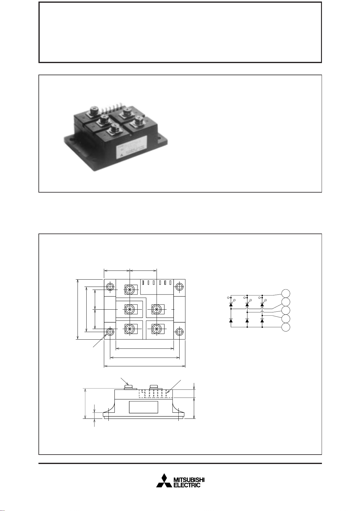
OUTLINE DRAWING & CIRCUIT DIAGRAM Dimensions in mm
APPLICATION
DC motor control, NC equipment, AC motor control, contactless switches,
electric furnace temperature control, light dimmers
TM15T3A-M,-H
• IO DC output current ...................... 30A
• V
RRM Repetitive peak reverse voltage
........ 400/800V
• V
DRM Repetitive peak off-state voltage
........ 400/800V
• 3 Phase Mix Bridge
• Insulated Type
• UL Recognized
Yellow Card No. E80276 (N)
File No. E80271
P
R
S
T
N
31 27
62
45
20 20
4–φ5.5
61.7
74
86
P
N
R
S
T
KT
GT
KS
GS
KR
GR
Tab#110, t=0.5
5–M5
31
6
722
KR KS KT
GR GS
GT
LABEL

Feb.1999
Unit
A
A
A
2
s
A/µs
W
W
V
V
A
°C
°C
V
N·m
kg·cm
N·m
kg·cm
g
ABSOLUTE MAXIMUM RATINGS
Unit
V
V
V
V
V
V
MITSUBISHI THYRISTOR MODULES
TM15T3A-M,-H
MEDIUM POWER GENERAL USE
INSULATED TYPE
M
400
480
320
400
480
320
H
800
960
640
800
960
640
Symbol
V
RRM
VRSM
VR (DC)
VDRM
VDSM
VD (DC)
Parameter
Repetitive peak reverse voltage
Non-repetitive peak reverse voltage
DC reverse voltage
Repetitive peak off-state voltage
Non-repetitive peak off-state voltage
DC off-state voltage
Conditions
3-phase fullwave rectified, TC=104°C
One half cycle at 60Hz, peak value
Value for one cycle of surge current
V
D=1/2VDRM, IG=0.5A, Tj=125°C
Charged part to case
Main terminal screw M5
Mounting screw M5
Typical value
Ratings
30
300
3.8 × 10
2
100
5.0
0.5
10
5.0
2.0
–40~125
–40~125
2500
1.47~1.96
15~20
1.47~1..96
15~20
310
Symbol
I
O
ITSM, IFSM
I
2
t
di/dt
P
GM
PG (AV)
VFGM
VRGM
IFGM
Tj
Tstg
Viso
—
—
Parameter
DC output current
Surge (non-repetitive) current
I
2
t
for fusing
Critical rate of rise of on-state current
Peak gate power dissipation
Average gate power dissipation
Peak gate forward voltage
Peak gate reverse voltage
Peak gate forward current
Junction temperature
Storage temperature
Isolation voltage
Mounting torque
Weight
Voltage class
ELECTRICAL CHARACTERISTICS
Unit
mA
mA
V
V/µs
V
V
mA
°C/W
°C/W
MΩ
Limits
Symbol
I
RRM
IDRM
VTM, VFM
dv/dt
V
GT
VGD
IGT
Rth (j-c)
Rth (c-f)
—
Parameter
Repetitive peak reverse current
Repetitive peak of off-state
current
Forward voltage
Critical rate of rise of off-state voltage
Gate trigger voltage
Gate non-trigger voltage
Gate trigger current
Thermal resistance
Contact thermal resistance
Insulation resistance
Test conditions
T
j=125°C, VRRM applied
T
j=125°C, VDRM applied
T
j=125°C, ITM=IFM=75A, instantaneous meas.
T
j=125°C, VD=2/3VDRM
Tj=25°C, VD=6V, RL=2Ω
T
j=125°C, VD=1/2VDRM
Tj=25°C, VD=6V, RL=2Ω
Junction to case (per 1/6 module)
Case to fin, Conductive grease applied (per 1/6 module)
Measured with a 500V megohmmeter between main terminal
and case
Min.
—
—
—
500
—
0.25
10
—
—
10
Typ.
—
—
—
—
—
—
—
—
—
—
Max.
4.0
4.0
1.5
—
2.0
—
50
1.8
0.36
—
Note: Items of the above table applies to the Thyristor part and the Diode part as circled in the following tables.
 Loading...