

Page 1
Silicon RF Power Semiconductors
ELECTROSTATIC SENSITIVE DEVICE
OBSERVE HANDLING PRECAUTIONS
RA01L8693MA
RoHS Compliance , 865-928MHz 1.4W 3.3V, 2 Stage Amp. For RFID READER / WRITER
DESCRIPTION
The RA01L8693MA is a 1.4-watt RF MOSFET Amplifier Module.
The battery can be connected directly to the drain of the
enhancement-mode MOSFET transistors.
The output power and drain current increase as the gate voltage
increases. With a gate voltage around 0.5V (minimum), output
power and drain current increases substantially. The nominal
output power becomes available at 1.5V (typical) and 2.0V
(maximum). At VGG=2.0V, the typical gate current is 1mA.
FEATURES
• Enhancement-Mode MOSFET Transistors
(IDD0 @ VDD=3.3V, VGG=0V)
• P
>1.4W, ηT>38% @ VDD=3.3V, VGG=2.0V, Pin=30mW
out
• Broadband Frequency Range: 865-928MHz
• Low-Power Control Current IGG=1mA (typ) at VGG=2.0V
• Module Size: 9.1 x 9.2 x 1.8 mm
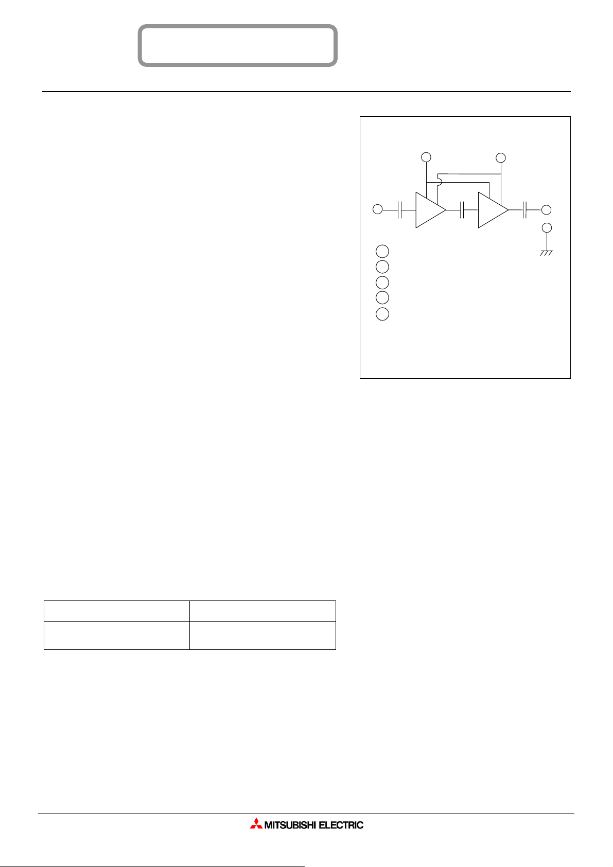
BLOCK DIAGRAM
2
1
1 RF Input (Pin)
2 Gate Voltage (VGG), Power Control
3 Drain Voltage (VDD), Battery
4 RF Output (P
5 RF Ground
out
)
3
PACKAGE CODE: H58
4
5
RoHS COMPLIANCE
• RA01L8693MA -101 is a RoHS compliance products.
• RoHS compliance is indicate by the letter “G” after the Lot Marking.
• This product include the lead in the Glass of electronic parts and the
lead in electronic Ceramic parts.
How ever,it is applicable to the following exceptions of RoHS Directions.
1.Lead in the Glass of a cathode-ray tube, electronic parts, and
fluorescent tubes.
2.Lead in electronic Ceramic parts.
ORDERING INFORMATION:
ORDER NUMBER SUPPLY FORM
RA01L8693MA -101
Antistatic tray,
168 modules/tray
RA01L8693MA 22 Jun 2010
1/12
Page 2
ELECTROSTATIC SENSITIVE DEVICE
OBSERVE HANDLING PRECAUTIONS
RoHS COMPLIANT
Silicon RF Power Semiconductors
RA01L8693MA
MAXIMUM RATINGS
(T
=+25deg.C. unless otherwise specified)
case
SYMBOL PARAMETER CONDITIONS RATING UNIT
V
V
P
P
T
case(OP)
T
Drain Voltage VGG<2.0V, ZG=ZL=50ohm 6 V
DD
Gate Voltage VDD<3.3V, Pin=0mW, ZG=ZL=50ohm 3 V
GG
Input Power 50 mW
in
Output Power 4 W
out
Operation Case Temperature Range
Storage Temperature Range -40 to +110
stg
f=865-928MHz, VGG<2.0V
ZG=ZL=50ohm
-30 to +90
°C
°C
The above parameters are independently guaranteed.
ELECTRICAL CHARACTERISTICS
(T
=+25°C, ZG=ZL=50, unless otherwise specified)
case
SYMBOL PARAMETER CONDITIONS MIN TYP MAX UNIT
f Frequency Range 865 - 928 MHz
P
η
2f
— Stability
— Load VSWR Tolerance
Output Power 1.4 - - W
out
Total Efficiency 38 - - %
T
2ndHarmonic - - -30 dBc
o
Input VSWR
in
VDD=3.3V
VGG=2.0V
PiN=30mW
- - 4.4:1 —
VDD=2.5/3.3/6.0V, VGG=0.5-2.0V,
PIN=20-50mW , Po<2.5W
No parasitic oscillation —
Zg=50ohm, Load VSWR=4:1
VDD=6.0V, PiN=30mW,
P
=2W (VGGcontrol),
out
No degradation or destroy —
Zg=50ohm, Load VSWR=20:1
All parameters, conditions, ratings, and limits are subject to change without notice.
RA01L8693MA 22 Jun 2010
2/12
Page 3
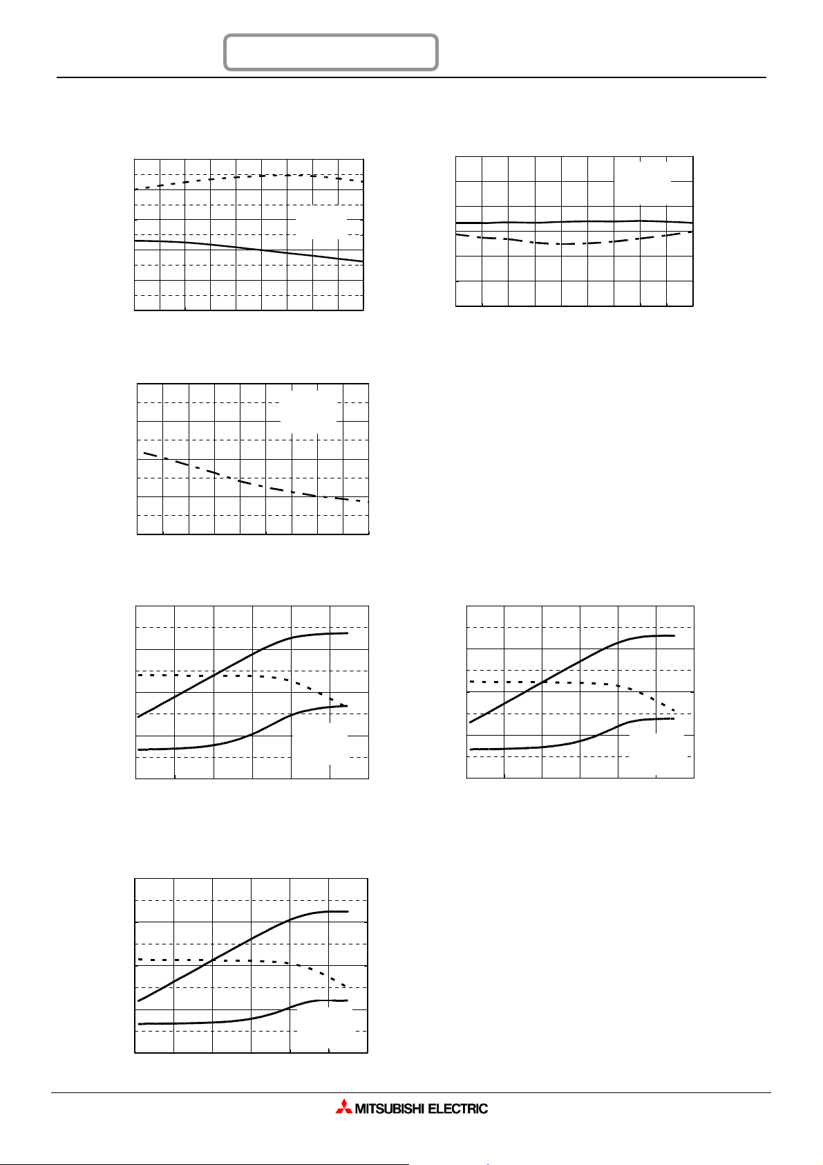
ELECTROSTATIC SENSITIVE DEVICE
versus FREQUENCY
INPUT VSWR versus FREQUENCY
in
OUTPUT POWER, POWER GAIN and
OUTPUT POWER, POWER GAIN and
DRAIN CURRENT versus INPUT POWER
DRAIN CURRENT versus INPUT POWER
OUTPUT POWER, POWER GAIN and
DRAIN CURRENT versus INPUT POWER
OBSERVE HANDLING PRECAUTIONS
RoHS COMPLIANT
Silicon RF Power Semiconductors
RA01L8693MA
TYPICAL PERFORMANCE (Vdd=3.3V,T
OUTPUT POWER, TOTAL EFFICIENCY, 2nd, 3rdHARMONICS versus FREQUENCY
5
4
(W)
out
3
2
OUTPUT POWERP
1
0
(-)
in
r
INPUTVSWR
P
out
850 860 870 880 890 900 910 920 930 940
5
4
3
2
FREQUENCY f(MHz)
VDD=3.3V
VGG=2.0V
Pin=30mW
r
=+25deg.C, ZG=ZL=50, unless otherwise specified)
case
-30
-35
-40
-45
-50
HARMONICS(dBc)
-55
-60
850 860 870 880 890 900 910 920 930 940
2nd
FREQUENCY f(MHz)
VDD=3.3V
VGG=2.0V
50
45
40
35
30
25
20
15
TOTALEFFICIENCY(%)
10
5
0
VDD=3.3V
VGG=2.0V
Pin=30mW
3rd
1
850 860 870 880 890 900 910 920 930 940
FREQUENCY f(MHz)
40
30
(dBm)
out
Gp
20
10
POWER GAIN Gp(dB)
OUTPUT POWER P
IDD
f=865MHz,
VDD=3.3V,
VGG=2.0V
0
-10 -5 0 5 10 15 20
INPUT POWER Pin(dBm)
40
30
(dBm)
out
Gp
4
P
out
(A)
3
DD
2
1
DRAIN CURRENT I
0
40
P
out
30
(dBm)
out
Gp
20
10
POWER GAIN Gp(dB)
OUTPUT POWER P
IDD
f=900MHz,
VDD=3.3V,
VGG=2.0V
0
4
(A)
3
DD
I
2
1
DRAIN CURRENT
0
-10 -5 0 5 10 15 20
INPUT POWER Pin(dBm)
4
P
out
(A)
3
DD
20
10
POWER GAIN Gp(dB)
OUTPUT POWER P
0
-10 -5 0 5 10 15 20
INPUT POWER Pin(dBm)
RA01L8693MA 22 Jun 2010
IDD
f=928MHz,
VDD=3.3V,
VGG=2.0V
2
1
DRAIN CURRENT I
0
3/12
Page 4
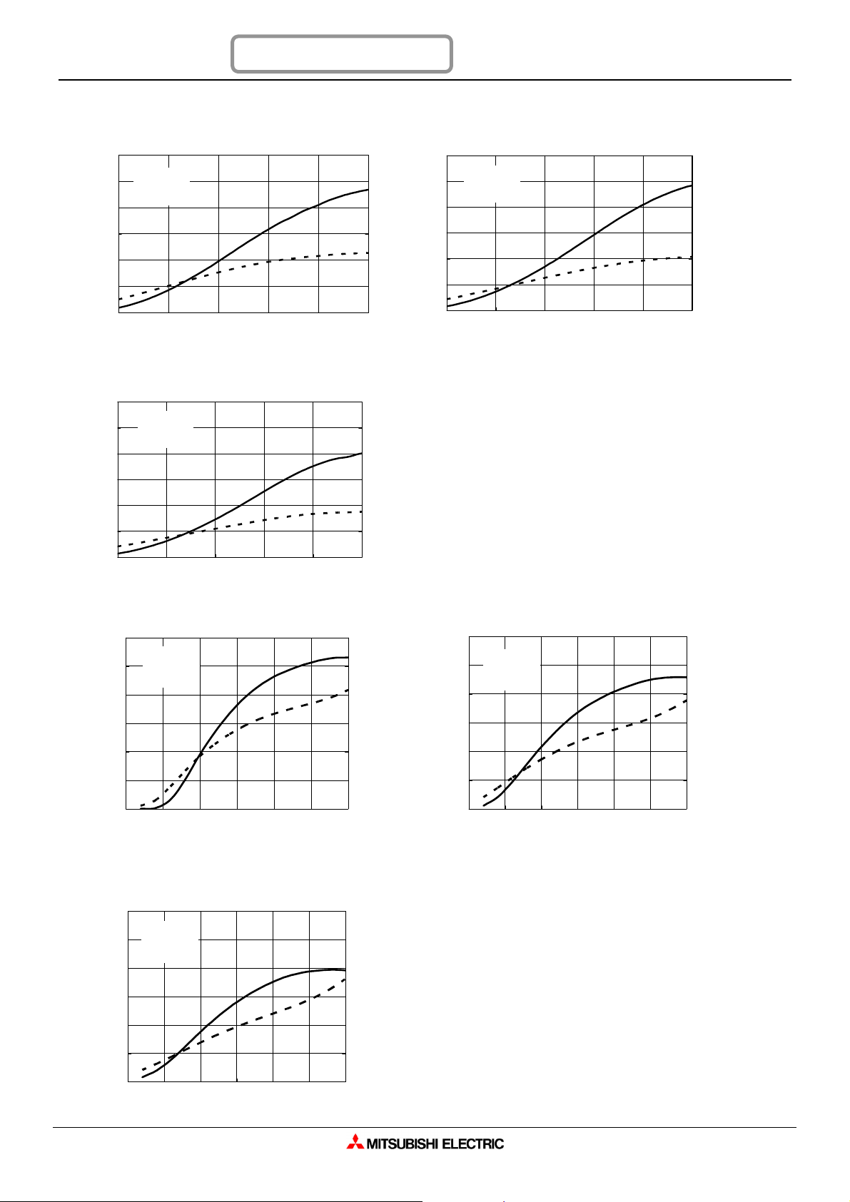
ELECTROSTATIC SENSITIVE DEVICE
OUTPUT POWER and DRAIN CURRENT
OUTPUT POWER and DRAIN CURRENT
versus GATE VOLTAGE
versus GATE VOLTAGE
OUTPUT POWER and DRAIN CURRENT
versus GATE VOLTAGE
OUTPUT POWER and DRAIN CURRENT
OUTPUT POWER and DRAIN CURRENT
versus DRAIN VOLTAGE
versus DRAIN VOLTAGE
OUTPUT POWER and DRAIN CURRENT
versus DRAIN VOLTAGE
OBSERVE HANDLING PRECAUTIONS
RoHS COMPLIANT
Silicon RF Power Semiconductors
RA01L8693MA
TYPICAL PERFORMANCE (T
6
f=865MHz,
5
VGG=2.0V,
(W)
Pin=30mW
out
4
3
2
1
OUTPUTPOWERP
0
1.0 2.0 3.0 4.0 5.0 6.0
6
5
(W)
out
4
3
2
1
OUTPUTPOWERP
0
1.0 2.0 3.0 4.0 5.0 6.0
P
out
DRAIN VOLTAGE VDD(V)
f=928MHz,
VGG=2.0V,
Pin=30mW
P
out
DRAIN VOLTAGE VDD(V)
=+25deg.C, ZG=ZL=50, unless otherwise specified)
case
6
5
4
3
I
I
DD
2
DD
1
0
6
5
(A)
4
DD
3
2
1
DRAINCURRENT I
0
6
f=900MHz,
5
VGG=2.0V,
(W)
Pin=30mW
out
(A)
4
DD
3
2
1
OUTPUTPOWERP
DRAINCURRENTI
0
1.0 2.0 3.0 4.0 5.0 6.0
P
out
DRAIN VOLTAGE VDD(V)
6
5
(A)
4
DD
3
2
I
DD
1
DRAINCURRENT I
0
3.0
f=865MHz,
2.5
(W)
out
2.0
VDD=3.3V,
Pin=30mW
P
out
1.5
I
DD
1.0
0.5
OUTPUTPOWER P
0.0
0.0 0.5 1.0 1.5 2.0 2.5 3.0
GATE VOLTAGE VGG(V)
3.0
f=928MHz,
2.5
2.0
VDD=3.3V,
Pin=30mW
P
out
(W)
out
1.5
1.0
I
3.0
2.5
2.0
1.5
1.0
0.5
0.0
3.0
P
f=900MHz,
2.5
(W)
(A)
DD
out
VDD=3.3V,
Pin=30mW
2.0
out
1.5
I
1.0
0.5
OUTPUTPOWER P
DD
DRAINCURRENT I
0.0
0.0 0.5 1.0 1.5 2.0 2.5 3.0
GATE VOLTAGE VGG(V)
3.0
2.5
2.0
1.5
1.0
0.5
0.0
(A)
DD
DRAIN CURRENT I
3.0
2.5
(A)
2.0
DD
1.5
DD
1.0
0.5
OUTPUTPOWER P
0.0
0.0 0.5 1.0 1.5 2.0 2.5 3.0
GATE VOLTAGE VGG(V)
RA01L8693MA 22 Jun 2010
0.5
DRAIN CURRENT I
0.0
4/12
Page 5

ELECTROSTATIC SENSITIVE DEVICE
OUTPUT POWER, POWER GAIN and
OUTPUT POWER, POWER GAIN and
DRAIN CURRENT versus INPUT POWER
DRAIN CURRENT versus INPUT POWER
OUTPUT POWER, POWER GAIN and
DRAIN CURRENT versus INPUT POWER
versus FREQUENCY
INPUT VSWR versus FREQUENCY
OBSERVE HANDLING PRECAUTIONS
RoHS COMPLIANT
Silicon RF Power Semiconductors
RA01L8693MA
TYPICAL PERFORMANCE (Vdd=5.0V,T
OUTPUT POWER, TOTAL EFFICIENCY, 2nd, 3rdHARMONICS versus FREQUENCY
5
P
4
(W)
out
3
2
OUTPUTPOWERP
1
0
850 860 870 880 890 900 910 920 930 940
5
4
(-)
in
r
3
2
INPUTVSWR
out
FREQUENCY f(MHz)
r
in
nT@Po=2W
VDD=5.0V
VGG=2.0V
VDD=5.0V
VGG=2.0V
Pin=30mW
=+25deg.C, ZG=ZL=50, unless otherwise specified)
case
50
45
40
35
30
25
20
15
TOTALEFFICIENCY(%)
10
5
0
-30
-35
-40
-45
-50
HARMONICS(dBc)
-55
-60
850 860 870 880 890 900 910 920 930 940
2nd
3rd
FREQUENCY f(MHz)
VDD=5.0V
VGG=2.0V
Pin=30mW
1
850 860 870 880 890 900 910 920 930 940
FREQUENCY f(MHz)
40
30
(dBm)
out
Gp
20
10
POWER GAIN Gp(dB)
OUTPUT POWERP
IDD
f=865MHz,
VDD=5.0V,
VGG=2.0V
0
-10 -5 0 5 10 15 20
INPUT POWER Pin(dBm)
40
30
(dBm)
out
Gp
P
out
4
(A)
3
DD
2
1
DRAIN CURRENT I
0
40
P
out
30
(dBm)
out
Gp
20
10
POWER GAIN Gp(dB)
OUTPUT POWERP
IDD
f=900MHz,
VDD=5.0V,
VGG=2.0V
0
4
(A)
3
DD
I
2
1
DRAIN CURRENT
0
-10 -5 0 5 10 15 20
INPUT POWER Pin(dBm)
4
P
out
(A)
3
DD
20
10
POWER GAIN Gp(dB)
OUTPUT POWERP
IDD
0
-10 -5 0 5 10 15 20
INPUT POWER Pin(dBm)
RA01L8693MA 22 Jun 2010
f=928MHz,
VDD=5.0V,
VGG=2.0V
2
1
DRAIN CURRENT I
0
5/12
Page 6

ELECTROSTATIC SENSITIVE DEVICE
OUTLINE
DRAWING
(mm)
9.2+/-0.2
OBSERVE HANDLING PRECAUTIONS
RoHS COMPLIANT
② ③
Silicon RF Power Semiconductors
RA01L8693MA
1 RF Input (Pin)
8.6+/-0.2
2 Gate Voltage (VGG)
8.0+/-0.2
3 Drain Voltage (VDD)
4.6+/-0.2
4 RF Output (P
2.55+/-0.2
5 RF Ground
⑤
out
)
9.1+/-0.2
8.6+/-0.1
7.6+/-0.2
①
④
4.2+/-0.2
5.6+/-0.2
7.8+/-0.2
INDEXMARK(Pin)
8.7+/-0.1
1.8+/-0.15
0.75+/-0.1
1 RF Input (Pin)
2 Gate Voltage (VGG)
3 Drain Voltage (VDD)
4 RF Output (P
5 RF Ground (Case)
out
)
RA01L8693MA 22 Jun 2010
6/12
Page 7

C1, C2
: 4700pF, 22uF in parallel
Power
Spectrum
Directional
ZG=50
Z
=50
C1
C2
TEST BLOCK DIAGRAM
514
3
2
ELECTROSTATIC SENSITIVE DEVICE
OBSERVE HANDLING PRECAUTIONS
RoHS COMPLIANT
Silicon RF Power Semiconductors
RA01L8693MA
Signal
Generator
Attenuator
Pre-
amplifier
Attenuator
Power
Meter
Coupler
- +
DC Power
Supply V
GG
DUT
+ -
DC Power
Supply V
Analyzer
Directional
Coupler
DD
Attenuator
Meter
1 RF Input (Pin)
2 Gate Voltage (VGG)
3 Drain Voltage (VDD)
4 RF Output (P
out
)
5 RF Ground
EQUIVALENT CIRCUIT
RA01L8693MA 22 Jun 2010
7/12
Page 8

ELECTROSTATIC SENSITIVE DEVICE
OBSERVE HANDLING PRECAUTIONS
RoHS COMPLIANT
Silicon RF Power Semiconductors
RA01L8693MA
RECOMMENDATIONS and APPLICATION INFORMATION:
Construction:
This module consists of an alumina substrate. For mechanical protection, a metal cap is attached (witch makes the
improvement of RF radiation easy).The MOSFET transistor chips are die bonded onto the substrate, wire bondedto
the substrate, and coated with resin. Lines on the substrate (eventually inductors), chip capacitors, and resistors
form the bias and matching circuits. The DC and RF connection is provided at the backside of substrate.
Following conditions must be avoided:
a) Bending forces on the alumina substrate (for example, by fast thermal changes)
b) Defluxing solvents reacting with the resin coating on the MOSFET chips (for example, Trichloroethylene)
c) Frequent on/off switching that causes thermal expansion of the resin
d) ESD, surge, over voltage in combination with load VSWR, and oscillation
ESD:
This MOSFET module is sensitive to ESD voltages down to 1000V. Appropriate ESD precautions are required.
Thermal Design of the Heat Sink:
At P
=1.4W, VDD=3.3V and Pin=30mW each stage transistor operating conditions are:
out
P
Stage
st
1
nd
2
in
(W)
0.03 0.3 57.2 0.115
0.3 1.4 7.6 1.00
The channel temperatures of each stage transistor Tch= T
T
= T
ch1
T
= T
ch2
+ (3.3V x 0.115A – 0.3W + 0.03W) x 57.2°C/W = T
case
+ (3.3V x 1.0A – 1.4W + 0.3W) x 7.6°C/W = T
case
P
out
(W)
R
th(ch-case)
(°C/W)
I
@ T=38%
DD
(A)
+ (VDDx IDD- P
case
V
DD
(V)
3.3
+ 6.3 °C
case
+ 16.7 °C
case
+ Pin) x R
out
th(ch-case)
are:
For long-term reliability, it is best to keep the module case temperature (T
temperature T
P
+ Pin) of the heat sink, including the contact resistance, is:
out
R
th(case-air)
=45°C and P
air
=1.4W, the required thermal resistance R
out
= (70°C - 45°C) / (1.4W/38% – 1.4W + 0.03W) = 10.8°C/W
) below 70°C. For an ambient
case
th (case-air)
= ( T
case
- T
) / ( (P
air
out
When mounting the module with the thermal resistance of 10.8°C/W, the channel temperature of each stage
transistor is:
T
= T
= T
+ 31.3 °C
air
+ 41.7 °C
air
ch1
T
ch2
The 150°C maximum rating for the channel temperature ensures application under derated conditions.
/ T) -
RA01L8693MA 22 Jun 2010
8/12
Page 9

ELECTROSTATIC SENSITIVE DEVICE
OBSERVE HANDLING PRECAUTIONS
RoHS COMPLIANT
Silicon RF Power Semiconductors
RA01L8693MA
Output Power Control:
The recommended method to control the output power is by the input power (Pin).
Oscillation:
To test RF characteristics, this module isput on a fixture with two bias decoupling capacitors each on gate and drain,
a 4.700 pF chip capacitor, located close to the module, and a 22 µF (or more) electrolytic capacitor.
When an amplifier circuit around this module shows oscillation, the following may be checked:
a) Do the bias decoupling capacitors have a low inductance pass to the case of the module?
b) Is the load impedance ZL=50
c) Is the source impedance ZG=50
ATTENTION:
1.High Temperature; This product might have a heat generation while operation,Please take notice that have a
possibility to receive a burn to touch the operating product directly or touch the product until cold after switch off.
At the near the product,do not place the combustible material that have possibilities to arise the fire.
2. Generation of High Frequency Power; This product generate a high frequency power. Please take notice that do
not leakage the unnecessary electric wave and use this products without cause damage for human and property per
normal operation.
3. Before use; Before use the product,Please design the equipment in consideration of the risk for human and
electric wave obstacle for equipment.
PRECAUTION FOR THE USE OF MITSUBISHI SILICON RF POWER AMPLIFIER DEVICES:
1.The specifications of mention are not guarantee values in this data sheet. Please confirm additional details
regarding operation of these products from the formal specification sheet. For copies of the formal specification
sheets, please contact one of our sales offices.
2.RAseries products(RF poweramplifier modules)are designed for consumer mobile communication terminals and
were not specifically designed for use in other applications. In particular, while these products are highly reliable
for their designed purpose, they are not manufactured under a quality assurance testing protocol that is sufficient
to guarantee the levelof reliabilitytypicallydeemed necessary for critical communications elements. Examples of
critical communications elements would include transmitters for base station applications and fixed station
applicationsthat operate withlongterm continuoustransmission anda higher on-off frequencyduring transmitting,
especially for systems that may have a high impact to society.
3.RA series products use MOSFET semiconductor technology. They are sensitive to ESD voltage therefore
appropriate ESD precautions are required.
4.In order to maximize reliability of the equipment, it is better to keep the devices temperature low. It is
recommended to utilize a sufficient sizedheat-sink in conjunction with other cooling methods as needed (fan, etc.)
to keep the case temperature for RA series products lower than 60deg/C under standard conditions, and less than
90deg/C under extreme conditions.
5.RA series products are designed to operate into a nominal load impedance of 50 ohms. Under the condition of
operating into a severe high load VSWR approaching an open or short, an over load condition could occur. In the
worst case there is risk for burn out of the transistors and burning of other parts including the substrate in the
module.
6.The formal specification includes a guarantee against parasitic oscillation under a specified maximum load
mismatch condition. The inspection for parasitic oscillation is performed on a sample basis on our manufacturing
line. It is recommended that verification of no parasitic oscillation be performed at the completed equipment level
also.
7.For specific precautions regarding assembly of these products into the equipment, please refer to the
supplementary items in the specification sheet.
8.Warranty for the product is void if the products protective cap (lid) is removed or if the product is modified in any
way from it’s original form.
9.For additional “Safety first” in your circuit design and notes regarding the materials, please refer the last page of
this data sheet.
10. Please refer to the additional precautions in the formal specification sheet.
RA01L8693MA 22 Jun 2010
9/12
Page 10

ELECTROSTATIC SENSITIVE DEVICE
OBSERVE HANDLING PRECAUTIONS
P.C.B Land Pattern Recommendation
8.60
8.00
4.60
③
2.55
②
4.20
④
①
Silicon RF Power Semiconductors
RoHS COMPLIANT
5.60
8.60
9.70
EQUILATERAL TRIANGLE ARRANGEMENT
RA01L8693MA
0.5
0
.
4
6
0
°
THROUGH HOLE
Mounting method
Mitsubishi recommends device mounting like Fig.1. In order to heat radiation, we recommend to fix
the PCB and heat sink by screw. This PCB has through holes that filled up with resin to restrain the
solder flow under the RF Ground. The interval of through holes is 0.4mm and these holes are
arranged in the shape of equilateral triangles.
Fig.1
Gate
RF Input
Fix with screws.
Reflow soldering
Drain
RF Ground
RF Output
Printed Circuit board
heat sink
# Note: Mitsubishi Heat Sink size=30 * 60 * 10 Unit: mm
RA01L8693MA 22 Jun 2010
10/12
Page 11

ELECTROSTATIC SENSITIVE DEVICE
OBSERVE HANDLING PRECAUTIONS
RoHS COMPLIANT
Silicon RF Power Semiconductors
RA01L8693MA
Reflow soldering
Regarding to reflow soldering, Mitsubishi recommend the heat profile of Fig.2. Reflow soldering is
able to do till 3 times.
Fig.2
Peak 255+0/-5℃MAX
10sec max
Temperature
175±10℃
110±20 sec
Time(sec)
above 200℃
70 sec max
RA01L8693MA 22 Jun 2010
11/12
Page 12

ELECTROSTATIC SENSITIVE DEVICE
any malfunction or mishap.
than the approved
destination.
OBSERVE HANDLING PRECAUTIONS
RoHS COMPLIANT
Silicon RF Power Semiconductors
RA01L8693MA
Keep safety first in your circuit designs !
MitsubishiElectric Corporation puts the maximum effort intomaking semiconductor products better and
more reliable, but there is always the possibility that trouble may occur with them. Trouble with
semiconductors may lead to personal injury, fire or property damage. Remember to give due
consideration to safety when making your circuit designs, with appropriate measures such as (i)
placement of substitutive, auxiliary circuits, (ii) use of non-flammable material or (iii) prevention against
Notes regarding these materials
- These materials are intended as a reference to assist our customers in the selection of the Mitsubishi
semiconductor product best suited to the customer’s application; they do not convey any license under
anyintellectual property rights, or any otherrights, belongingto Mitsubishi Electric Corporation or a third
party.
- Mitsubishi Electric Corporation assumes no responsibility for any damage, or infringement of any
third-party’s rights, originating in the use of any product data, diagrams, charts, programs, algorithms,
or circuit application examples contained in these materials.
- All information contained in these materials, including product data, diagrams, charts, programs and
algorithms represents information on products at the time of publication of these materials, and are
subject to change by Mitsubishi Electric Corporation without notice due to product improvements or
other reasons. It is therefore recommended that customers contact Mitsubishi Electric Corporation or
an authorized Mitsubishi Semiconductor product distributor for the latest product information before
purchasing a product listed herein. The information described here may contain technical inaccuracies
or typographical errors. Mitsubishi Electric Corporation assumes no responsibility for any damage,
liability, or other loss rising from these inaccuracies or errors. Please also pay attention to information
published by MitsubishiElectric Corporation by various means, including the Mitsubishi Semiconductor
home page (http://www.mitsubishichips.com).
- When using anyor all of the information contained in these materials, including product data, diagrams,
charts, programs, and algorithms, please be sure to evaluate all information as a total system before
making a final decision on the applicability of the information and products. Mitsubishi Electric
Corporation assumes no responsibility for any damage, liability or other loss resulting from the
information contained herein.
- Mitsubishi Electric Corporation semiconductors are not designed or manufactured for use in a device or
system that is used under circumstances in which human life is potentially at stake. Please contact
Mitsubishi Electric Corporation or an authorized Mitsubishi Semiconductor product distributor when
considering the use of a product contained herein for any specific purposes, such as apparatus or
systems for transportation, vehicular, medical, aerospace, nuclear, or undersea repeater use.
- The prior written approval of Mitsubishi Electric Corporationis necessaryto reprint or reproduce in whole
or in part these materials.
- If these products or technologies are subject to the Japanese export control restrictions, they must be
exported under a license from the Japanese government and cannot be imported into a country other
RA01L8693MA 22 Jun 2010
12/12
 Loading...