

Page 1

MELSEC iQ-R Digital-Analog Converter Module
User's Manual (Application)
-R60DA4
-R60DAV8
-R60DAI8
Page 2

Page 3
SAFETY PRECAUTIONS
WARNING
Indicates that incorrect handling may cause hazardous conditions, resulting in
death or severe injury.
CAUTION
Indicates that incorrect handling may cause hazardous conditions, resulting in
minor or moderate injury or property damage.
(Read these precautions before using this product.)
Before using this product, please read this manual and the relevant manuals carefully and pay full attention to safety to handle
the product correctly.
The precautions given in this manual are concerned with this product only. For the safety precautions of the programmable
controller system, refer to the MELSEC iQ-R Module Configuration Manual.
In this manual, the safety precautions are classified into two levels: " WARNING" and " CAUTION".
Under some circumstances, failure to observe the precautions given under " CAUTION" may lead to serious
consequences.
Observe the precautions of both levels because they are important for personal and system safety.
Make sure that the end users read this manual and then keep the manual in a safe place for future reference.
1
Page 4

[Design Precautions]
WARNING
● Configure safety circuits external to the programmable controller to ensure that the entire system
operates safely even when a fault occurs in the external power supply or the programmable controller.
Failure to do so may result in an accident due to an incorrect output or malfunction.
(1) Emergency stop circuits, protection circuits, and protective interlock circuits for conflicting
operations (such as forward/reverse rotations or upper/lower limit positioning) must be configured
external to the programmable controller.
(2) When the programmable controller detects an abnormal condition, it stops the operation and all
outputs are:
• Turned off if the overcurrent or overvoltage protection of the power supply module is activated.
• Held or turned off according to the parameter setting if the self-diagnostic function of the CPU
module detects an error such as a watchdog timer error.
(3) All outputs may be turned on if an error occurs in a part, such as an I/O control part, where the
CPU module cannot detect any error. To ensure safety operation in such a case, provide a safety
mechanism or a fail-safe circuit external to the programmable controller. For a fail-safe circuit
example, refer to "General Safety Requirements" in the MELSEC iQ-R Module Configuration
Manual.
(4) Outputs may remain on or off due to a failure of a component such as a relay and transistor in an
output circuit. Configure an external circuit for monitoring output signals that could cause a
serious accident.
● In an output circuit, when a load current exceeding the rated current or an overcurrent caused by a
load short-circuit flows for a long time, it may cause smoke and fire. To prevent this, configure an
external safety circuit, such as a fuse.
● Configure a circuit so that the programmable controller is turned on first and then the external power
supply. If the external power supply is turned on first, an accident may occur due to an incorrect output
or malfunction.
● For the operating status of each station after a communication failure, refer to manuals relevant to the
network. Incorrect output or malfunction due to a communication failure may result in an accident.
● When connecting an external device with a CPU module or intelligent function module to modify data
of a running programmable controller, configure an interlock circuit in the program to ensure that the
entire system will always operate safely. For other forms of control (such as program modification,
parameter change, forced output, or operating status change) of a running programmable controller,
read the relevant manuals carefully and ensure that the operation is safe before proceeding. Improper
operation may damage machines or cause accidents.
● Especially, when a remote programmable controller is controlled by an external device, immediate
action cannot be taken if a problem occurs in the programmable controller due to a communication
failure. To prevent this, configure an interlock circuit in the program, and determine corrective actions
to be taken between the external device and CPU module in case of a communication failure.
● Do not write any data to the "system area" and "write-protect area" of the buffer memory in the
module. Also, do not use any "use prohibited" signals as an output signal from the CPU module to
each module. Doing so may cause malfunction of the programmable controller system. For the
"system area", "write-protect area", and the "use prohibited" signals, refer to the user's manual for the
module used.
2
Page 5
[Design Precautions]
WARNING
● If a communication cable is disconnected, the network may be unstable, resulting in a communication
failure of multiple stations. Configure an interlock circuit in the program to ensure that the entire
system will always operate safely even if communications fail. Incorrect output or malfunction due to a
communication failure may result in an accident.
● To maintain the safety of the programmable controller system against unauthorized access from
external devices via the network, take appropriate measures. To maintain the safety against
unauthorized access via the Internet, take measures such as installing a firewall.
● Analog outputs may remain on due to a failure of the module. Configure an external interlock circuit
for output signals that could cause a serious accident.
[Design Precautions]
CAUTION
● Do not install the control lines or communication cables together with the main circuit lines or power
cables. Keep a distance of 100mm or more between them. Failure to do so may result in malfunction
due to noise.
● During control of an inductive load such as a lamp, heater, or solenoid valve, a large current
(approximately ten times greater than normal) may flow when the output is turned from off to on.
Therefore, use a module that has a sufficient current rating.
● After the CPU module is powered on or is reset, the time taken to enter the RUN status varies
depending on the system configuration, parameter settings, and/or program size. Design circuits so
that the entire system will always operate safely, regardless of the time.
● Do not power off the programmable controller or reset the CPU module while the setting values in the
buffer memory are being written to the flash ROM in the module. Doing so will make the data in the
flash ROM undefined. The values need to be set in the buffer memory and written to the flash ROM
again. Doing so also can cause malfunction or failure of the module.
● When changing the operating status of the CPU module (such as remote RUN/STOP) from the
external device, select "Do Not OPEN in Program" for the "Open Method Setting" in the module
parameter. The communication line will be closed when "OPEN in Program" is selected and the
remote STOP is executed from the external device. Consequently, the CPU module cannot reopen
the communication line, and the external device cannot execute the remote RUN.
● Power on or off the external power supply while the programmable controller is on. Failure to do so
may result in incorrect output or malfunction.
● At on/off of the power or external power supply, or at the output range switching, a voltage may occur
or a current may flow between output terminals for a moment. In this case, start the control after
analog outputs become stable.
3
Page 6
[Installation Precautions]
WARNING
● Shut off the external power supply (all phases) used in the system before mounting or removing the
module. Failure to do so may result in electric shock or cause the module to fail or malfunction.
[Installation Precautions]
CAUTION
● Use the programmable controller in an environment that meets the general specifications in the Safety
Guidelines included with the base unit. Failure to do so may result in electric shock, fire, malfunction,
or damage to or deterioration of the product.
● To mount a module, place the concave part(s) located at the bottom onto the guide(s) of the base unit,
and push in the module until the hook(s) located at the top snaps into place. Incorrect interconnection
may cause malfunction, failure, or drop of the module.
● When using the programmable controller in an environment of frequent vibrations, fix the module with
a screw.
● Tighten the screws within the specified torque range. Undertightening can cause drop of the screw,
short circuit, or malfunction. Overtightening can damage the screw and/or module, resulting in drop,
short circuit, or malfunction.
● When using an extension cable, connect it to the extension cable connector of the base unit securely.
Check the connection for looseness. Poor contact may cause malfunction.
● When using an SD memory card, fully insert it into the SD memory card slot. Check that it is inserted
completely. Poor contact may cause malfunction. / Failure to do so may cause malfunction.
● Securely insert an extended SRAM cassette into the cassette connector of the CPU module. After
insertion, close the cassette cover and check that the cassette is inserted completely. Poor contact
may cause malfunction.
● Do not directly touch any conductive parts and electronic components of the module, SD memory
card, extended SRAM cassette, or connector. Doing so can cause malfunction or failure of the
module.
[Wiring Precautions]
WARNING
● Shut off the external power supply (all phases) used in the system before installation or wiring. Failure
to do so may result in electric shock or cause the module to fail or malfunction.
● After installation and wiring, attach the included terminal cover to the module before turning it on for
operation. Failure to do so may result in electric shock.
4
Page 7

[Wiring Precautions]
CAUTION
● Individually ground the FG and LG terminals of the programmable controller with a ground resistance
of 100 ohms or less. Failure to do so may result in electric shock or malfunction.
● Use applicable solderless terminals and tighten them within the specified torque range. If any spade
solderless terminal is used, it may be disconnected when the terminal screw comes loose, resulting in
failure.
● Check the rated voltage and signal layout before wiring to the module, and connect the cables
correctly. Connecting a power supply with a different voltage rating or incorrect wiring may cause fire
or failure.
● Connectors for external devices must be crimped or pressed with the tool specified by the
manufacturer, or must be correctly soldered. Incomplete connections may cause short circuit, fire, or
malfunction.
● Securely connect the connector to the module. Poor contact may cause malfunction.
● Do not install the control lines or communication cables together with the main circuit lines or power
cables. Keep a distance of 100mm or more between them. Failure to do so may result in malfunction
due to noise.
● Place the cables in a duct or clamp them. If not, dangling cable may swing or inadvertently be pulled,
resulting in damage to the module or cables or malfunction due to poor contact. Do not clamp the
extension cables with the jacket stripped. Doing so may change the characteristics of the cables,
resulting in malfunction.
● Check the interface type and correctly connect the cable. Incorrect wiring (connecting the cable to an
incorrect interface) may cause failure of the module and external device.
● Tighten the terminal screws or connector screws within the specified torque range. Undertightening
can cause drop of the screw, short circuit, fire, or malfunction. Overtightening can damage the screw
and/or module, resulting in drop, short circuit, fire, or malfunction.
● When disconnecting the cable from the module, do not pull the cable by the cable part. For the cable
with connector, hold the connector part of the cable. For the cable connected to the terminal block,
loosen the terminal screw. Pulling the cable connected to the module may result in malfunction or
damage to the module or cable.
● Prevent foreign matter such as dust or wire chips from entering the module. Such foreign matter can
cause a fire, failure, or malfunction.
● A protective film is attached to the top of the module to prevent foreign matter, such as wire chips,
from entering the module during wiring. Do not remove the film during wiring. Remove it for heat
dissipation before system operation.
● Mitsubishi programmable controllers must be installed in control panels. Connect the main power
supply to the power supply module in the control panel through a relay terminal block. Wiring and
replacement of a power supply module must be performed by qualified maintenance personnel with
knowledge of protection against electric shock. For wiring, refer to the MELSEC iQ-R Module
Configuration Manual.
● For Ethernet cables to be used in the system, select the ones that meet the specifications in the user's
manual for each module. If not, normal data transmission is not guaranteed.
5
Page 8

[Startup and Maintenance Precautions]
Warning
● Do not touch any terminal while power is on. Doing so will cause electric shock or malfunction.
● Correctly connect the battery connector. Do not charge, disassemble, heat, short-circuit, solder, or
throw the battery into the fire. Also, do not expose it to liquid or strong shock. Doing so will cause the
battery to produce heat, explode, ignite, or leak, resulting in injury and fire.
● Shut off the external power supply (all phases) used in the system before cleaning the module or
retightening the terminal screws, connector screws, or module fixing screws. Failure to do so may
result in electric shock.
6
Page 9

[Startup and Maintenance Precautions]
CAUTION
● When connecting an external device with a CPU module or intelligent function module to modify data
of a running programmable controller, configure an interlock circuit in the program to ensure that the
entire system will always operate safely. For other forms of control (such as program modification,
parameter change, forced output, or operating status change) of a running programmable controller,
read the relevant manuals carefully and ensure that the operation is safe before proceeding. Improper
operation may damage machines or cause accidents.
● Especially, when a remote programmable controller is controlled by an external device, immediate
action cannot be taken if a problem occurs in the programmable controller due to a communication
failure. To prevent this, configure an interlock circuit in the program, and determine corrective actions
to be taken between the external device and CPU module in case of a communication failure.
● Do not disassemble or modify the modules. Doing so may cause failure, malfunction, injury, or a fire.
● Use any radio communication device such as a cellular phone or PHS (Personal Handy-phone
System) more than 25cm away in all directions from the programmable controller. Failure to do so
may cause malfunction.
● Shut off the external power supply (all phases) used in the system before mounting or removing the
module. Failure to do so may cause the module to fail or malfunction.
● Tighten the screws within the specified torque range. Undertightening can cause drop of the
component or wire, short circuit, or malfunction. Overtightening can damage the screw and/or module,
resulting in drop, short circuit, or malfunction.
● After the first use of the product, do not mount/remove the module to/from the base unit, and the
terminal block to/from the module, and do not insert/remove the extended SRAM cassette to/from the
CPU module more than 50 times (IEC 61131-2 compliant) respectively. Exceeding the limit may cause
malfunction.
● After the first use of the product, do not insert/remove the SD memory card to/from the CPU module
more than 500 times. Exceeding the limit may cause malfunction.
● Do not touch the metal terminals on the back side of the SD memory card. Doing so may cause
malfunction.
● Do not touch the integrated circuits on the circuit board of an extended SRAM cassette. Doing so may
cause malfunction.
● Do not drop or apply shock to the battery to be installed in the module. Doing so may damage the
battery, causing the battery fluid to leak inside the battery. If the battery is dropped or any shock is
applied to it, dispose of it without using.
● Startup and maintenance of a control panel must be performed by qualified maintenance personnel
with knowledge of protection against electric shock. Lock the control panel so that only qualified
maintenance personnel can operate it.
● Before handling the module, touch a conducting object such as a grounded metal to discharge the
static electricity from the human body. Failure to do so may cause the module to fail or malfunction.
7
Page 10
[Operating Precautions]
CAUTION
● When changing data and operating status, and modifying program of the running programmable
controller from an external device such as a personal computer connected to an intelligent function
module, read relevant manuals carefully and ensure the safety before operation. Incorrect change or
modification may cause system malfunction, damage to the machines, or accidents.
● Do not power off the programmable controller or reset the CPU module while the setting values in the
buffer memory are being written to the flash ROM in the module. Doing so will make the data in the
flash ROM undefined. The values need to be set in the buffer memory and written to the flash ROM
again. Doing so also can cause malfunction or failure of the module.
[Disposal Precautions]
CAUTION
● When disposing of this product, treat it as industrial waste.
● When disposing of batteries, separate them from other wastes according to the local regulations. For
details on battery regulations in EU member states, refer to the MELSEC iQ-R Module Configuration
Manual.
[Transportation Precautions]
CAUTION
● When transporting lithium batteries, follow the transportation regulations. For details on the regulated
models, refer to the MELSEC iQ-R Module Configuration Manual.
● The halogens (such as fluorine, chlorine, bromine, and iodine), which are contained in a fumigant
used for disinfection and pest control of wood packaging materials, may cause failure of the product.
Prevent the entry of fumigant residues into the product or consider other methods (such as heat
treatment) instead of fumigation. The disinfection and pest control measures must be applied to
unprocessed raw wood.
8
Page 11

CONDITIONS OF USE FOR THE PRODUCT
(1) Mitsubishi programmable controller ("the PRODUCT") shall be used in conditions;
i) where any problem, fault or failure occurring in the PRODUCT, if any, shall not lead to any major or serious accident;
and
ii) where the backup and fail-safe function are systematically or automatically provided outside of the PRODUCT for the
case of any problem, fault or failure occurring in the PRODUCT.
(2) The PRODUCT has been designed and manufactured for the purpose of being used in general industries.
MITSUBISHI SHALL HAVE NO RESPONSIBILITY OR LIABILITY (INCLUDING, BUT NOT LIMITED TO ANY AND ALL
RESPONSIBILITY OR LIABILITY BASED ON CONTRACT, WARRANTY, TORT, PRODUCT LIABILITY) FOR ANY
INJURY OR DEATH TO PERSONS OR LOSS OR DAMAGE TO PROPERTY CAUSED BY the PRODUCT THAT ARE
OPERATED OR USED IN APPLICATION NOT INTENDED OR EXCLUDED BY INSTRUCTIONS, PRECAUTIONS, OR
WARNING CONTAINED IN MITSUBISHI'S USER, INSTRUCTION AND/OR SAFETY MANUALS, TECHNICAL
BULLETINS AND GUIDELINES FOR the PRODUCT.
("Prohibited Application")
Prohibited Applications include, but not limited to, the use of the PRODUCT in;
• Nuclear Power Plants and any other power plants operated by Power companies, and/or any other cases in which the
public could be affected if any problem or fault occurs in the PRODUCT.
• Railway companies or Public service purposes, and/or any other cases in which establishment of a special quality
assurance system is required by the Purchaser or End User.
• Aircraft or Aerospace, Medical applications, Train equipment, transport equipment such as Elevator and Escalator,
Incineration and Fuel devices, Vehicles, Manned transportation, Equipment for Recreation and Amusement, and
Safety devices, handling of Nuclear or Hazardous Materials or Chemicals, Mining and Drilling, and/or other
applications where there is a significant risk of injury to the public or property.
Notwithstanding the above restrictions, Mitsubishi may in its sole discretion, authorize use of the PRODUCT in one or
more of the Prohibited Applications, provided that the usage of the PRODUCT is limited only for the specific
applications agreed to by Mitsubishi and provided further that no special quality assurance or fail-safe, redundant or
other safety features which exceed the general specifications of the PRODUCTs are required. For details, please
contact the Mitsubishi representative in your region.
9
Page 12

INTRODUCTION
Thank you for purchasing the Mitsubishi Electric MELSEC iQ-R series programmable controllers.
This manual describes the functions, parameter settings, and troubleshooting of the relevant products listed below.
Before using this product, please read this manual and the relevant manuals carefully and develop familiarity with the
functions and performance of the MELSEC iQ-R series programmable controller to handle the product correctly.
When applying the program examples provided in this manual to an actual system, ensure the applicability and confirm that it
will not cause system control problems.
Please make sure that the end users read this manual.
Unless otherwise specified, this manual describes the program examples in which the I/O numbers of X/Y0 to
X/YF are assigned for a D/A converter module. I/O numbers must be assigned to apply the program examples
introduced in this manual to an actual system. For I/O number assignment, refer to the following.
MELSEC iQ-R CPU Module User's Manual (Application)
Relevant products
R60DA4. R60DAV8, R60DAI8
10
Page 13

MEMO
11
Page 14

CONTENTS
SAFETY PRECAUTIONS . . . . . . . . . . . . . . . . . . . . . . . . . . . . . . . . . . . . . . . . . . . . . . . . . . . . . . . . . . . . . . . . . . . .1
CONDITIONS OF USE FOR THE PRODUCT . . . . . . . . . . . . . . . . . . . . . . . . . . . . . . . . . . . . . . . . . . . . . . . . . . . .9
INTRODUCTION. . . . . . . . . . . . . . . . . . . . . . . . . . . . . . . . . . . . . . . . . . . . . . . . . . . . . . . . . . . . . . . . . . . . . . . . . .10
RELEVANT MANUALS . . . . . . . . . . . . . . . . . . . . . . . . . . . . . . . . . . . . . . . . . . . . . . . . . . . . . . . . . . . . . . . . . . . . .14
TERMS . . . . . . . . . . . . . . . . . . . . . . . . . . . . . . . . . . . . . . . . . . . . . . . . . . . . . . . . . . . . . . . . . . . . . . . . . . . . . . . . .14
CHAPTER 1 FUNCTIONS 15
1.1 Modes . . . . . . . . . . . . . . . . . . . . . . . . . . . . . . . . . . . . . . . . . . . . . . . . . . . . . . . . . . . . . . . . . . . . . . . . . . . . . . . . .16
1.2 Range Switching Function . . . . . . . . . . . . . . . . . . . . . . . . . . . . . . . . . . . . . . . . . . . . . . . . . . . . . . . . . . . . . . . .18
1.3 D/A Conversion Enable/Disable Function . . . . . . . . . . . . . . . . . . . . . . . . . . . . . . . . . . . . . . . . . . . . . . . . . . . . 19
1.4 D/A Output Enable/Disable Setting Function . . . . . . . . . . . . . . . . . . . . . . . . . . . . . . . . . . . . . . . . . . . . . . . . .19
1.5 Analog Output HOLD/CLEAR Function. . . . . . . . . . . . . . . . . . . . . . . . . . . . . . . . . . . . . . . . . . . . . . . . . . . . . .20
1.6 Analog Output Test when CPU Module is in STOP Status Function . . . . . . . . . . . . . . . . . . . . . . . . . . . . . . 22
1.7 Scaling Function . . . . . . . . . . . . . . . . . . . . . . . . . . . . . . . . . . . . . . . . . . . . . . . . . . . . . . . . . . . . . . . . . . . . . . . .23
1.8 Shift Function . . . . . . . . . . . . . . . . . . . . . . . . . . . . . . . . . . . . . . . . . . . . . . . . . . . . . . . . . . . . . . . . . . . . . . . . . . 26
1.9 Alert Output Function . . . . . . . . . . . . . . . . . . . . . . . . . . . . . . . . . . . . . . . . . . . . . . . . . . . . . . . . . . . . . . . . . . . . 28
1.10 Rate Control Function. . . . . . . . . . . . . . . . . . . . . . . . . . . . . . . . . . . . . . . . . . . . . . . . . . . . . . . . . . . . . . . . . . . .30
1.11 External Power Supply Disconnection Detection Function . . . . . . . . . . . . . . . . . . . . . . . . . . . . . . . . . . . . . 33
1.12 Disconnection Detection Function . . . . . . . . . . . . . . . . . . . . . . . . . . . . . . . . . . . . . . . . . . . . . . . . . . . . . . . . .34
1.13 Interrupt Function . . . . . . . . . . . . . . . . . . . . . . . . . . . . . . . . . . . . . . . . . . . . . . . . . . . . . . . . . . . . . . . . . . . . . . .35
1.14 Wave Output Function . . . . . . . . . . . . . . . . . . . . . . . . . . . . . . . . . . . . . . . . . . . . . . . . . . . . . . . . . . . . . . . . . . . 38
Initial settings of the wave output function. . . . . . . . . . . . . . . . . . . . . . . . . . . . . . . . . . . . . . . . . . . . . . . . . . . . . .46
Execution of the wave output function. . . . . . . . . . . . . . . . . . . . . . . . . . . . . . . . . . . . . . . . . . . . . . . . . . . . . . . . .52
Points to use the wave output function . . . . . . . . . . . . . . . . . . . . . . . . . . . . . . . . . . . . . . . . . . . . . . . . . . . . . . . .64
Wave output step action function . . . . . . . . . . . . . . . . . . . . . . . . . . . . . . . . . . . . . . . . . . . . . . . . . . . . . . . . . . . . 70
1.15 Inter-Module Synchronization Function . . . . . . . . . . . . . . . . . . . . . . . . . . . . . . . . . . . . . . . . . . . . . . . . . . . . . 78
1.16 Error History Function . . . . . . . . . . . . . . . . . . . . . . . . . . . . . . . . . . . . . . . . . . . . . . . . . . . . . . . . . . . . . . . . . . .84
1.17 Event History Function . . . . . . . . . . . . . . . . . . . . . . . . . . . . . . . . . . . . . . . . . . . . . . . . . . . . . . . . . . . . . . . . . . .87
1.18 Backing up, Saving, and Restoring Offset/Gain Values . . . . . . . . . . . . . . . . . . . . . . . . . . . . . . . . . . . . . . . . 88
When a module-specific backup parameters is used . . . . . . . . . . . . . . . . . . . . . . . . . . . . . . . . . . . . . . . . . . . . .88
When the module-specific backup parameter is not used. . . . . . . . . . . . . . . . . . . . . . . . . . . . . . . . . . . . . . . . . .90
1.19 Q Compatible Mode Function. . . . . . . . . . . . . . . . . . . . . . . . . . . . . . . . . . . . . . . . . . . . . . . . . . . . . . . . . . . . . .94
12
CHAPTER 2 PARAMETER SETTING 95
2.1 Basic Setting . . . . . . . . . . . . . . . . . . . . . . . . . . . . . . . . . . . . . . . . . . . . . . . . . . . . . . . . . . . . . . . . . . . . . . . . . . .95
2.2 Application Setting . . . . . . . . . . . . . . . . . . . . . . . . . . . . . . . . . . . . . . . . . . . . . . . . . . . . . . . . . . . . . . . . . . . . . . 96
2.3 Interrupt Setting. . . . . . . . . . . . . . . . . . . . . . . . . . . . . . . . . . . . . . . . . . . . . . . . . . . . . . . . . . . . . . . . . . . . . . . . .97
2.4 Refresh Settings . . . . . . . . . . . . . . . . . . . . . . . . . . . . . . . . . . . . . . . . . . . . . . . . . . . . . . . . . . . . . . . . . . . . . . . .98
Refresh processing time . . . . . . . . . . . . . . . . . . . . . . . . . . . . . . . . . . . . . . . . . . . . . . . . . . . . . . . . . . . . . . . . . . . 99
CHAPTER 3 TROUBLESHOOTING 100
3.1 Checking Using LEDs . . . . . . . . . . . . . . . . . . . . . . . . . . . . . . . . . . . . . . . . . . . . . . . . . . . . . . . . . . . . . . . . . . . 100
3.2 Checking the Status of the Module . . . . . . . . . . . . . . . . . . . . . . . . . . . . . . . . . . . . . . . . . . . . . . . . . . . . . . . . 101
3.3 Troubleshooting by Symptom . . . . . . . . . . . . . . . . . . . . . . . . . . . . . . . . . . . . . . . . . . . . . . . . . . . . . . . . . . . . 102
When the RUN LED flashes or turns off . . . . . . . . . . . . . . . . . . . . . . . . . . . . . . . . . . . . . . . . . . . . . . . . . . . . . . 102
When the ERR LED turns on. . . . . . . . . . . . . . . . . . . . . . . . . . . . . . . . . . . . . . . . . . . . . . . . . . . . . . . . . . . . . . .102
When the ALM LED turns on. . . . . . . . . . . . . . . . . . . . . . . . . . . . . . . . . . . . . . . . . . . . . . . . . . . . . . . . . . . . . . . 102
When an analog value is not output . . . . . . . . . . . . . . . . . . . . . . . . . . . . . . . . . . . . . . . . . . . . . . . . . . . . . . . . . 103
Page 15

When an analog value is not output with the wave output function being selected. . . . . . . . . . . . . . . . . . . . . .104
When HOLD of analog output value is not available. . . . . . . . . . . . . . . . . . . . . . . . . . . . . . . . . . . . . . . . . . . . . 104
When the synchronization output is not performed . . . . . . . . . . . . . . . . . . . . . . . . . . . . . . . . . . . . . . . . . . . . . .105
When 'External power supply READY flag' (X7) does not turn on . . . . . . . . . . . . . . . . . . . . . . . . . . . . . . . . . . 105
3.4 Error Code List . . . . . . . . . . . . . . . . . . . . . . . . . . . . . . . . . . . . . . . . . . . . . . . . . . . . . . . . . . . . . . . . . . . . . . . .106
3.5 Alarm Code List. . . . . . . . . . . . . . . . . . . . . . . . . . . . . . . . . . . . . . . . . . . . . . . . . . . . . . . . . . . . . . . . . . . . . . . . 110
APPENDICES 111
Appendix 1 Module Label . . . . . . . . . . . . . . . . . . . . . . . . . . . . . . . . . . . . . . . . . . . . . . . . . . . . . . . . . . . . . . . . . . . . . 111
Appendix 2 I/O Signals . . . . . . . . . . . . . . . . . . . . . . . . . . . . . . . . . . . . . . . . . . . . . . . . . . . . . . . . . . . . . . . . . . . . . . . 113
List of I/O signals. . . . . . . . . . . . . . . . . . . . . . . . . . . . . . . . . . . . . . . . . . . . . . . . . . . . . . . . . . . . . . . . . . . . . . . . 113
Details of input signals. . . . . . . . . . . . . . . . . . . . . . . . . . . . . . . . . . . . . . . . . . . . . . . . . . . . . . . . . . . . . . . . . . . . 114
Details of output signals . . . . . . . . . . . . . . . . . . . . . . . . . . . . . . . . . . . . . . . . . . . . . . . . . . . . . . . . . . . . . . . . . .121
Appendix 3 Buffer Memory . . . . . . . . . . . . . . . . . . . . . . . . . . . . . . . . . . . . . . . . . . . . . . . . . . . . . . . . . . . . . . . . . . . .124
List of buffer memory addresses . . . . . . . . . . . . . . . . . . . . . . . . . . . . . . . . . . . . . . . . . . . . . . . . . . . . . . . . . . . .124
Details of buffer memory addresses . . . . . . . . . . . . . . . . . . . . . . . . . . . . . . . . . . . . . . . . . . . . . . . . . . . . . . . . .136
Appendix 4 Dedicated Instruction . . . . . . . . . . . . . . . . . . . . . . . . . . . . . . . . . . . . . . . . . . . . . . . . . . . . . . . . . . . . . .174
Instruction list. . . . . . . . . . . . . . . . . . . . . . . . . . . . . . . . . . . . . . . . . . . . . . . . . . . . . . . . . . . . . . . . . . . . . . . . . . . 174
Appendix 5 Operation Examples of When the Remote Head Module Is Mounted . . . . . . . . . . . . . . . . . . . . . . . .175
System configuration example . . . . . . . . . . . . . . . . . . . . . . . . . . . . . . . . . . . . . . . . . . . . . . . . . . . . . . . . . . . . .175
Setting in the master station . . . . . . . . . . . . . . . . . . . . . . . . . . . . . . . . . . . . . . . . . . . . . . . . . . . . . . . . . . . . . . .176
Setting in the intelligent device station . . . . . . . . . . . . . . . . . . . . . . . . . . . . . . . . . . . . . . . . . . . . . . . . . . . . . . .179
Checking the network status . . . . . . . . . . . . . . . . . . . . . . . . . . . . . . . . . . . . . . . . . . . . . . . . . . . . . . . . . . . . . . . 182
Program examples . . . . . . . . . . . . . . . . . . . . . . . . . . . . . . . . . . . . . . . . . . . . . . . . . . . . . . . . . . . . . . . . . . . . . . 182
Appendix 6 Added or Changed Functions. . . . . . . . . . . . . . . . . . . . . . . . . . . . . . . . . . . . . . . . . . . . . . . . . . . . . . . . 185
CONTENTS
INDEX 186
REVISIONS. . . . . . . . . . . . . . . . . . . . . . . . . . . . . . . . . . . . . . . . . . . . . . . . . . . . . . . . . . . . . . . . . . . . . . . . . . . . .188
WARRANTY . . . . . . . . . . . . . . . . . . . . . . . . . . . . . . . . . . . . . . . . . . . . . . . . . . . . . . . . . . . . . . . . . . . . . . . . . . . .189
TRADEMARK . . . . . . . . . . . . . . . . . . . . . . . . . . . . . . . . . . . . . . . . . . . . . . . . . . . . . . . . . . . . . . . . . . . . . . . . . . .190
13
Page 16
RELEVANT MANUALS
Manual name [manual number] Description Available form
MELSEC iQ-R Digital-Analog Converter Module User's
Manual (Application)
[SH-081237ENG] (this manual)
MELSEC iQ-R Digital-Analog Converter Module User's
Manual (Startup)
[SH-081235ENG]
MELSEC iQ-R Programming Manual (Module Dedicated
Instructions)
[SH-081976ENG]
e-Manuals are electronic book-type manuals for Mitsubishi Electric FA products that can be read with a
dedicated tool.
The following shows the features of e-Manuals.
• Desired information can be searched for from multiple manuals at a time. (Manual cross search)
• Other manuals can be referred to from links in a manual.
• Desired hardware specifications can be checked from each part in the illustrations of products.
• Information frequently referred to can be registered as a favorite.
• Sample programs can be copied to an engineering tool.
Functions, parameter setting, troubleshooting, I/O signals, and buffer
memory of the D/A converter module
Specifications, procedures before operation, wiring, operatio n example,
and offset/gain setting of the D/A converter module
Dedicated instructions for the intelligent function modules e-Manual
Print book
e-Manual
PDF
Print book
e-Manual
PDF
PDF
TERMS
Unless otherwise specified, this manual uses the following terms.
Term Description
D/A converter module The abbreviation for the MELSEC iQ-R series digital-analog converter module
GX Works3 The product name of the software package for the MELSEC programmable controllers
Watchdog timer error An error that occurs if the internal processing of the D/A converter module is abnormal. Watchdog timer enables
Engineering tool A generic term for GX Works3
Factory default setting A generic term for analog output ranges of 0 to 10V, 0 to 5V, 1 to 5V, -10 to 10V, 0 to 20mA, and 4 to 20mA
Normal mode Setting values of the operation mode setting: normal mode and offset/gain setting mode
Offset/gain setting mode
Synchronization normal output mode When the inter-module synchronization function target is enabled, a value is set to CH Synchronization digital
Buffer memory A memory in an intelligent function module, where data (such as setting values and monitoring values)
User range An analog output range where any value can be set. Set the user range in the offset/gain setting.
R mode A mode that the module operates w ith the buffer memory map that memory areas have been newly laid out in the
Q compatible mode A mode that the module operates with the buffer memory map converted to the equivalent map of the MELSEC-
Global label A label that is valid for all program data created in the project. The global label has two types: a module specific
Module label A label that represents a memory (I/O signals and buffer memory areas) specific to each module in a given
Remote head module The abbreviation for the RJ72GF15-T2 CC-Link IE Field Network remote head module
the module to monitor its own internal processing.
value using a synchronous interrupt program and the value is output on the set synchronization cycle.
exchanged with a CPU module are stored
MELSEC iQ-R series.
Q series.
label (module label) generated automatically by GX Works3, and an optional label for which any device can be
specified.
character string. Through the module used, GX Works3 automatically generates this label, which can be used as
a global label.
14
Page 17

1 FUNCTIONS
This chapter describes the functions of the D/A converter module and the setting procedures for those functions.
For details of the I/O signals and the buffer memory, refer to the following.
Page 114 Details of input signals
Page 121 Details of output signals
Page 136 Details of buffer memory addresses
• This chapter describes I/O signals and buffer memory addresses for CH1. For details on the I/O signals and
buffer memory addresses for CH2 or later, refer to the following.
Page 113 List of I/O signals
Page 124 List of buffer memory addresses
• in error codes and alarm codes indicates a channel where an error or alarm has occurred. A numerical
value corresponding to the error comes in . For details, refer to the following.
Page 106 Error Code List
Page 110 Alarm Code List
1
1 FUNCTIONS
15
Page 18

1.1 Modes
The D/A converter module has the normal mode and offset/gain setting mode. Change the mode according to the function
used.
The following describes each mode.
In each operation mode, the Q compatible mode function that is executed with the buffer memory layout of the
D/A converter module converted to the equivalent of the Q series can also be selected.
Normal mode
The normal mode is classified into the normal output mode and wave output mode. In this manual, the normal mode means
both of the normal output mode and waveform output mode.
■Normal output mode
This output mode is for performing the normal D/A conversion. The value set in 'CH1 Digital value' (Un\G460) is output in
analog after the D/A conversion.
■Wave output mode
This output mode is for performing the wave output. The value set in 'Wave data registry area' (Un\G10000 to Un\G89999) is
output in analog after the D/A conversion.
For details of the wave output function, refer to the following.
Page 38 Wave Output Function
Offset/gain setting mode
This mode is for performing the offset/gain setting.
For details on the offset/gain setting, refer to the following.
MELSEC iQ-R Digital-Analog Converter Module User's Manual (Startup)
16
1 FUNCTIONS
1.1 Modes
Page 19
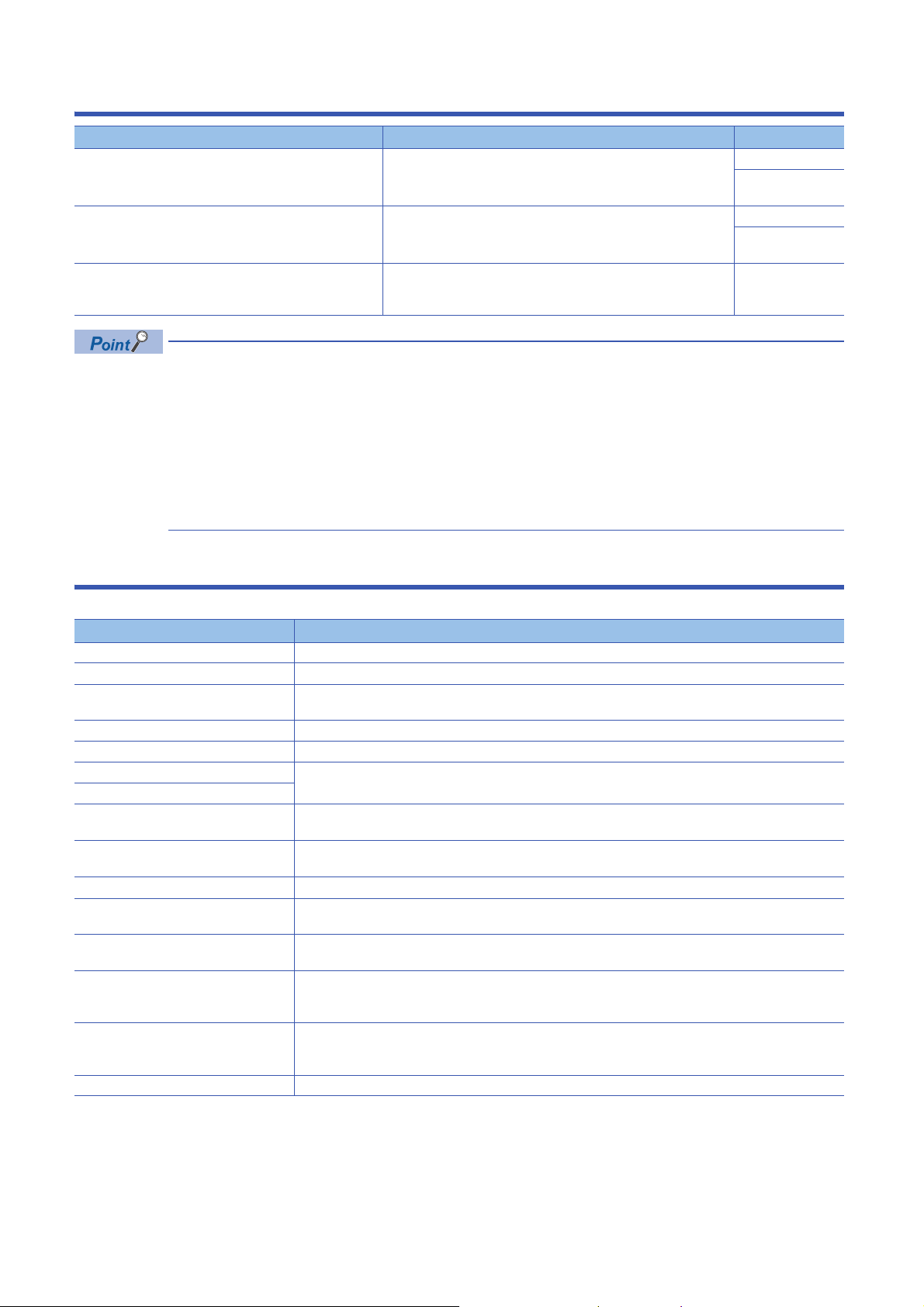
Mode transitions
At the power-on or at the
reset of the CPU module
(5)
(2)
(1)
(4)
(3)
Normal mode
Wave output mode
Offset/gain
setting mode
*1
The following figure and table describe the transition condition for each mode.
No. Transition condition
(1) Set "Operation mode setting" to "Normal mode (D/A conversion process)" in "Basic settig" of the engineering tool and set "Output mode
setting" to "Normal output mode".
(2) Set "Operation mode setting" to "Offset/gain setting mode” in "Basic settig" of the engineering tool.
(3) Perform the mode transition by either of the following methods.
Method 1 Execute the G(P).OFFGAN instruction (Argument "S": 0: Transition to the normal output mode).
Method 2 Set the following values for 'Mode switching setting' (Un\G296, Un\G297) and turn on and off 'Operating condition setting
request' (Y9).
• Un\G296: 5260H
• Un\G297: 4441H
(4) Perform the mode transition by either of the following methods.
Method 1 Execute the G(P).OFFGAN instruction (Argument "S": 1: Transition to the offset/gain setting mode).
Method 2 Set the following values for 'Mode switching setting' (Un\G296, Un\G297) and turn on and off 'Operating condition setting
request' (Y9).
• Un\G296: 4441H
• Un\G297: 5260H
(5) Set "Operation mode setting" to "Normal mode (D/A conversion process)" in "Basic settig" of the engineering tool and set "Output mode
setting" to "Wave output mode".
*1 The wave output mode is independent of the other modes. After the module is powered on in the wave output mode, the transition to the
other modes is disabled.
After the module is powered on in any mode other than the wave output mode, the transition to the wave output mode is also disabled.
1
Checking method
The currently selected mode can be checked with the following items.
Mode RUN LED status Stored value of 'Output mode'
Normal mode Normal output
Offset/gain setting mode Flashing 0 ON
*1 When 'User range write request' (YA) is off
'Offset/gain setting mode
(Un\G60)
mode
Wave output
mode
ON 0 OFF
ON 1 OFF
status flag' (XA)
*1
*1
1 FUNCTIONS
1.1 Modes
17
Page 20
1.2 Range Switching Function
The output range of the analog output can be switched for each channel.
Switching the range makes it possible to change the I/O conversion characteristic.
Setting procedure
Set the output range to be used in "Output range setting".
Navigation window [Parameter] [Module Information] Module name [Module parameter] "Basic settig"
"Range switching function"
Output range setting Digital input range
R60DA4 R60DAV8 R60DAI8
4 to 20mA 0 to 32000 0 to 32000
0 to 20mA
1 to 5V 0 to 32000 0 to 32000
0 to 5V
-10 to 10V -32000 to 32000 -32000 to 32000
User range (Voltage) -32000 to 32000 -32000 to 32000
User range (Current) -32000 to 32000 -32000 to 32000
After the data is written, the range is switched when the programmable power supply is turned off and on or when the CPU
module is reset.
The following buffer memory areas are used to monitor the range setting and to switch the range.
• 'CH1 Range setting' (Un\G598)
• 'CH1 Range setting monitor' (Un\G430)
For details on the buffer memory areas, refer to the following.
Page 164 CH1 Range setting
Page 145 CH1 Range setting monitor
Precautions
The output range cannot be changed for channels set to D/A conversion disabled. To change the output range, set "D/A
conversion enable/disable setting" to "D/A conversion enabled" and 'CH1 Output enable/disable flag' (Y1) to OFF.
18
1 FUNCTIONS
1.2 Range Switching Function
Page 21

1.3 D/A Conversion Enable/Disable Function
Set whether to enable or disable the D/A conversion for each channel.
Disabling the D/A conversion for unused channels reduces the D/A conversion cycles.
Setting procedure
Set "D/A conversion enable/disable setting" to "D/A conversion enable” or "D/A conversion disable".
Navigation window [Parameter] [Module Information] Module name [Module parameter] "Basic settig"
"D/A conversion enable/disable function"
1.4 D/A Output Enable/Disable Setting Function
Specify whether to output the D/A conversion value or offset value for each channel.
The conversion speed is a constant, regardless of the output enable/disable state.
Setting procedure
Set to enable or disable the D/A output for each channel with 'CH1 Output enable/disable flag' (Y1).
'CH1 Output enable/disable flag' (Y1) Analog output
Enable (ON) The D/A conversion value is output.
Disable (OFF) The offset value is output.
1
1 FUNCTIONS
1.3 D/A Conversion Enable/Disable Function
19
Page 22
1.5 Analog Output HOLD/CLEAR Function
Set whether to hold or clear the analog output value that has been output when the operating status of the CPU module is
RUN, STOP, or stop error.
The HOLD/CLEAR setting can be checked with 'CH1 HOLD/CLEAR function setting monitor' (Un\G431).
Operation
When the operating status of the CPU module is RUN, STOP, or stop error, the analog output status changes as shown in the
following table, depending on the combination of the settings of the analog output HOLD/CLEAR setting, 'CH1 D/A conversion
enable/disable setting' (Un\G500), and 'CH1 Output enable/disable flag' (Y1).
■In the normal output mode
Execution
status
Analog output produced when the CPU module
is in the RUN status
Analog output produced when the CPU module
is in the STOP state
Analog output produced when the CPU module
is in the stop error state
Analog output produced when a watchdog timer
*1
error
CH1 D/A conversion
enable/disable setting
(Un\G500)
CH1 Output enable/disable
flag (Y1)
Analog output HOLD/
CLEAR setting
occurs
Enable Disable
Enable Disable Enable or disable
HOLD CLEAR HOLD or CLEAR HOLD or CLEAR
The digital value converted in analog is output. Offset value 0V/0mA
Hold Offset value Offset value
Hold Offset value Offset value 0V/0mA
0V/0mA 0V/0mA 0V/0mA 0V/0mA
*2
0V/0mA
*1 The error occurs due to a hardware failure of the D/A converter module or other causes. 'Module READY' (X0) and the RUN LED of the
D/A converter module turn off.
When a watchdog timer error occurs, 'Module READY' (X0) and the RUN LED of the D/A converter module turn off.
*2 The following operation is performed when the CPU module is in the STOP state, the D/A conversion enable/disable setting is set to D/
A conversion enable (0) for the channel where HOLD is set, and 'Operating condition setting request' (Y9) is turned on and off.
When Output enable/disable flag is off: Outputs 0V/0mA.
When Output enable/disable flag is turned on: Outputs the offset value.
■In the wave output mode
Execution
status
Analog output produced when the CPU module is
in the RUN status
Analog output produced when the CPU module is
in the STOP state
Analog output produced when the CPU module is
in the stop error state
Analog output produced when a watchdog timer
*1
error
CH1 D/A conversion
Enable Disable
enable/disable setting
(Un\G500)
CH1 Output enable/disable
Enable Disable Enable or
flag (Y1)
Analog output HOLD/
HOLD CLEAR HOLD or
CLEAR setting
Wave output status Output Stop Pause Output Stop Pause
Wave
data
Hold Offset value Offset value 0V/0mA
Hold Offset value Offset value 0V/0mA
0V/0mA 0V/0mA 0V/0mA 0V/0mA
occurs
*2
Hold Wave
data
disable
HOLD or
CLEAR
*2
Offset
value
Offset value 0V/0mA
CLEAR
*1 The error occurs due to a hardware failure of the D/A converter module or other causes. 'Module READY' (X0) and the RUN LED of the
D/A converter module turn off.
When a watchdog timer error occurs, 'Module READY' (X0) and the RUN LED of the D/A converter module turn off.
*2 The output set in 'CH1 Output setting during wave output stop' (Un\G524).
1 FUNCTIONS
20
1.5 Analog Output HOLD/CLEAR Function
Page 23
■In the synchronization normal output mode
Execution
status
External
power
supply
READY flag
(X7): On
External power supply READY flag (X7): Off 0V/0mA 0V/0mA 0V/0mA 0V/0mA
Analog output produced when a watchdog timer
*1
error
*1 The error occurs due to a hardware failure of the D/A converter module or other causes. 'Module READY' (X0) and the RUN LED of the
D/A converter module turn off.
When a watchdog timer error occurs, 'Module READY' (X0) and the RUN LED of the D/A converter module turn off.
CH1 D/A conversion
enable/disable setting
(Un\G500)
CH1 Output enable/disable
flag (Y1)
Analog output HOLD/
CLEAR setting
Analog output produced when the
CPU module is in the RUN status
Analog output produced when the
CPU module is in the STOP state
Analog output produced when the
CPU module is in the stop error
state
occurs
Enable Disable
Enable Disable Enable or disable
HOLD CLEAR HOLD or CLEAR HOLD or CLEAR
CH1 Synchronization digital value (Un\G9500) Offset value 0V/0mA
Hold Offset value Offset value
Hold Offset value Offset value 0V/0mA
0V/0mA 0V/0mA 0V/0mA 0V/0mA
*2
0V/0mA
Setting procedure
Set "Analog output HOLD/CLEAR setting" to "HOLD" or "CLEAR".
Navigation window [Parameter] [Module Information] Module name [Module parameter] "Basic settig"
"Output mode setting function"
1
Precautions for when the remote head module has been mounted
When the D/A converter module has been mounted on the remote head module, set whether to hold or clear the analog
output value that has been output when the host station is disconnected with "CPU error output mode setting" of the module
parameter.
The following describes the settings required for using "CPU error output mode setting".
• Enable the station-based block data assurance for cyclic data on the sending side.
• To hold the analog output value, set "CPU error output mode setting" to "Hold". The analog output HOLD/CLEAR function
setting is disabled.
This setting is enabled for each module and cannot be set for each channel. To match the output status of when a stop error
occurs or the CPU module is in the STOP state and that of when the host station is disconnected, set "Analog output HOLD/
CLEAR setting" to the same value in all the channels.
Operating status CPU error output mode setting
The analog output value is held. Hold HOLD
The analog output value is cleared.
(The offset value is output.)
*1 "CPU error output mode setting" is enabled in the following cases.
When the host station is disconnected due to a network error
When the data link is stopped by the CC-Link IE Field Diagnostics of the engineering tool
Clear CLEAR
*1
Analog output HOLD/CLEAR setting
(Set the same value in all the channels.)
1 FUNCTIONS
1.5 Analog Output HOLD/CLEAR Function
21
Page 24
1.6 Analog Output Test when CPU Module is in STOP
RUN
Offset value
OFF
*1
OFF
ON
*2
ON
Offset value
RUNSTOP
D/A-converted value is output even when the CPU module is in STOP status.
Analog output value
converted from digital value
Analog output value
converted from digital value
Analog output value
converted from digital value
CH1 Output
enable/disable
flag (Y1)
Analog output
value status
CPU module
status
Controlled by the D/A converter module
Status Function
Analog output tests can be carried out when the CPU module is in the STOP status.
The following functions are enabled during the analog output test.
• Scaling function (Page 23 Scaling Function)
• Shift function (Page 26 Shift Function)
• Alert output function (Page 28 Alert Output Function)
When a digital value that is out of the setting range is written, a digital value setting range error (error code: 191H) occurs
and the corresponding check code is stored in 'CH1 Setting value check code' (Un\G400).
Operation
By forcibly turning on 'CH1 Output enable/disable flag' (Y1) when the CPU module is in the STOP state, the analog output
value is changed from the offset value to the D/A-converted analog output value.
The following figure shows the relation between 'CH1 Output enable/disable flag' (Y1) and the analog output value of the CPU
module in the STOP state when the analog output HOLD/CLEAR setting is set to CLEAR (0).
*1 'CH1 Output enable/disable flag' (Y1) turns off when the status of the CPU module is changed into STOP.
*2 By forcibly turning on 'CH1 Output enable/disable flag' (Y1), the analog output value is changed from the offset value to the D/A-
converted analog output value.
Setting procedure
To perform an analog output test, configure the settings in the device test of the engineering tool following the procedure
shown below.
1. Set 'CH1 D/A conversion enable/disable setting' (Un\G500) of the buffer memory to D/A conversion enabled (0).
2. Turn on 'Operating condition setting request' (Y9).
3. Check that 'Operating condition setting completed flag' (X9) turns off, and turn off 'Operating condition setting request'
(Y9).
4. Set the digital value equivalent to the analog value to be output for 'CH1 Digital value' (Un\G460) in the buffer memory.
5. Turn on 'CH1 Output enable/disable flag' (Y1).
22
1 FUNCTIONS
1.6 Analog Output Test when CPU Module is in STOP Status Function
Page 25

1.7 Scaling Function
× (DX - SL)
SH - S
L
32000
=
Digital value used for D/A
conversion
SH - S
L
64000
× (DX - SL) - 32000
Digital value used for D/A
conversion
=
× (DX - SL)
SH - S
L
32000
=
Digital value used for D/A
conversion
This function performs the scale conversion on digital values within a specified range between a scaling upper limit value and
a scaling lower limit value. The program for scale conversion can be omitted.
Operation
The scale conversion is performed for the set 'CH1 Digital value' (Un\G460) using 'CH1 Scaling upper limit value' (Un\G504)
and 'CH1 Scaling lower limit value' (Un\G506), and the value after the scale conversion is used for the D/A conversion. (In the
scale conversion, values after the decimal point are rounded off.)
When the relation between the set upper limit value and lower limit value is Scaling lower limit value > Scaling upper limit
value, the scale conversion can be performed according to a negative slope.
Concept of scaling setting
The necessary settings for the scaling lower limit value and scaling upper limit value depend on whether the factory default
setting or the user range setting is used for the analog output range.
■When the factory default setting is used for the analog output range
• For the scaling upper limit value, set a value corresponding to the upper limit value of the set analog output value.
• For the scaling lower limit value, set a value corresponding to the lower limit value of the set analog output value.
■When the user range setting is used for the analog output range
• Set a value corresponding to the gain value for the scaling upper limit value.
• Set a value corresponding to the offset value for the scaling lower limit value.
1
Calculating the scaling value
For D/A conversion, the scaling value is calculated based on the following equations.
■When the factory default setting is used for the output range
• When the voltage is 1 to 5V or 0 to 5V and the current is 4 to 20mA or 0 to 20mA
• When the voltage is -10 to 10V
■When the user range setting is used for the output range
Item Description
D
X
S
H
S
L
Digital value
Scaling upper limit value
Scaling lower limit value
1 FUNCTIONS
1.7 Scaling Function
23
Page 26
Setting procedure
Ex.
0
5
0
32000
Analog output voltage (V)
Scaling lower limit
value 4000
Scaling upper limit
value 14000
Digital value
1. Set "D/A conversion enable/disable setting" to "D/A conversion enable".
Navigation window [Parameter] [Module Information] Module name [Module parameter] "Basic settig"
"D/A conversion enable/disable function"
2. Set "Scaling enable/disable setting" to "Enable".
Navigation window [Parameter] [Module Information] Module name [Module parameter] "Application
setting" "Scaling setting"
3. Set values for "Scaling upper limit value" and "Scaling lower limit value".
Set the values to satisfy the following relation.
Scaling upper limit value Scaling lower limit value
Item Setting range
Scaling upper limit value -32000 to 32000
Scaling lower limit value
Example of scaling setting
When 14000 is set to the scaling upper limit value and 4000 is set to the scaling lower limit value for the channel with the
output range of 0 to 5V
Digital value Digital value after scaling Output voltage (V)
4000 0 0
6000 6400 1
8000 12800 2
10000 19200 3
12000 25600 4
14000 32000 5
24
1 FUNCTIONS
1.7 Scaling Function
Page 27

Precautions
• When the scaling function is used, the digital value can be set to a value out of the range between the scaling upper limit
value and scaling lower limit value (in the dotted lines in the I/O characteristics graph) before being scaled. However, use
the scaling function within the range of the analog output practical range (in the solid line in the I/O characteristics graph). If
the value exceeds the analog output practical range, the maximum resolution and accuracy may not fall within the range of
the performance specifications.
• The default digital value "0" may not be appropriate, depending on the scaling function setting.
In particular in the examples of when the output range is 0 to 5V, an out-of-range digital value error occurs if 'CH1 Output
enable/disable flag' (Y1) is turned on with the digital value "0".
A digital value setting range error (error code: 191H) occurs and 'Error flag' (XF) turns on, and the ERR LED lights.
Therefore, set an appropriate digital value within the scaling range before turning on 'CH1 Output enable/disable flag' (Y1).
• When using the user range, note that the scaling lower limit value is equal to the offset value.
• When the scaling function is enabled and the digital value after the scaling conversion is out of the digital setting range, a
digital value setting range error (error code: 191H) occurs and the corresponding check code is stored in 'CH1 Setting
value check code' (Un\G400).
• The scaling function is enabled only for the normal output. When the scaling function is enabled while the wave output
function is used, a scaling setting error in wave output mode (error code: 0B1H) occurs and 'Alert output signal' (XE) turns
on.
1
1 FUNCTIONS
1.7 Scaling Function
25
Page 28
1.8 Shift Function
Ex.
0
5
0
32000
31950
-50
Analog output voltage (V)
Input value
shift
After
adjustment
Before
adjustment
digital value
This function adds the set input value shift amount to the digital input value.
The analog output value reflects the change in the input value shift amount on a realtime basis. Therefore, fine adjustment
can be easily performed when the system starts.
Operation
When the D/A conversion is performed on the digital value, the value obtained by adding 'CH1 Input value shift amount'
(Un\G480) to 'CH1 Digital value' (Un\G460) is used for the D/A conversion.
When the digital value after the addition exceeds the range of -32768 to 32767 as the result of the shift processing, the value
is fixed with the lower limit value (-32768) or the upper limit value (32767).
When a value is written to 'CH1 Input value shift amount' (Un\G480), the set value is added to the digital input value
regardless of the ON/OFF state of 'Operating condition setting request' (Y9).
Setting procedure
Set the shift amount to "Input value shift amount".
Navigation window [Parameter] [Module Information] Module name [Module parameter] "Application
setting" "Shift function"
Item Setting range
Input value shift amount -32768 to 32767
Setting example
When the output range is 0 to 5V and the input value shift amount is +50
Digital value Analog output voltage (V)
Before adjustment After adjustment
-50 0 0
31950 32000 5
1 FUNCTIONS
1.8 Shift Function
26
Page 29

Precautions
• Based on the digital value on which the shift-and-add is performed, the alert output function, scaling function, and rate
control function are executed.
• When the value obtained by adding 'CH1 Input value shift amount' (Un\G480) to 'CH1 Digital value' (Un\G460) is out of the
digital setting range, a digital value setting range error (error code: 191H) occurs and the corresponding check code is
stored in 'CH1 Setting value check code' (Un\G400).
• The shift function is enabled only for the normal output. When a value other than 0 is set in 'CH1 Input value shift amount'
(Un\G480) while the wave output function is used, an input value shift amount setting error in wave output mode (alarm
code: 0B2H) occurs and 'Alert output signal' (XE) turns on. Although the wave output continues, 'CH1 Input value shift
amount' (Un\G480) is not added to the wave data to be output.
• Even though 0 is set for 'CH1 Input value shift amount' (Un\G480) after an input value shift amount setting error in wave
output mode has occurred, 'Alert output signal' (XE) does not turn off. Turn on and off 'Alert output clear request' (YE) to
turn off 'Alert output signal' (XE). By this operation, 'Alert output signal' (X8) and the ALM LED turn off, and Latest alarm
code is cleared.
1
1 FUNCTIONS
1.8 Shift Function
27
Page 30
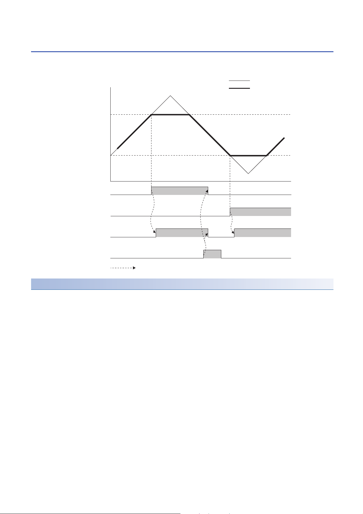
1.9 Alert Output Function
CH1 Alert output upper limit value
OFF ON
Alert output signal (XE)
OFF
OFF ON
CH1 Alert output lower limit value
20000
-2000
Digital value
Alert output upper flag
Alert output lower flag
Alert output clear request (YE)
OFF
Digital value
Analog output value
ON ON
ON OFF
OFF
OFF
Controlled by the D/A converter module
This function outputs an alert when the digital value is larger than the alert output upper limit value or is smaller than the alert
output lower limit value.
Operation
■Alert output notification
When 'CH1 Digital value' (Un\G460) is larger than 'CH1 Alert output upper limit value' (Un\G510) or is smaller than 'CH1 Alert
output lower limit value' (Un\G512), either of 'Alert output upper limit flag' (Un\G36) or 'Alert output lower limit flag' (Un\G37),
'Alert output signal' (XE), and the ALM LED turn on to output an alert. In addition, an alarm code (080H or 081H) is stored
in 'Latest alarm code' (Un\G2) when an alert has occurred.
When an alert has occurred, the set value of the alert output upper limit value or the alert output lower limit value is used as
the digital value for the D/A conversion.
When 'CH1 Digital value' (Un\G460) is changed to a value smaller than 'CH1 Alert output upper limit value' (Un\G510) and
larger than 'CH1 Alert output lower limit value' (Un\G512) after an alert has occurred, the analog output value returns to a
normal value. However, 'Alert output upper limit flag' (Un\G36), 'Alert output lower limit flag' (Un\G37), and 'Alert output signal'
(XE) are not cleared.
28
1 FUNCTIONS
1.9 Alert Output Function
Page 31

Clearing a warning
The alert output can be cleared in the following two methods:
After 'CH1 Digital value' (Un\G460) is set to be smaller than 'CH1 Alert output upper limit value' (Un\G510) and larger than
'CH1 Alert output lower limit value' (Un\G512)
• Turning on and off 'Alert output clear request' (YE)
• Turning on and off 'Operating condition setting request' (Y9)
The D/A converter module arranges the following status when an alert output is cleared.
• Clearing 'Alert output upper limit flag' (Un\G36) and 'Alert output lower limit flag' (Un\G37)
• Turning off 'Alert output signal' (XE)
• Turning off the ALM LED
• Clearing the alarm code stored in 'Latest alarm code' (Un\G2)
Setting procedure
1. Set "Alert output setting" to "Enable".
Navigation window [Parameter] [Module Information] Module name [Module parameter] "Application
setting" "Alert output function"
2. Set values for "Alert output upper limit value" and "Alert output lower limit value".
Set the values to satisfy the following relation.
Alert output upper limit value > Alert output lower limit value
Item Setting range
Alert output upper limit value -32768 to 32767
Alert output lower limit value
1
Precautions
• When the shift function is used in the normal mode, 'CH1 Digital value' (Un\G460) on which the shift-and-add is performed
is the alert detection target. Set the alert output upper/lower limit values in consideration of the shift-and-add.
1 FUNCTIONS
1.9 Alert Output Function
29
Page 32

1.10 Rate Control Function
The increment/decrement of the analog output value per 80s is restricted to prevent the sudden change of the analog output
value.
When the inter-module synchronization function is enabled, the rate control function cannot be used.
Operation
When the change amount of 'CH1 Digital value' (Un\G460) is larger than the value set in 'CH1 Increase digital limit value'
(Un\G514) or 'CH1 Decrease digital limit value' (Un\G516), this function changes 'CH1 Digital value' (Un\G460) by the limit
values set for each digital limit value.
The increment/decrement values per 80s are set for 'CH1 Increase digital limit value' (Un\G514) and 'CH1 Decrease digital
limit value' (Un\G516). However, the actual update cycle of the output value of the corresponding channel is (80s Number
of conversion-enabled channels).
Therefore, the analog output value increases or decreases per update cycle as follows:
First time: The D/A conversion value of the increase/decrease digital limit value
Second time or later: The D/A conversion value of (Increase/decrease digital limit value Number of conversion-enabled
channels)
Setting procedure
1. Set "Rate control enable/disable setting" to "Enable".
Navigation window [Parameter] [Module Information] Module name [Module parameter] "Application
setting" "Rate control function"
2. Set values for "Increase digital limit value" and "Decrease digital limit value".
Item Setting range
Increase digital limit value 0 to 64000
Decrease digital limit value
30
1 FUNCTIONS
1.10 Rate Control Function
Page 33

Operation example of the rate control function
<CH1>
1.25V
V
t
2.50V
1.25V
V
t
2.50V
1.25V
V
t
2.50V
4400
4200
4600 6400 80004000
5600 6800 8000
4800 5400 6000 6600 7200 7800 8000
4000 (1.25V) 8000 (2.5V)
600
4000 (1.25V) 8000 (2.5V)
4000 (1.25V) 8000 (2.5V)
400
200
123123123123123123121231231232 3
<CH2>
<CH3>
+600 +1800 +1600
+400 +1200 +1200 +1200
+600+200 +200+600 +600 +600 +600 +600
4000
4000
(Buffer memory)
analog output
Change in the digital
value of internal
CH1 Digital value
CH1 Increase digital limit value
CH2 Digital value
CH3 Digital value
CH2 Increase digital limit value
CH3 Increase digital limit value
Conversion speed = 80µs
Change in the digital
value of internal
Change in the digital
value of internal
Difference
between
the change
Difference
between
the change
Difference
between
the change
Conversion channel
Refresh cycle of output value = 240µs
The following figure shows an operation example when CH1 Rate control enable/disable setting to CH3 Rate control enable/
disable setting are set to Enable (0) and each increase digital limit value is set to 600, 400, and 200.
1
1 FUNCTIONS
1.10 Rate Control Function
31
Page 34

Precautions
RUN
STOP
RUN
Analog output value
The digital input value
converted in analog
Offset value
Rate control enabled
The digital input value
converted in analog
CPU module status
(error)
RUN
STOP
RUN
Analog output value
The digital input value
converted in analog
Offset value
Rate control enabled
The digital input value
converted in analog
CPU module status
(error)
• The setting of the shift function is enabled during the rate control.
• When the alert output function is enabled, the alert determination is performed to the set 'CH1 Digital value' (Un\G460).
Note that an alert does not occur at the timing when the digital value changed by the rate control function exceeds the
upper/lower limit value.
• The rate control does not function during the analog output test for when the CPU module is in the STOP state.
• With Analog output HOLD/CLEAR setting set to a value other than HOLD, the analog output value changes when the CPU
module is in the STOP state but the rate control function does not function.
• When the CPU module status changes while the D/A conversion and D/A output are enabled and the analog output HOLD/
CLEAR setting is set to CLEAR, the rate control function operates as follows:
When the CPU module status changes from RUN to STOP (error), the rate control does not function. When the CPU
module status changes from STOP (error) to RUN, the rate control functions.
• When the CPU module status is changed from STOP (error) to RUN while the D/A conversion is enabled, the D/A output is
enabled, analog output is set to HOLD, and the rate control is enabled, the analog output is restarted from the offset value.
• When the D/A conversion is enabled and the D/A output is disabled, the rate control does not function.
• When a value out of the setting range is written to 'CH1 Digital value' (Un\G460) during the rate control, the rate control is
performed with the upper or lower limit value of the setting range.
In addition, the check result is stored in 'CH1 Setting value check code' (Un\G400).
• When the external power supply is turned off during the rate control, the rate control does not function and the analog
output value changes to 0V/0mA. When the external power supply is recovered, the rate control is restarted from the offset
value.
• The rate control function is enabled only for the normal output. When the rate control function is enabled while the wave
output function is used, a rate control setting error in wave output mode (alarm code: 0B3H) occurs and 'Alert output
signal' (XE) turns on.
32
1 FUNCTIONS
1.10 Rate Control Function
Page 35

1.11 External Power Supply Disconnection Detection
Function
This function detects that the external power supply 24VDC is not supplied or the supply stops.
When the external power supply disconnection is detected, 'External power supply READY flag' (X7) turns off, and the analog
output value becomes 0V/0mA regardless of the other settings.
Operation
When the external power supply is not input or when 200ms has not yet elapsed after the power supply is input, the power
supply is regarded as disconnected and 'External power supply READY flag' (X7) turns off.
When the external power supply input stops, the external power supply is regarded as disconnected and 'External power
supply READY flag' (X7) turns off.
Precautions
When the external power supply does not satisfy the requirements of the performance specifications, the external power
supply is regarded as disconnected.
For the performance specifications of the external power supply, refer to the following.
MELSEC iQ-R Digital-Analog Converter Module User's Manual (Startup)
1
1 FUNCTIONS
1.11 External Power Supply Disconnection Detection Function
33
Page 36

1.12 Disconnection Detection Function
ON
ON
ON
OFF
OFF
OFF
0mA
OFF
OFF
OFF
Analog output value
Time
Disconnection detection
signal (XD)
Disconnection detection
flag (Un\G38.b0)
Error clear request (YF)
Resume output
Disconnection
detection
Controlled by the D/A converter module
Controlled by the program
Threshold of
disconnection detection
Within the detection range
Outside the detection range
Included
CH1 Analog
output value
Was removed and
the disconnection
cause
The R60DA4 and R60DAI8 can detect a disconnection by monitoring the analog output value. This function is enabled only
when the analog output range is 4 to 20mA. A disconnection can be detected for each channel.
Operation
■Disconnection detection
A disconnection can be detected when the analog output range is 4 to 20mA and 'CH1 D/A conversion enable/disable setting'
(Un\G500) is set to D/A conversion enabled (0).
■Operations performed when a disconnection is detected
When a disconnection is detected, the disconnection is notified by turning on 'Disconnection detection flag' (Un\G38),
'Disconnection detection signal' (XD), and the ERR LED.
In addition, an error code (1C4H) is stored in 'Latest error code' (Un\G0).
Even if the disconnection cause is eliminated, the analog output does not restart automatically to prevent an incorrect output.
To restart the analog output, check 'CH1 Digital value' (Un\G460) and turn on and off 'Error clear request' (YF). According to
the status of 'CH1 Output enable/disable flag' (Y1), the analog output restarts.
When the analog output restarts, 'Disconnection detection flag' (Un\G38) of the corresponding channel is cleared. When the
analog output of all the channels restarts, 'Disconnection detection signal' (XD) is cleared.
34
1 FUNCTIONS
1.12 Disconnection Detection Function
Page 37

1.13 Interrupt Function
The D/A converter module executes the interrupt program of the CPU module when an interrupt factor such as a
disconnection or alert output is detected.
For the D/A converter module, the maximum number of interrupt pointers available is 16 per module.
Operation
■Detecting an interrupt factor
When an interrupt factor occurs, an interrupt request is sent to the CPU module at the same time as 'Interrupt factor detection
flag [n]' (Un\G4 to Un\G19) is turned to Interrupt factor (1).
■How to reset an interrupt factor
When Reset request (1) is set to 'Interrupt factor reset request [n]' (Un\G156 to Un\G171) corresponding to the interrupt factor,
the specified interrupt factor is reset and 'Interrupt factor detection flag [n]' (Un\G4 to Un\G19) changes to No interrupt factor
(0).
Setting procedure
To use the interrupt function, set "Condition target setting", "Condition target channel setting", "Interrupt factor transaction
setting", and "Interrupt pointer" in the engineering tool. After completing the settings, write the project to enable the settings.
Navigation window [Parameter] [Module Information] Module name [Module parameter] "Interrupt setting"
The following table shows the setting items on the interrupt setting window.
Item Description
Condition target setting Select a factor of the target for the interrupt detection.
Condition target channel setting Select a target channel when the condition target setting for the interrupt
detection is channel specification.
Interrupt factor transaction setting Set an interrupt request for when the same interrupt factor occurs during the
interrupt factor detection.
Interrupt pointer Specify the number of an interrupt pointer that is initiated at the detection of an
interrupt factor.
1
■Condition target setting
Select a factor of the condition target setting for the interrupt detection.
For details on the factors to be detected, refer to the following.
Page 142 Condition target setting [n]
■Condition target channel setting
Select a target channel when the condition target setting for the interrupt detection is channel specification.
Item Setting value
Condition target channel
setting
*1 When X signal is specified for the condition target setting, this value is ignored.
0: All channels 1: CH1 2: CH2 3: CH3 4: CH4 5: CH5 6: CH6 7: CH7 8: CH8
*1
■Interrupt factor generation setting
Set an interrupt request for when the same interrupt factor occurs during the interrupt factor detection.
• When Interrupt resend request (0) is set and the same interrupt factor occurs during the interrupt factor detection, an
interrupt request is sent to the CPU module again.
• When No interrupt resend request (1) is set and the same interrupt factor occurs during the interrupt factor detection, an
interrupt request is not sent to the CPU module.
■Interrupt pointer
To the interrupt pointer, specify a number of an interrupt pointer to be activated when an interrupt factor is detected or the
label related to the interrupt pointer. For details on the interrupt pointers, refer to the following.
MELSEC iQ-R CPU Module User's Manual (Application)
1 FUNCTIONS
1.13 Interrupt Function
35
Page 38

• If 'Condition target setting [n]' (Un\G232 to Un\G247) is Disable (0), an interrupt request is not sent to the
CPU module.
• To reset the interrupt factor, set Reset request (1) until 'Interrupt factor detection flag [n]' (Un\G4 to Un\G19)
changes to No interrupt factor (0).
• Resetting interrupt factors is executed only when 'Interrupt factor reset request [n]' (Un\G156 to Un\G171)
changes from No reset request (0) to Reset request (1).
• Multiple interrupt pointers can also share the same setting of 'Condition target setting [n]' (Un\G232 to
Un\G247). When interrupts with the same settings occur in 'Condition target setting [n]' (Un\G232 to
Un\G247), the interrupt program is executed in order of the priority of the interrupt pointers. For the priority
of the interrupt pointers, refer to the following.
MELSEC iQ-R CPU Module User's Manual (Application)
• When All channels (0) is set for 'Condition target channel setting [n]' (Un\G264 to Un\G279) and an interrupt
detection target for each channel is set to 'Condition target setting [n]' (Un\G232 to Un\G247) such as Alert
output flag (2), the interrupt requests that have the same interrupt factor are sent to the CPU module if alerts
are issued in multiple channels. In this case, the CPU module executes multiple interrupt programs at a time
and judges that the program cannot be normally finished due to the scan monitoring function of the CPU
module, and a CPU module error may occur. When a CPU error occurs, refer to the following.
MELSEC iQ-R CPU Module User's Manual (Application)
36
1 FUNCTIONS
1.13 Interrupt Function
Page 39

Setting example
Ex.
When the interrupt program (I50) is executed at the disconnection detection in any channel
• Parameter setting
Set "Interrupt setting" of [Module parameter] as follows.
No. Condition target setting Condition target channel
setting
1 Disconnection detection flag All CH specification I50
• Label setting
Classification Label name Description Device
Module label RCPU.stSM.bAlways_ON Always ON SM400
RCPU.stSM.bAfter_RUN1_Scan_ON ON for one scan after RUN SM402
R60DA_1.unInterruptFactorMask_D[0].0 Interrupt factor mask [1] U0\G124.0
R60DA_1.unInterruptFactorResetRequest_D[0].0 Interrupt factor reset request [1] U0\G156.0
Labels to be defined Define global labels as shown below:
Interrupt pointer
1
(18) Enable only the interrupt pointer I50.
Enable the interruption.
Clear Interrupt factor mask [1].
(83) Turn on Interrupt factor reset request [1].
Perform the processing of when a disconnection is detected.
1 FUNCTIONS
1.13 Interrupt Function
37
Page 40

1.14 Wave Output Function
(2) Save the wave data to a CSV file or file register.
Save a CSV file in a SD memory card.
(3) Register the wave data to the wave data registry area in the
D/A converter module using a function block (FB) for wave data registration.
Subject to be controlled
Analog output
(4) Digital values are converted to
analog values in the set conversion
cycle, and the converted values are
output sequentially.
(1) Create wave data.
Wave data can be created with easy
mouse operation from "Create Wave
Output Data" of engineering tool.
D/A converter
module
Wave data
Wave data registry area
This function registers the prepared wave data (digital input value) in the D/A converter module and continuously outputs the
data (analog value) in the set conversion cycle. A faster and smoother control than a program is achieved by the automatic
output of the control wave data registered in the D/A converter module for the analog (torque) control such as pressing
machines and injection molding units. The control can be executed only by registering the wave data to the D/A converter
module. Therefore, the program-less control is available for the repeat control such as the line control, and man-hours for
programming can be reduced.
The wave output function can be used only when "Output mode setting" is set to "Wave output mode" of the basic setting.
This section calls the following items to be set for the wave output function as wave output data.
• Wave data (Page 46 Creating wave data)
• Parameters of the wave output function (Page 49 Setting parameters of the wave output function)
38
1 FUNCTIONS
1.14 Wave Output Function
Page 41

Wave output function procedure
The following shows how to use the wave output function.
1. Creating wave data
Page 46 Creating wave data
2. Setting parameters of the wave output function
Page 49 Setting parameters of the wave output function
3. Writing wave output data to a file register (ZR) or CSV file
Page 50 Writing data to a file register (ZR) or CSV file
4. Parameter setting of the D/A converter module
Page 51 Parameter setting of the D/A converter module
5. Registering wave output data
Page 52 Registering wave output data
6. Starting/stopping/pausing wave output
Page 54 Starting/stopping/pausing wave output
Wave output data can be easily created by using "Create Wave Output Data" of the engineering tool. These contents are
written to the file registers (ZR) of the CPU module or CSV files.
Parameter settings for the wave output function
To use the wave output function, the parameters of the wave output function are required to be set on the "Create Wave
Output Data" window.
Setting item Reference
Output setting during wave output stop Page 49 Setting parameters of the wave output function
Output value during wave output stop
Wave pattern start address setting
Wave pattern data points setting
Wave pattern output repetition setting
Constant for wave output conversion cycle
Wave data registry area
1
For details on each buffer memory area, refer to the following.
Page 136 Details of buffer memory addresses
1 FUNCTIONS
1.14 Wave Output Function
39
Page 42

Restrictions and precautions on the wave output function
The wave output function has the following restrictions and precautions.
■Output range setting
The user range cannot be used. When executing the wave output function, use the range other than the user range.
For the setting procedure of the output range, refer to the following.
Page 18 Range Switching Function
■Scaling function
The scaling function cannot be used when the wave output function is selected. When executing the wave output function,
disable the scaling function.
■Analog output HOLD/CLEAR function
The operation of the analog output HOLD/CLEAR function for the normal output differs from the operation for the wave output.
For details, refer to the following.
Page 20 In the wave output mode
■Remote head module
When the D/A converter module is mounted together with the remote head module, function blocks (FBs) cannot be used. To
execute the wave output function, refer to the following.
Page 58 Registering data when the remote head module is used
Wave data
The wave data indicate the time-series arrangement of the digital input values to be output in analog. Up to 80000 points can
be used. The wave data is registered in 'Wave data registry area' (Un\G10000 to Un\G89999).
40
1 FUNCTIONS
1.14 Wave Output Function
Page 43

Wave pattern
Ex.
Empty
(62000 points)
80000 points
8000 points10000 points
CH1
Wave pattern
CH2
Wave pattern
Wave data registry area
(Un\G10000 to Un\G89999)
Wave data registry area
(Un\G10000)
Wave data registry area
(Un\G89999)
To use the wave output function, select any points from the registered wave data for each channel and set the wave pattern.
The following table lists the setting contents for the wave pattern.
Setting item Description
Wave pattern start address setting Set the start address of the wave pattern to be output for each channel. The D/A conversion starts from the digital
input value of the buffer memory address set in this area and the converted values are output sequentially.
Wave pattern data points setting This area is for setting the points of the wave pattern to be output for each channel. From the start address of the
wave pattern, the D/A conversion starts for the points of wave data set in this area and the converted values are
output.
If the address value (total of the set values for "Wave pattern start address setting" and "Wave pattern data points setting" - 1)
exceeds the last buffer memory address (Un\G89999) of the wave data registry area, an error occurs. The error code
(1D9H) is stored in 'Latest error code' (Un\G0), 'Error flag' (XF) turns on, and the ERR LED turns on.
Setting example to output different waves from CH1 and CH2
1
Setting item Setting value
CH1 Wave pattern start address setting 10000
CH1 Wave pattern data points setting 10000
CH2 Wave pattern start address setting 20000
CH2 Wave pattern data points setting 8000
1 FUNCTIONS
1.14 Wave Output Function
41
Page 44

Ex.
Setting example to output the same waves from CH1 and CH2
Ex.
80000 points
CH1, CH2
Wave pattern
Wave data registry area
(Un\G10000 to Un\G89999)
Wave data registry area
(Un\G10000)
Wave data registry area
(Un\G89999)
The wave pattern is
output 3 times repeatedly.
Analog output
Wave pattern
1st time 2nd time 3rd time
After the wave pattern is output 3 times, wave output stops and
an analog value is output according to the setting in
CH1 Output setting during wave output stop (UnG\524).
Setting item Setting value
CH1 Wave pattern start address setting 10000
CH1 Wave pattern data points setting 80000
CH2 Wave pattern start address setting 10000
CH2 Wave pattern data points setting 80000
Wave pattern output count
The wave pattern can be output repeatedly according to the setting of 'CH1 Wave pattern output repetition setting' (Un\G530).
Set the output count within 1 to 32767. The wave pattern also can be output in analog repeatedly and unlimitedly when -1 is
set for the output count.
When the wave pattern output count is set to three
The following describes the repeat control in which the same wave pattern is output repeatedly from the D/A converter
module.
■When the digital input values are same for the start point and the end point
An end point of a wave pattern overlaps with the start point of the wave pattern of the next iteration in the D/A converter
module's processing; therefore, the end point is not output in analog. The analog output of the wave pattern end point varies
as follows depending on the setting of 'CH1 Wave pattern output repetition setting' (Un\G530).
• Limited repetition
When a value of 2 to 32767 is set to 'CH1 Wave pattern output repetition setting' (Un\G530), the digital input value of the end
point is not output in analog till the wave pattern of the final iteration output. After the digital input value of the end point is
output in analog at the wave pattern of the final iteration output, the value is output in analog according to the setting in 'CH1
Output setting during wave output stop' (Un\G524).
42
1 FUNCTIONS
1.14 Wave Output Function
Page 45

• Unlimited repetition
Ex.
Wave can be combined seamlessly by not outputting end point
data because the end point data overlaps with the start point
data of the next iteration.
A wave pattern that is repeatedly
output in an analog value
The digital values are
same for the start point
and the end point
*1
For the case where the wave pattern is repeatedly
output a limited number of times, the wave pattern
is output a number of times specified in Wave
pattern output repetition setting, and then the value
is output according to the setting in Output setting
during wave output stop.
Analog output
1 cycle
*1
1 cycle
1 cycle
1 cycle
Output cycle of
a wave pattern ( s)
Conversion
speed
=
Number of channels
where D/A conversion
is enabled
Constant for
wave output
conversion cycle
(Wave pattern
data points - 1)
80
=11100
8000
=
×
×
×
×
×
×
The digital input value of the wave pattern end point is not output in analog.
*1 The output cycle of a wave pattern is calculated by the following formula.
Output cycle of a wave pattern = (Wave output conversion cycle) (Wave pattern data points - 1)
For details on the wave output conversion cycle, refer to the following.
Page 45 Wave output conversion cycle
1
Calculating the output cycle of a wave pattern
Setting item Setting value
CH1 D/A conversion enable/disable setting D/A conversion enabled (0)
CH1 Wave pattern data points setting 101
CH1 Wave pattern output repetition setting 3
CH1 Constant for wave output conversion cycle 1
With the above setting, the output cycle of a wave pattern becomes as follows. (When the D/A conversion is enabled only for
CH1)
1 FUNCTIONS
1.14 Wave Output Function
43
Page 46

■When the digital input values are different between the start point and the end point
Ex.
The digital input values of the end point
and the start point of the next iteration
are consecutively output in an analog value.
A wave pattern that is repeatedly
output in an analog value
The digital input values are
different between the start
point and the end point.
*1
For the case where the wave pattern is repeatedly output
a limited number of times, the wave pattern is output a
number of times specified in Wave pattern output
repetition setting, and then the value is output according
to the setting in Output setting during wave output stop.
Analog output
1 cycle
*1
1 cycle 1 cycle
Conversion
speed
=
Number of channels
where D/A conversion
is enabled
Constant for
wave output
conversion cycle
Wave pattern
data points
80
=11101
8080
=
Output cycle of
a wave pattern ( s)
×××
×
×
×
The wave pattern end point is output in analog as it is. The set wave patterns are continuously output in analog regardless of
the setting in 'CH1 Wave pattern output repetition setting' (Un\G530).
*1 The output cycle of a wave pattern is calculated by the following formula.
Output cycle of a wave pattern = (Wave output conversion cycle) (Wave pattern data points)
For details on the wave output conversion cycle, refer to the following.
Page 45 Wave output conversion cycle
Calculating the output cycle of a wave pattern
Setting item Setting value
CH1 D/A conversion enable/disable setting D/A conversion enabled (0)
CH1 Wave pattern data points setting 101
CH1 Wave pattern output repetition setting 3
CH1 Constant for wave output conversion cycle 1
With the above setting, the output cycle of a wave pattern becomes as follows. (When the D/A conversion is enabled only for
CH1)
44
1 FUNCTIONS
1.14 Wave Output Function
Page 47

Wave output conversion cycle
Ex.
Conversion cycle ( s)
Conversion speed
(80 s)
=
Number of channels where
D/A conversion is enabled
Constant for wave output
conversion cycle
××
Wave output start
CH2: 640µs
CH3: 960µs
CH4: 1280µs
CH1: 320µs
320µs
80µs
640µs 640µs 640µs 640µs
320µs 320µs 320µs 320µs 320µs 320µs 320µs 320µs
960µs
1280µs 1280µs
960µs 960µs
The wave output conversion cycle is calculated by the following formula.
In the wave output function, the conversion cycle can be set by setting 'CH1 Constant for wave output conversion cycle'
(Un\G531). The conversion cycle of the current output wave can be checked in 'CH1 Wave output conversion cycle monitor'
(Un\G432, 433).
The conversion cycle and operation timing
Setting item Setting value
D/A conversion enable/disable setting D/A conversion enabled (0) for CH1 to CH4
CH1 Constant for wave output conversion cycle 1
CH2 Constant for wave output conversion cycle 2
CH3 Constant for wave output conversion cycle 3
CH4 Constant for wave output conversion cycle 4
The following figure shows the conversion cycle of each channel with the above settings.
• CH1: 320s
• CH2: 640s
• CH3: 960s
• CH4: 1280s
D/A conversion is performed with this conversion cycle, and an analog value is output.
1
1 FUNCTIONS
1.14 Wave Output Function
45
Page 48

Initial settings of the wave output function
Created end point
For the wave output function, set the following items as the initial setting. Before using the wave output function, complete the
procedures described in this section.
• Creating wave data (Page 46 Creating wave data)
• Setting parameters of the wave output function (Page 49 Setting parameters of the wave output function)
• Writing wave output data to a file register (ZR) or CSV file (Page 50 Writing data to a file register (ZR) or CSV file)
• Parameter setting of the D/A converter module (Page 51 Parameter setting of the D/A converter module)
This section uses the R60DA4 for explanation.
Creating wave data
Create wave data on the "Create Wave Output Data" window of the engineering tool.
1. Start "Create Wave Output Data".
[Tool] [Module Tool List] [Analog Output] [Create wave output data]
2. Select "Module Type" in "R60DA4".
If a type other than "Module Type" is selected, proper wave data cannot be created because the
corresponding channel or the range of digital values differs.
In addition, "Wave pattern" and "Wave output data" are completely deleted by changing "Module Type".
Therefore, set the correct value in "Module Type" and follow the procedure 3 or later.
3. Select the graph displayed in "Register wave pattern" and press the [Enter] key. The "Register Wave Pattern" window is
displayed.
4. Set "Wave pattern information".".
Item Description Setting range
Wave pattern No. The wave pattern number selected in the "Create Wave Output Data" window
is displayed. Up to 10 wave patterns can be created.
Wave pattern name Set the name of the wave pattern. 16 characters
Digital value range Select the setting range of the digital value according to the output range to be
used.
Number of data Set the number of the digital values of the wave pattern. 1 to 80000 (default value: 100)
Comment Set the comment of the wave pattern. 64 characters
• 0 to 32000 (default value)
• -32000 to 32000
5. Click any position on the wave graph to create an end point. The created end point is displayed with .
46
1 FUNCTIONS
1.14 Wave Output Function
Page 49

To delete the end point, move the mouse pointer to the point. Then select "Delete end point" from the right-click menu. When
Deleted end point
Start point
End point
Set "Direction".
In an upward direction In a downward direction
The arc to be drawn
1) Construct an equilateral triangle having the start
and end points as its vertices.
2) Construct a circle having the other vertex of the triangle
as its center and a side of the triangle as its radius.
3) Draw the minor arc connecting the start and
end points on the wave graph.
* The steps 1) and 2) are processed inside engineering tool,
and not displayed on the wave graph.
the mouse pointer is on the end point, the display of the mouse pointer is changed to .
6. Set the wave between end points from the right-click menu or in "Specify wave" of "Wave details setting".
Item Setting result
Circular arc The interval of the start point and end point is drawn in an arc. When the circular arc is selected, the arc direction can be set in "Direction"; it
can be inverted. The arc is drawn in the procedure below.
1
Straight line The interval of the start point and end point is drawn in a straight line.
Exponential
function
The graph is drawn with an adjustment so that the start point and end point are on the edge points of the exponential function of y = e
to 10).
1 FUNCTIONS
1.14 Wave Output Function
x
(X = 0
47
Page 50

Item Setting result
Drag
Logarithmic
function
Sine function
The graph is drawn with an adjustment so that the start point and end point are on the edge points of the logarithmic function of y = logeX (X
= 1 to 101).
*1
The interval between the start point and end point is drawn in a sine function wave. The amplitude A of the sine function to be drawn is the
value set in "Amplitude". The start position can be changed by 180 by setting "Phase".
Wx
Xed-Xst
Number of data in a wave pattern: Wx
Digital value range: Wy
Data position of the start point: Xst
Data position of the end point: Xed
A
Wy
Start point
Cosine
function
The interval between the start point and end point is drawn in a cosine function wave. The amplitude A of the cosine function to be drawn is
*1
the value set in "Amplitude". The start position can be changed by 180 by setting "Phase".
Wx
Start point
Xed-Xst
Number of data in a wave pattern: Wx
Digital value range: Wy
Data position of the start point: Xst
Data position of the end point: Xed
Wy
A
*1 When using the sine function and cosine function, set the same digital value for the start point and end point.
7. Drag the created end point to adjust the position.
End point
End point
The end point position also can be adjusted by changing the value of "End point" and "Digital value" in "Wave details setting".
Item Description
Start point The end point of the previous interval is displayed. To change the start point, change the end point of the previous interval.
End point Set the number of data (position) for the destination end point. Note that the section No.1 cannot be changed because it is the first
Digital value Set the digital value for the destination end point.
1 FUNCTIONS
48
1.14 Wave Output Function
point of the wave pattern.
Page 51

8. Repeat procedures 5 to 7 to create the wave to be output.
Each digital value of the created wave pattern can be checked by clicking the [Display Digital Value] button. Click the [Initialize
Graph] button to clear the contents in the created wave pattern. The graph and the contents of "Wave details setting" are
cleared.
9. Click the [Save Wave Patern] button.
The saved wave pattern can be opened by clicking the [Open Wave Patern] button.
10. Set the save destination and the file name, then click the [Save] button.
11. Click the [OK] button in the "Register Wave Pattern" window to register the created wave pattern.
12. Repeat procedures 3 to 12 to create other wave patterns.
Setting parameters of the wave output function
Set the parameters of the wave output function in the "Create Wave Output Data" window of the engineering tool. Before the
parameter setting, create the wave data.
1. Start "Create Wave Output Data".
[Tool] [Module Tool List] [Analog Output] [Create wave output data]
2. Select "Module Type" in "R60DA4".
3. Set the parameters of the wave output function in "Wave output data setting".
Item Description Setting range
Wave pattern No. Up to three patterns can be specified at a time from registered wave patterns. When
Output setting during wave
output stop
Output value during wav e output
stop
Wave pattern start address
setting
Wave pattern data points setting This setting is not required because the data points of the wave pattern to be used are
Wave pattern output repetition
setting
Constant for wave output
conversion cycle
specifying multiple wave patterns, set the pattern No. as follows.
• When No. 1 to No. 2 are used: 1 and 2
• When No. 1, No. 5, and No. 10 are used: 1, 5, and 10
• When No. 1 to No. 3 are used: 1 to 3
Set the analog output during the wave output stop. • 0: 0V/0mA
Set the value to be output while the wave output is stopped. This setting is enabled only
when "Output setting during wave output stop" is set to "2: Setting value during stop".
Set the value within the output range to be used.
Set the start address of the wave pattern to be output in analog. 10000 to 89999
stored automatically.
This area is for setting the repeat count to output the wave pattern repeatedly. • -1 (Unlimitedly repeat output)
Set the constant to determine the conversion cycle (specifying a multiple of the
conversion speed). The conversion cycle of the wave output is determined from the
combination of the conversion speed, number of channels where D/A conversion is
enabled, and this setting.
For the calculation method of the wave output conversion cycle, refer to the following.
Page 45 Wave output conversion cycle
1 to 10
• 1: Offset value (default value)
• 2: Output value during wave
output stop
• 4 to 20mA, 0 to 20mA, 1 to 5V,
0 to 5V: 0 to 32767 (practical
range: 0 to 32000)
• -10 to 10V: -32768 to 32767
(practical range: -32000 to
32000)
(default value: 10000)
• 1 to 32767 (default value: 1)
1 to 5000 (default value: 1)
1
4. Click the [Save Wave Output Data to File] button.
The created wave pattern and the parameter setting of the wave output function are saved.
The saved wave pattern and parameter setting of the wave output function can be opened by clicking the [Open Wave Output
Data from File] button.
Note that if the data created for the module type other than "R60DA4" is opened, the module type cannot be changed by
setting "Module type" to "R60DA4".
5. Set the save destination and the file name, then click the [Save] button.
1 FUNCTIONS
1.14 Wave Output Function
49
Page 52

Writing data to a file register (ZR) or CSV file
Write the wave output data created using "Create wave output data" to a file register (ZR)*1 or a CSV file *2.
These setting contents are registered to the buffer memory of the D/A converter module using the function block (FB) for the
wave output data registration.
For details on the function block (FB) for the wave output data registration and wave output execution, refer to the following.
MELSEC iQ-R Analog-Digital Converter Module/Digital-Analog Converter Module Function Block Reference
*1 The wave data and parameter setting contents remain in the CPU module even after the power-off or reset of the CPU module.
*2 The wave data and parameter setting can be used for the D/A converter module of other programmable controller systems only by
copying the CSV file.
• Data unnecessary for control such as "Wave pattern name", "Comment", and "Wave details setting" is not
written to the file register (ZR) or a CSV file. Thus, saving the parameter settings of wave data and the wave
output function using the [Save Wave Output Data to File] button before writing them is recommended.
• The settings of "Create Wave Output Data" cannot be written to the file register (ZR) with a project of the
remote head module. Write the settings to a CSV file.
■Writing data to a file register (ZR)
When writing the data to the file register (ZR), set the capacity of the file register (ZR) for the number of required data points.
For the setting procedure, refer to the following.
MELSEC iQ-R CPU Module User's Manual (Application)
1. Click the [Write to Device Memory] button of the "Create Wave Output Data" window.
2. Set "Device memory name" and "Start device", then click the [OK] button.
Item Description
Device memory name Set the device memory to be written to the file register (ZR). Select the device memory to be written from the pull-down
menu or enter the device memory name to be created.
Start device Set the start address for the output of the device memory.
Target device to write to The file register (ZR) range to write to is displayed.
3. Click the [Close] button in the "Create Wave Output Data" window to finish "Create Wave Output Data".
4. Write the device memory to the CPU module from "Write to PLC...".
[Online] [Write to PLC...]
■Writing data to a CSV file
When writing the data to the CSV file, store the CSV file to an SD memory card.
1. Click the [Write to Device Memory] button of the "Create Wave Output Data" window.
2. Set the save destination and the file name, then click the [OK] button.
3. Click the [Close] button in the "Create Wave Output Data" window to finish "Create Wave Output Data".
4. Store the CSV file to an SD memory card. Then install the SD memory card to the CPU module.
Some oscilloscopes or pulse generators can output the input wave or output wave to the CSV file. To output
the wave with the wave output function by using the CSV file data, convert the data format into the one
described in the following manual. In addition, convert the fractional value into the integer because the
fractional value is unavailable in the wave output function.
MELSEC iQ-R Analog-Digital Converter Module/Digital-Analog Converter Module Function Block
Reference
50
1 FUNCTIONS
1.14 Wave Output Function
Page 53

Parameter setting of the D/A converter module
To use the wave output function, the module parameters are required in addition to the parameter setting of the wave output
function.
The following shows the items set with the module parameters.
■Output range setting
"Output range setting" is the same as the one for the normal output. Select the output range to be used.
However, the user range cannot be used when the wave output function is used.
■Operation mode setting
Select "Normal mode (D/A conversion process)" in "Operation mode setting".
■Output mode setting
Select "Wave output mode" in "Output mode setting".
■Analog output HOLD/CLEAR setting
The operation of the analog output HOLD/CLEAR function for the normal output differs from the operation for the wave output.
For the difference of the operations performed depending on the setting details of the HOLD/CLEAR setting, refer to the
following.
Page 20 Analog Output HOLD/CLEAR Function
■Alert output setting
Set "Alert output setting" for "Enable" of the channel where the D/A conversion is performed, as the normal output.
For the normal output, 'CH1 Digital value (Un\G460)' is the target. However, for the wave output, the set wave output data is
the target.
1
1 FUNCTIONS
1.14 Wave Output Function
51
Page 54

Execution of the wave output function
Precautions
This section describes the execution procedures for the wave output function. Execute the contents in this section after the
initial setting of the wave output function.
Registering wave output data
Register the wave output data created with "Create Wave Output Data" of the engineering tool to the D/A converter module.
Use the function block (FB) for the wave output data registration. For how to use the function block (FB) for the wave output
data registration, refer to the following.
MELSEC iQ-R Analog-Digital Converter Module/Digital-Analog Converter Module Function Block Reference
■When a remote head module is used
When the D/A converter module is mounted together with the remote head module, function blocks (FBs) cannot be used. For
how to transfer the parameter settings of the wave data and the wave output function created with "Create Wave Output Data"
of the engineering tool to the D/A converter module, refer to the following.
Page 58 Registering data when the remote head module is used
D/A conversion enable/disable setting
Change the value of 'CH1 D/A conversion enable/disable setting' (Un\G500) using a program or a function block.
In this case, register the wave data settings and the parameter settings of the wave output function first, and then change the
setting of D/A conversion enable/disable setting.
D/A conversion enable/disable setting can also be set with the module parameters.
1. Set "D/A conversion enable/disable setting" to "Enable".
Navigation window [Parameter] [Module Information] Module name [Module Parameter] "Basic setting"
"D/A conversion enable/disable function"
When the setting is configured by the procedure described above, a wave pattern data points setting range error (error code:
1D5H) occurs if the setting content is activated by resetting the CPU module or by turning off and on the power supply. This
error occurs because the wave pattern data points setting is set to 0 (default value) for the channel where the D/A conversion
is enabled.
To clear this error, register the wave output data and turn on and off 'Operating condition setting request' (Y9). (Page 49
Setting parameters of the wave output function)
52
1 FUNCTIONS
1.14 Wave Output Function
Page 55

Changing the module setting
D/A conversion enable/disable
setting (Un\G500)
CPU module status
CH1 Output enable/disable
flag (Y1)
OFF ON
D/A conversion disable (1) D/A conversion disable (1)D/A conversion enable (0)
RUN
Analog output
Offset value
0V/0mA
Output set in CH1 Output setting
during wave output stop (Un\G524)
(1): Set D/A conversion enable (0) to D/A conversion enable/disable setting
(Un\G500), and turn on and off Operating condition setting request (Y9).
(2): Set D/A conversion disable (1) to D/A conversion enable/disable setting
(Un\G500), and turn on and off Operating condition setting request (Y9).
(1) (2)
The contents registered by the function block (FB) for the wave output data registration need to be enabled by turning on and
off 'Operating condition setting request' (Y9). When the setting is enabled, the analog output value of the channel 1 where the
D/A conversion is enabled varies depending on the status of 'CH1 Output enable/disable flag' (Y1) as shown below.
• When 'CH1 Output enable/disable flag' (Y1) is off: The offset value is output.
• When 'CH1 Output enable/disable flag' (Y1) is on: The value set in 'CH1 Output setting during wave output stop' (Un\G524)
is output.
1
With the wave output function being used, only when the wave output is stopped in all the channels (Wave
output stop (0) is set to CH Wave output status monitor in all the channels), the parameter setting can be
enabled by turning on and off 'Operating condition setting request' (Y9).
When 'Operating condition setting request' (Y9) is turned on and off with a channel being set to a value other
than Wave output stop, an alert occurs. In addition, an alarm code (0B0H) is stored in 'Latest alarm code'
(Un\G2). The parameter setting cannot be enabled in this case.
1 FUNCTIONS
1.14 Wave Output Function
53
Page 56

Starting/stopping/pausing wave output
CH1 D/A conversion enable/disable
setting (Un\G500)
CPU module status
CH1 Output enable/disable
flag (Y1)
OFF ON
D/A conversion enable (0)
Wave output stop
request (0)
Wave output stop
request (0)
Wave output stop
request (1)
Wave output start
request (1)
Wave output
start request
(1)
Wave output stop (0) Wave output stop (0)Wave output (1)
Wave
output (1)
CH1 Wave output start/stop request
(Un\G462)
CH1 Wave output status monitor
(Un\G401)
RUN
Analog output
Offset value
Output set in CH Output setting
during wave output stop (Un\G524)
Wave data
Wave output stop (0)
Wave output ends.
(3)
(1)
(
2)
(1): Wave output starts when Wave output start request (1) is set to CH1
Wave output start/stop request (Un\G462).
(2): To execute wave output again, set Wave output stop request (0) to
CH1 Wave output start/stop request (Un\G462), then change the value
to Wave output start request (1).
(3): Wave output stops when Wave output stop request (0) is set to CH1
Wave output start/stop request (Un\G462) during the wave output.
■Starting the wave output
The wave output can be started by the following procedures after the wave data registration.
1. Turn on 'CH1 Output enable/disable flag' (Y1).
The value is output in analog according to the setting in 'CH1 Output setting during wave output stop' (Un\G524).
2. Set Wave output start request (1) to 'CH1 Wave output start/stop request' (Un\G462).
When Wave output stop request (0) or Wave output pause request (2) is changed to Wave output start request (1), the wave
output is started.
■Stopping the wave output
To stop the wave output at any timing during the wave output, set Wave output stop request (0) to 'CH1 Wave output start/stop
request' (Un\G462). When Wave output start request (1) or Wave output pause request (2) is changed to Wave output stop
request (0), the wave output is completely stopped. When the wave output is stopped, Wave output stop (0) is stored to 'CH1
Wave output status monitor' (Un\G401). The wave output cannot be resumed at the stop point.
When outputting the wave pattern for the count set in 'CH1 Wave pattern output repetition setting' (Un\G530) is finished, the
wave output stops.
1 FUNCTIONS
54
1.14 Wave Output Function
Page 57

■Pausing the wave output
CH1 D/A conversion enable/disable
setting (Un\G500)
CPU module status
CH1 Output enable/disable
flag (Y1)
OFF ON
D/A conversion enable (0)
Wave output stop
request (0)
Wave output pause
request (2)
Wave output
start request (1)
Wave output start request (1)
Wave output stop (0)
Wave output
pause (2)
Wave
output (1)
Wave
output
(1)
CH1Wave output start/stop
request (Un\G462)
CH1 Wave output status monitor
(Un\G401)
RUN
Analog output
Offset value
Output set in CH1 Output setting
during wave output stop (Un\G524)
Wave data
(1)
Wave output stop (0)
(2)
(1): Wave output pauses when Wave output pause request (2) is set to CH1
Wave output start/stop request (Un\G462) during the wave output.
(2): Wave output resumes when Wave output start request (1) is set to CH1
Wave output start/stop request (Un\G462) during the wave output pause.
• To pause the wave output, set Wave output pause request (2) to 'CH1 Wave output start/stop request' (Un\G462). When
Wave output start request (1) is changed to Wave output pause request (2), the wave output is paused. Wave output pause
(2) is stored to 'CH1 Wave output status monitor' (Un\G401).
• To resume the wave output, change the value in 'CH1 Wave output start/stop request' (Un\G462) from Wave output pause
request (2) to Wave output start request (1). The wave output is resumed from the paused point.
• When Wave output pause request (2) is set to 'CH1 Wave output start/stop request' (Un\G462) during the wave output stop,
the digital input value of the wave pattern start address is output in analog after the D/A conversion.
1
The analog output value while the wave output is paused differs depending on the setting of the analog output HOLD/CLEAR
function. For details, refer to the following.
Page 20 In the wave output mode
1.14 Wave Output Function
1 FUNCTIONS
55
Page 58

• For HOLD setting
CH1 D/A conversion enable/disable
setting (Un\G500)
CPU module status
CH1 Output enable/disable
flag (Y1)
OFF ON
D/A conversion enable (0)
Wave output stop
request (0)
Wave output pause
request (2)
Wave output start
request (1)
Wave output start request (1)
Wave output stop (0)
Wave output
pause (2)
Wave
output (1)
Wave
output
(1)
CH1Wave output start/stop request
(Un\G462)
CH1 Wave output status monitor
(Un\G401)
RUN
Analog output
Offset value
Output set in CH1 Output setting
during wave output stop
(Un\G524)
Wave data
If HOLD is set to the analog
output HOLD/CLEAR
function, the analog output
value is held.
Wave output stop (0)
CH1 D/A conversion enable/disable
setting (Un\G500)
CPU module status
CH1 Output enable/disable
flag (Y1)
OFF ON
D/A conversion enable (0)
Wave output stop
request (0)
Wave output pause
request (2)
Wave output start
request (1)
Wave output start request (1)
Wave output stop (0)
Wave output
pause (2)
Wave
output (1)
Wave
output
(1)
CH1Wave output start/stop request
(Un\G462)
CH1 Wave output status monitor
(Un\G401)
RUN
Analog output
Offset value
Output set in CH1 Output setting
during wave output stop
(Un\G524)
Wave data
Wave output stop (0)
If CLEAR is set to the
analog output HOLD/CLEAR
function, the offset value
is output.
While the wave output is paused, analog output value during the pause is held.
• For CLEAR setting
While the wave output is paused, the offset value is output.
56
1 FUNCTIONS
1.14 Wave Output Function
Page 59

• Wave output start request is accepted only when the CPU module is in the RUN status. When a value in
'CH1 Wave output start/stop request' (Un\G462) is changed to Wave output start request (1) with the CPU
module status other than in the RUN state, the wave output is not started.
• Wave output stop request is accepted when the CPU module is in the RUN or STOP status.
• Wave output pause request is accepted only when the CPU module is in the RUN status.
• When a value other than 0 to 2 is set to 'CH1 Wave output start/stop request' (Un\G462), an error occurs.
The error code (1D0H) is stored in 'Latest error code' (Un\G0), 'Error flag' (XF) turns on, and the ERR LED
turns on. However, the process will continue.
• When a value out of the digital value range is set for the output range, a digital value setting range error
(error code: 191H) occurs.
Checking the setting for the wave output function
The setting for the wave output function can be checked in the following buffer memory areas.
Item Description
Wave output status monitor The wave output status is stored in this area.
Wave output conversion cycle
monitor
Wave pattern output count monitor The output count of the wave pattern is stored in this area.
Wave output current address
monitor
Wave output current digital value
monitor
Wave output digital value outside
the range address monitor
Wave output warning address
monitor
The conversion cycle of the wave output is stored in 32-bit signed binary in this area. The unit of the stored value is s.
The buffer memory address of the currently output wave data is stored in 32-bit signed binary in this area.
The digital input value which is being currently output is stored in this area.
When the wave data with the digital input value out of the setting range is output, the buffer memory address to register
the wave data is stored in 32-bit signed binary in this area. When the multiple wave data with the digital input value out of
the setting range are detected, only the buffer memory address of the wave data detected first is stored.
The buffer memory address of the wave data where a warning has occurred is stored in 32-bit signed binary in this area.
When a warning has occurred in the multiple wave data, only the buffer memory address of the wave data where the
warning occurred first is stored.
1
For details on each buffer memory area, refer to the following.
Page 136 Details of buffer memory addresses
1 FUNCTIONS
1.14 Wave Output Function
57
Page 60

Registering data when the remote head module is used
(1) (2)
This section describes how to register the parameter settings of the wave data and the wave output function created with
"Create Wave Output Data" of the engineering tool to the D/A converter module.
■Registering procedure
1. Use "Create Wave Output Data" of the engineering tool to write the parameter settings of the wave data and the wave
output function to the file register (ZR) of the CPU module of the master station.
2. Use the JP.REMTOD instruction to transfer the parameter settings from the file register (ZR) to the D/A converter module
mounted together with the remote head module.
In this case, register the parameter settings of the wave data and the wave output function first, and then change the setting of
'CH1 D/A conversion enable/disable setting' (Un\G500).
3. Perform operations such as requesting the start or stop of the wave output with a program.
■Program
The following describes a program that transfers the parameter settings from the file register (ZR) to the D/A converter
module mounted together with the remote head module using the JP.REMTOD instruction. The program in this section is for
the case when ZR0 is set as the start device and the parameter settings are written using "Create Wave Output Data". The file
register (ZR) to which the parameter settings are written varies depending on the specified start device. For the file register
(ZR) to which the settings are written, refer to the following.
MELSEC iQ-R Analog-Digital Converter Module/Digital-Analog Converter Module Function Block Reference
• System configuration
(1) Master station (Network number 1, station number 0)
• Power supply module: R61P
• CPU module: R04CPU
• Master/local module: RJ71GF11-T2 (Start I/O number: 0000H to 001FH)
• Input module: RX10 (Start I/O number: 0020H to 002FH)
(2) Intelligent device station (Network number 1, station number 1)
• Power supply module: R61P
• Remote head module: RJ72GF15-T2
• D/A converter module: R60DA4 (Start I/O number: 0000H to 000FH
*1 In the RX/RY setting of the master station, set 1000H to 100FH as the start I/O number of the D/A converter module.
*1
)
58
1 FUNCTIONS
1.14 Wave Output Function
Page 61

• Label setting
Classification Label name Description Device
Module label GF11_1.bSts_DataLinkError
GF11_1.bnSts_DataLinkError_Station[1]
Labels to be defined Define global labels as shown below:
*2
Data link error status of host station SB0049
*2
Data link status of each station (station No.1) SW00B0.0
1
*2 This label is a module label of the master/local module (RJ71GF11-T2). For the details, refer to MELSEC iQ-R CC-Link IE Field Network
User's Manual (Application).
1 FUNCTIONS
1.14 Wave Output Function
59
Page 62

•Program
60
1 FUNCTIONS
1.14 Wave Output Function
Page 63

1
1 FUNCTIONS
1.14 Wave Output Function
61
Page 64

62
1 FUNCTIONS
1.14 Wave Output Function
Page 65

(0) Checks the data link status of the remote head module (station number 1).
(32) Turns on Output setting during wave output stop write start flag (M1001) to clear Buffer memory address index (Z0) and Wave output parameter setting
index (Z1) to 0.
(84) Writes the value of ZR0 to 'CH1 Output setting during wave output stop' (U0\G524).
(116) Adds 200 to Buffer memory address index (Z0) and 1 to Wave output parameter setting index (Z1). Step 84 to step 116 are repeated until the values of
ZR1 to ZR3 are written to CH2 to CH4 Output setting during wave output stop.
(127) Turns on Output value during wave output stop write start flag (M1005) to clear Buffer memory address index (Z0) and Wave output parameter setting
index (Z1) to 0.
(134) Writes the value of ZR8 to 'CH1 Output value during wave output stop' (U0\G525).
(167) Adds 200 to Buffer memory address index (Z0) and 1 to Wave output parameter setting index (Z1). Step 134 to step 167 are repeated until the values of
ZR9 to ZR11 are written to CH2 to CH4 Output value during wave output stop.
(178) Turns on Wave pattern start address setting write start flag (M1009) to clear Buffer memory address index (Z0) and Wave output parameter setting index
(Z1) to 0.
(185) Writes the values of ZR16 and ZR17 to 'CH1 Wave pattern start address setting' (U0\G526 and U0\G527).
(220) Adds 200 to Buffer memory address index (Z0) and 2 to Wave output parameter setting index (Z1). Step 185 to step 220 are repeated until the values of
ZR18 to ZR23 are written to CH2 to CH4 Wave pattern start address setting.
(232) Turns on Wave pattern data points setting write start flag (M1013) to clear Buffer memory address index (Z0) and Wave output parameter setting index
(Z1) to 0.
(239) Writes the values of ZR32 and ZR33 to 'CH1 Wave pattern data points setting' (U0\G528, U0\G529).
(270) Adds 200 to Buffer memory address index (Z0) and 2 to Wave output parameter setting index (Z1). Step 239 to step 270 are repeated until the values of
ZR34 to ZR39 are written to CH2 to CH4 Wave pattern data points setting.
(282) Turns on Wave pattern output repetition setting write start flag (M1017) to clear Buffer memory address index (Z0) and Wave output parameter setting
index (Z1) to 0.
(289) Writes the value of ZR48 to 'CH1 Wave pattern output repetition setting' (U0\G530).
(318) Adds 200 to Buffer memory address index (Z0) and 1 to Wave output parameter setting index (Z1). Step 289 to step 318 are repeated until the values of
ZR49 to ZR51 are written to CH2 to CH4 Wave pattern output repetition setting.
(329) Turns on Constant for wave output conversion cycle write start flag (M1021) to clear Buffer memory address index (Z0) and Wave output parameter
setting index (Z1) to 0.
(336) Writes the value of ZR56 to 'CH1 Constant for wave output conversion cycle' (U0\G531).
(369) Adds 200 to Buffer memory address index (Z0) and 1 to Wave output parameter setting index (Z1). Step 336 to step 369 are repeated until the values of
ZR57 to ZR59 are written to CH2 to CH4 Constant for wave output conversion cycle.
(380)Turns on Wave data write command (M1025) to clear Wave data index (LZ0) to 0.
(387)Writes the values of ZR100 to ZR299 to Wave data registry area (U0\G10000 to U0\G10199).
(464) Adds 200 to Wave data index (LZ0). Step 387 to step 464 are repeated until the value of ZR80099 is written to U0\G89999.
1
1 FUNCTIONS
1.14 Wave Output Function
63
Page 66

Points to use the wave output function
CH1 D/A conversion enable/disable
setting (Un\G500)
CPU module status
CH1 Output enable/disable
flag (Y1)
OFF ON
D/A conversion enable (0)
Wave output stop
request (0)
Wave output start request (1)
Wave output stop (0)
Wave output
stop (0)
Wave output (1)
CH1Wave output start/stop request
(Un\G462)
CH1 Wave output status monitor
(Un\G401)
RUN
Analog output
Offset value
Output set in CH1 Output setting
during wave output stop
(Un\G524)
Wave data
OFF
ON
When CH1 Output enable/disable flag (Y1) is turned on or off during the wave output
When 'CH1 Output enable/disable flag' (Y1) is turned on and off during the wave output, the analog output value becomes the
offset value and the wave output does not stop. The wave output continues to be updated while 'CH1 Output enable/disable
flag' (Y1) is off. When 'CH1 Output enable/disable flag' (Y1) is turned off and on, the analog output restarts.
1 FUNCTIONS
64
1.14 Wave Output Function
Page 67

When changing the CPU module status during the wave output
Precautions
CH1 D/A conversion enable/disable
setting (Un\G500)
CPU module status
CH1 Output enable/disable
flag (Y1)
OFF ON
D/A conversion enable (0)
Wave output stop
request (0)
Wave output start
request (1)
Wave output stop (0) Wave output stop (0)Wave output (1)
CH1 Wave output start/stop request
(Un\G462)
CH1 Wave output status monitor
(Un\G401)
STOP RUNRUN
Analog output
Offset value
Output set in CH1 Output setting
during wave output stop
(Un\G524)
Wave data
An output value is held.
Wave output
resumes.
When the CPU module status is changed during the wave output, the operation of the module varies depending on the setting
of the analog output HOLD/CLEAR function as shown below.
■For HOLD setting
When the CPU module status is changed from RUN to STOP, the analog output value at the change is held and the wave
output pauses. When the CPU module status is changed from STOP to RUN, the wave output resumes. To prevent the wave
output from resuming, set Wave output stop request (0) to 'CH1 Wave output start/stop request' (Un\G462) after changing the
CPU module status from RUN to STOP.
1
At the timing when the CPU module status is changed from STOP to RUN, the module parameter setting is reflected.
At this time, the same processing as the one when 'Operating condition setting request' (Y9) is turned on and off in the D/A
converter module is executed. Therefore, if the CPU module status is changed from STOP to RUN while 'CH1 Wave output
status monitor' (Un\G462) is in a state other than Wave output stop (0), an operating condition setting error except for wave
output stop (alarm code: 0B0H) occurs.
To clear the alarm, turn on and off 'Alert output clear request' (YE).
1 FUNCTIONS
1.14 Wave Output Function
65
Page 68

■For CLEAR setting
CH1 D/A conversion enable/disable
setting (Un\G500)
CPU module status
CH1 Output enable/disable
flag (Y1)
OFF ON
D/A conversion enable (0)
Wave output stop
request (0)
Wave output stop
request (0)
Wave output start
request (1)
Wave output start
request (1)
Wave output stop (0) Wave output stop (0)
Wave
output (1)
Wave
output (1)
CH1 Wave output start/stop request
(Un\G462)
CH1 Wave output status monitor
(Un\G401)
STOP RUNRUN
Analog output
Offset value
Output set in CH1 Output setting
during wave output stop
(Un\G524)
Wave data
The offset value
is output.
Wave output does not resume.
Wave output
stops.
(1): Wave output starts when the value set in CH1 Wave output
start/stop request (Un\G462) is changed from Wave output stop
request (0) to Wave output start request (1).
(
1)
When the CPU module status is changed from RUN to STOP, the wave output is finished and the offset value is output. When
the CPU module status is changed from STOP to RUN, the value is output according to the setting in 'CH1 Output setting
during wave output stop' (Un\G524). The wave output does not resume.
To execute the wave output again, set Wave output stop request (0) to 'CH1 Wave output start/stop request' (Un\G462) after
changing the CPU module status from STOP to RUN. Then, change the value in 'CH1 Wave output start/stop request'
(Un\G462) from Wave output stop request (0) to Wave output start request (1).
1 FUNCTIONS
66
1.14 Wave Output Function
Page 69

When an error occurs
CH1 D/A conversion enable/disable
setting (Un\G500)
CPU module status
CH1 Output enable/disable
flag (Y1)
OFF ON
D/A conversion enable (0)
Wave output stop
request (0)
Wave output start request (1)
Wave output stop (0) Wave output stop (0)Wave output (1)
CH1 Wave output start/stop request
(Un\G462)
CH1 Wave output status monitor
(Un\G401)
RUN
Analog output
Offset value
Minimum value of
the set output range
(-0.12V)
Maximum value of
the set output range
(5.12V)
Output set in CH1 Output
setting during wave output
stop (Un\G524)
Wave data
Digital value
0
32000
Error occurrence (error code:1910H)
(1)
(1): If the value to be output is smaller than the minimum value of
the output range, the analog output value is the minimum value
of the output range.
(2): If the value to be output is greater than the maximum value of
the output range, the analog output value is the maximum value
of the output range.
(2)
When 0 to 5V is set to the output range
When the value to be output is out of the output range, an error occurs. The error code (191H) is stored in 'Latest error code'
(Un\G0), 'Error flag' (XF) turns on, and the ERR LED turns on. When an error (error code: 191H) occurs during the wave
output, the analog output value becomes as follows.
• If the value to be output is greater than the maximum value of the output range, the maximum value of the output range is
output in analog.
• If the value to be output is smaller than the minimum value of the output range, the minimum value of the output range is
output in analog.
When an error (error code: 191H) has occurred, correct the digital input value of the wave data so that the value is within the
output range. Then, turn on and off 'Error clear request' (YF).
1
In addition, when the digital input value out of the range is set and an error (error code: 191H) has occurred, correct the
value to the one within the range and turn on and off 'Error clear request' (YF).
To check the buffer memory address where the wave data with the value out of the range is registered, use Wave output
digital value out-of-range address monitor.
1.14 Wave Output Function
1 FUNCTIONS
67
Page 70

When the external power supply is turned off during the wave output
CH1 D/A conversion enable/disable
setting (Un\G500)
CPU module status
CH1 Output enable/disable
flag (Y1)
OFF ON
D/A conversion enable (0)
Wave output stop
request (0)
Wave output stop
request (0)
Wave output start
request (1)
Wave output start
request (1)
Wave output stop (0)
Wave output stop (0)
Wave
output (1)
Wave output (1)
CH1 Wave output start/stop request
(Un\G462)
CH1 Wave output status monitor
(Un\G401)
External power supply
RUN
Analog output
0V/0mA
Output set in CH1 Output
setting during wave output
stop (Un\G524)
Wave data
OFF
ON
ON
Wave output does not
resume.
0V/0mA is output.
(2): To resume wave output, change the value set in CH1 Wave output start/stop
request (Un\G462) from Wave output stop request (0) to
Wave output start request (1).
(1): Because the external power supply was turned off and wave output stopped,
change the value set in CH1 Wave output start/stop request (Un\G462)
to Wave output stop request.
(
1)
(
2)
When the external power supply is turned off during the wave output, the wave output status of all the channels becomes the
wave output stop (the wave output stops). The wave output does not resume even when the external power supply is turned
on.
To resume the wave output, check the D/A converter module and external devices after turning on the external power supply,
and set Wave output start request (1) to 'CH1 Wave output start/stop request' (Un\G462).
Wave output start/stop request cannot be accepted when the external power supply is off.
1 FUNCTIONS
68
1.14 Wave Output Function
Page 71

When using the wave output function as PWM
80 s
80 s
0V
5V
Analog output
The wave output function can also be used as PWM with the minimum pulse width of 80s.
Also the man-hours for programming can be reduced because necessary numbers of pulses can be output in analog by
creating a wave pattern only for one pulse.
■Wave pattern example
When a wave pattern with pulse width of 80s, amplitude of 5V, and duty ratio of 50% is created
1. Set "Output range setting" to "0 to 5V".
Navigation window [Parameter] [Module Information] Module name [Module parameter] "Basic settig"
"Range switching function"
2. Create a wave pattern for one pulse in "Create Wave Output Data".
Setting item Setting content
Wave pattern information Digital value range 0 to 32000
Number of data 2
Wave details setting Digital value for Section No.1 32000
Digital value for Section No.2 0
Specify wave for Section No.2 Straight line
The wave pattern to be output in analog differs from the one to be monitored on the engineering tool.
3. Configure "Create Wave Output Data" as shown below.
Setting item Setting content
Wave pattern No. for CH1 Wave pattern created in step 2
CH1 Wave pattern start address setting 5000 (default value)
CH1 Wave pattern output repetition setting Set the number of repetitions.
CH1 Constant for wave output conversion cycle 1 (default value)
1
4. Register the wave data and parameters of the wave output function to the D/A converter module. For how to register the
wave data and parameters, refer to the following.
Page 52 Registering wave output data
5. Set 'CH1 D/A conversion enable/disable setting' (Un\G500) to D/A conversion enabled (0).
6. Turn on and off 'Operating condition setting request' (Y9).
7. Turn on 'CH1 Output enable/disable flag' (Y1).
8. Start the wave output by setting Wave output start request (1) to 'CH1 Wave output start/stop request' (Un\G462). Then
the values are output in analog as shown below.
1 FUNCTIONS
1.14 Wave Output Function
69
Page 72

Wave output step action function
Ex.
Current address
0
1000
2000
3000
12000
14000
16000
18000
20000
22000
24000
26000
28000
30000
32000
Analog output
(Digital input value)
0V
10V
5V
Digital value
(2) The D/A converter module accepts
the request.
(2) The digital input value
(16000) of Un\G34990 is held.
(1)
*1
(1) Set ON (1) to Step
action wave output
request (Un\G188).
*1
: Processing performed by the
D/A converter module
Analog output value
: Settings configured by a user
Address
*1 The contents described here is the case when the wave output status is the
wave output at the timing of (1). If the wave output status is the status other
than the wave output, following operations are performed at the timing of (2).
When the wave output status is the wave output stop
The digital input value of the address set as the wave pattern start
address is output in an analog value and held.
When the wave output status is the wave output pause
The data of the address during the wave output pause (wave output
current address) is held.
1 Set ON (1) to Step action wave output request (Un\G188) during the wave output.
The update of the address to
be output stops.
Un\G25000
Un\G25001
Un\G25002
Un\G25003
Un\G34988
Un\G34989
Un\G34990
Un\G34991
Un\G34992
Un\G34993
Un\G34994
Un\G34995
Un\G34996
Un\G34997
Un\G34998
This function changes addresses and data values to be output to change the analog output flexibly at any timing when the
wave output function is used.
This function is useful for the analog output test when the wave output function is used and for debugging the wave output
function.
Wave output step action on the following conditions
• The output range is set to -10 to 10V.
• The wave output status is the wave output.
• The address of when the step action wave output request is accepted is 34990.
70
1 FUNCTIONS
1.14 Wave Output Function
Page 73

Current address
0
1000
12000
14000
16000
18000
20000
22000
24000
26000
28000
30000
32000
Digital input value
(4) The D/A converter module accepts
the movement amount.
The address to be output is moved
by the movement amount.
(3) Set 8 (8 in the forward
direction) to CH1 Wave
output step action
movement amount
(Un\G482).
Address
2 Set 8 (8 in the forward direction) to CH1 Wave output step action movement amount (Un\G482).
Analog output
(Digital input value)
0V
(0)
10V
5V
(4) The digital input value
(32000) of Un/G34998 is
output in an analog value.
(3)
Analog output value
Un\G25002
Un\G25003
Current address
Un\G34997
Un\G34998
2000
3000
12000
14000
16000
18000
20000
16000
22000
24000
26000
28000
30000
32000
Digital input value
(7) The D/A converter module accepts
the movement amount.
The address to be output is moved by
the movement amount.
(5) Change the digital input
value of the address 34992.
Address
Analog output
(Digital input value)
0V
(0)
10V
(32000)
5V
(16000)
(7) The digital input value
(16000) of Un\G34992 is
output in an analog value.
(5)
Analog output value
(6)
(6) Set -6 (6 in the reverse
direction) to CH1 Wave
output step action
movement amount
(Un\G482).
3 Change the digital input value (in the address 34992) to 8000, and set -6 (6 in the reverse direction)
to CH1 Wave output step action movement amount (Un\G482).
2000
3000
(32000)
(16000)
Un\G25001
Un\G25000
Un\G34996
Un\G34995
Un\G34994
Un\G34993
Un\G34992
Un\G34991
Un\G34990
Un\G34989
Un\G34988
1000
0
Un\G25000
Un\G25001
Un\G25002
Un\G25003
Un\G34988
Un\G34989
Un\G34990
Un\G34991
Un\G34992
Un\G34993
Un\G34994
Un\G34995
Un\G34996
Un\G34997
Un\G34998
1
1.14 Wave Output Function
1 FUNCTIONS
71
Page 74

Un\G25002
Un\G25003
Un\G34988
Un\G34989
Un\G34990
Current address
Un\G34991
Un\G34992
Un\G34993
Un\G34994
Un\G34995
Un\G34996
Un\G34997
Un\G34998
2000
3000
12000
14000
16000
18000
16000
22000
24000
26000
28000
30000
32000
Digital input value
(9) The D/A converter module accepts
the movement amount.
The wave output status is changed to
the wave output stop.
Address
4 Set OFF (0) to Step action wave output request (Un\G188).
Analog output
(Digital input value)
0V
(0)
10V
(32000)
5V
(16000)
Analog output value
(8)
(8) Set OFF (0) to Step
action wave output
request (Un\G188).
(9) The value is output according to
the setting in CH1 Output setting
during wave output stop
(Un\G524).
*2
*2 This graph shows the value when 0V/0mA (0) is set to CH1
Output setting during wave output stop (Un\G524).
Un\G25001
Un\G25000
1000
0
1 FUNCTIONS
72
1.14 Wave Output Function
Page 75

Operation of the wave output step action function
Step action wave output
request (Un\G188)
Analog output value
OFF(0) ON(1)
Wave output step action (3)
Address A
Address B
(Address A + 5000)
Address C
(Address B - 1000)
CH1 Wave output status monitor
(Un\G401)
CH1 Wave output step action
movement (Un\G482)
CH1 Wave output current address
monitor (Un\G442, 443)
No movement (0) No movement (0)5000 -1000
No movement (0)
The digital input value of the
address B is output in an analog value.
The digital input value of the address
C is output in an analog value.
Controlled by the D/A converter module
Wave pattern
start address
to
+
Wave pattern
data points
- 1
Wave pattern
start address
The wave output step action function is executed as follows.
Change the value in 'Step action wave output request' (Un\G188) from OFF (0) to ON (1) to set the wave output status to the
wave output step action. By setting a value in 'CH1 Wave output step action movement amount' (Un\G482) during the wave
output step action, the address moves to the address of the target wave data for the output test. Set the amount for movement
from the current wave data address in 'CH1 Wave output step action movement amount' (Un\G482).
After the movement, the value in 'CH1 Wave output step action movement amount' (Un\G482) is changed to No movement
(0) and the wave data of the target address is output in analog.
The available range for movement by using 'CH1 Wave output step action movement amount' (Un\G482) depends on the
setting values of the wave pattern start address and wave pattern data points. The following shows the available range for
movement.
1
If a value out of the setting range of the wave pattern data points is set to 'CH1 Wave output step action movement amount'
(Un\G482), the data is processed with the value within the setting range.
Execution of the wave output step action function
To use the wave output step action function, the initial setting for the wave output function must be set in advance. For details
on the initial setting for the wave output function, refer to the following.
Page 46 Initial settings of the wave output function
■Switch to the wave output step action status
Switch the wave output status to the wave output step action in the following procedure.
1. Change the value in 'Step action wave output request' (Un\G188) from OFF (0) to ON (1).
2. Check that During wave output step action (3) has been set to CH Wave output status monitor in all the channels
where the D/A conversion is enabled.
To execute the wave output step action, check 'Latest error code' (Un\G0) and the ERR LED to check that no error has
occurred, and set 'Step action wave output request' (Un\G188) from OFF(0) to ON(1). When the value in the parameter
setting of the wave output is not set within the setting range in all the channels where the D/A conversion is enabled, the wave
output step action cannot be executed in all the channels.
1 FUNCTIONS
1.14 Wave Output Function
73
Page 76

■Execution of the wave output step action
After switching the status to the wave output step action status, execute the wave output step action in the following
procedure. Repeating this procedure tests the analog output during the wave output function execution and debugs the wave
output function.
1. Change the value of the target wave data for the wave output step action to any value.
2. Set a value to 'CH1 Wave output step action movement amount' (Un\G482).
Set the following value according to the direction to move.
Movement direction Description Setting value
No movement The buffer memory address of the wave data to be output is not moved. 0
Forward movement The buffer memory address of the wave data to be output is moved in the address increasing
direction from the buffer memory address of the currently output wave data.
■When 10000 is set in 'CH1 Wave output step action movement amount' (Un\G482) with the
buffer memory address of the currently output wave data being Un\G20000
The buffer memory address of the wave data to be output is changed to Un\G30000.
Reverse movement The buffer memory address of the wave data to be output is moved in the address decreasing
direction from the buffer memory address of the currently output wave data.
■When -10000 is set in 'CH1 Wave output step action movement amount' (Un\G482) with the
buffer memory address of the currently output wave data being Un\G40000
The buffer memory address of the wave data to be output is changed to Un\G30000.
1 to 30000
-1 to -30000
3. Check that the value in 'CH1 Wave output step action movement amount' (Un\G482) became No movement (0).
4. Check that 'CH1 Wave output current address monitor' (Un\G436, Un\G437) are the buffer memory addresses of the
wave data to be output.
5. Check that proper analog values are output.
■End of the wave output step action
End the wave output step action in the following procedure.
1. Change the value in 'Step action wave output request' (Un\G188) from ON (0) to OFF (1).
2. Check that Wave output stop (0) has been set to CH Wave output status monitor in all the channels. If a value other
than Wave output stop request (0) has been set to CH Wave output start/stop request, the value is changed to Wave
output stop request (0) forcibly at this timing. Check also the value of this buffer memory area.
To execute the wave output after the wave output step action, set Wave output start request (1) to CH Wave output start/
stop request.
• Analog output may be changed suddenly when a value is set to CH Wave output step action movement
amount. To prevent a sudden change, use of CH Wave output step action movement amount in
combination with CH Output enable/disable flag is recommended. For the combination, refer to the
following.
Page 20 In the wave output mode
• An analog output can be changed at any timing as well by using CH Wave output step action movement
amount in combination with CH Output enable/disable flag during the wave output step action. For details,
refer to the following.
Page 75 Analog output test when the wave output function is used
• During the wave output step action, the wave output status is not changed even when a value is set to CH
Wave output start/stop request. To change the wave output status, set OFF (0) to 'Step action wave output
request' (Un\G188) (set the status to the wave output stop).
74
1 FUNCTIONS
1.14 Wave Output Function
Page 77

Analog output test when the wave output function is used
1
Select the wave output mode in the parameter
setting.
Select "Wave Output Function" for "Output mode setting"
in the parameter setting.
Set CH1 D/A conversion enable/disable setting (Un\G500) to
D/A conversion enable (0).
Enable D/A conversion.
Change the wave data value of the wave pattern
start address.
Turn on and off Operating condition setting
request (Y9).
Set ON (1) to Step action wave output request
(Un\G188).
The value set in CH1 Wave output status monitor (Un\G401) is
changed to Wave output step action (3) when the value in
Step action wave output request (Un\G188) has been accepted.
Check that the wave data value of the wave pattern
start address is output in a proper analog value.
Turn on CH Output enable/disable flag.
The analog output value changes from the offset value to the
wave data value of the wave pattern start address.
Check that the analog output value is proper using a measuring
instrument such as a tester.
Start
Example of testing analog output in CH1
Turn on and off Operating condition setting request (Y9).
Even though the D/A conversion is enabled, the analog output value
is the offset value because CH1 Output enable/disable flag (Y1) is off.
Has the step action wave output request
been accepted?
Yes
No
The following shows the procedure of the analog output test using the wave output step action function.
The example of testing analog output in CH1 is described as well.
1
1.14 Wave Output Function
1 FUNCTIONS
75
Page 78

1
2
Turn off CH Output enable/disable flag.
Change the value of Address A to a desired digital
input value to be output.
Set the value of "Address A - Current address"
to Wave output step action movement amount.
The value set in CH1 Wave output step action movement amount
(Un\G482) is changed to No movement (0) when the value in CH1 Wave
output step action movement amount (Un\G482) has been accepted.
Example 1
When CH1 Wave output current address monitor (Un\G436, Un\G437)
is 10100, and Address A is 10110
1: Change the value in Wave data registry area (Un\G10110) to
a desired digital input value to be output.
2: Set 10 (a value obtained from "10110 - 10100") to
CH1 Wave output step action movement amount (Un\G482).
Example 2
When CH1 Wave output current address monitor (Un\G436, Un\G437)
is 10100, and Address A is 10095
1: Change the value in Wave data registry area (Un\G10095) to
a desired digital input value to be output.
2: Set -5 (a value obtained from "10095 - 10100") to CH1 Wave output
step action movement amount (Un\G482).
Turn off CH1 Output enable/disable flag (Y1).
The analog output value is the offset value.
Turn on CH1 Output enable/disable flag (Y1).
The analog output value changed from the offset value to the wave
data value of Address A.
Check that the analog output value is proper using a measuring
instrument such as a tester.
Turn on CH Output enable/disable flag.
Yes
No
No
Yes
Is the analog output test required again?
No
Yes
Decide an address (Address A) in the wave data
registry area that is to be output next.
Has the wave
output step action move
been completed?
Check that the digital input value of Address A is
output in a proper analog value.
Is the analog output proper?
Turn off CH Output enable/disable flag.
Change the value of Address A to a desired
digital input value to be output.
Turn on CH Output enable/disable flag.
Example of testing analog output in CH1
1 FUNCTIONS
76
1.14 Wave Output Function
Page 79

1
2
Set OFF (0) to Step action wave output request
(Un\G188).
Restore the wave data that has been changed at
the execution of the wave output step action.
The module keeps operating with the wave output
function being set.
End
Turn off the power.
Is the wave output
execution required after the analog
output test?
No
Yes
1 FUNCTIONS
1.14 Wave Output Function
77
Page 80

1.15 Inter-Module Synchronization Function
Ex.
This function allows the D/A conversion values to be output at the same timing from multiple modules in which the inter-
module synchronization function is active.
The analog output timing of each module is determined by the inter-module synchronization cycle set with the system
parameter.
Setting procedure
■Setting system parameters
For the setting of the system parameters, refer to the following.
MELSEC iQ-R Inter-Module Synchronization Function Reference Manual
■Setting module parameters
• Output setting during synchronous error
Select whether to continue or stop the synchronization of the D/A converter modules when an inter-module synchronization
cross-cycles processing error (error code: 2600H) or inter-module synchronization signal error (error code: 2610H) occurs.
• Operation mode setting
Select "Normal mode (D/A conversion process)".
• Output mode setting
Select "Normal output mode".
• Analog output HOLD/CLEAR function setting
The operation differs from the one in the normal mode. For the difference of the operations performed depending on the
setting details of the HOLD/CLEAR setting, refer to the following.
Page 21 In the synchronization normal output mode
■Setting a synchronization digital value
When the synchronization normal output mode is used, 'CH1 Synchronization digital value' (Un\G9500) is output in analog.
Set 'CH1 Synchronization digital value' (Un\G9500) with an interrupt program.
For the setting of interrupt programs, refer to the following.
MELSEC iQ-R CPU Module User's Manual (Application)
■Setting the inter-module synchronization cycle
Set the inter-module synchronization cycle that establishes the following relation.
(Inter-module synchronization cycle) > (Run time of the inter-module synchronous interrupt program + Sampling cycle)
When the D/A conversion is enabled in CH1 to CH3 and disabled in CH4
Sampling cycle = 80s 3CH = 240s
When the above relation is not established and one of the following operations is performed, an inter-module synchronous
cycle time setting enable lower limit shorter error (error code: 1EA0H) occurs and the inter-module synchronization function
does not operate.
• When the CPU module status is changed from STOP to RUN ("D/A conversion enable/disable setting" set with the module
parameter is applied.)
• When 'Operating condition setting request' (Y9) is turned off and on
78
1 FUNCTIONS
1.15 Inter-Module Synchronization Function
Page 81

Operation
Ex.
(2)
(2)
(1)
CH1 CH2 CH3 CH1 CH2 CH3 CH1 CH2 CH3
(3)
(3)
CH1 CH2 CH3 CH1 CH2 CH3 CH1 CH2 CH3
Module
A
Module
B
Module
A
Module
B
CH1 Synchronous
digital value
CH2 Synchronous
digital value
CH3 Synchronous
digital value
D/A conversion
processing
CH1 Synchronous
digital value
CH2 Synchronous
digital value
CH3 Synchronous
digital value
D/A conversion
processing
CH1 Analog output
value
CH2 Analog output
value
CH3 Analog output
value
CH1 Analog output
value
CH2 Analog output
value
CH3 Analog output
value
Inter-module synchronization cycle
Synchronous interrupt program
Synchronous interrupt program
Synchronous interrupt program
CH1
Synchronous digital value 1
CH2
Synchronous digital value 1
CH3
Synchronous digital value 1
CH1
Synchronous digital value 2
CH2
Synchronous digital value 2
CH3
Synchronous digital value 2
CH1
Synchronous digital value 3
CH2
Synchronous digital value 3
CH3
Synchronous digital value 3
CH1
Synchronous digital value 1
CH2
Synchronous digital value 1
CH3
Synchronous digital value 1
CH1
Synchronous digital value 2
CH2
Synchronous digital value 2
CH3
Synchronous digital value 2
CH1
Synchronous digital value 3
CH2
Synchronous digital value 3
CH3
Synchronous digital value 3
D/A converted value of CH1
Synchronous digital value 2
D/A converted value of CH2
Synchronous digital value 2
D/A converted value of CH3
Synchronous digital value 2
D/A converted value of CH1
Synchronous digital value 2
D/A converted value of CH2
Synchronous digital value 2
D/A converted value of CH3
Synchronous digital value 2
D/A converted value of CH1
Synchronous digital value 3
D/A converted value of CH2
Synchronous digital value 3
D/A converted value of CH3
Synchronous digital value 3
D/A converted value of CH1
Synchronous digital value 3
D/A converted value of CH2
Synchronous digital value 3
D/A converted value of CH3
Synchronous digital value 3
Channel switching time
Output delay time
■Inter-module synchronization processing for the D/A converter module
When the D/A converter module is used in the synchronization normal output mode, 'CH1 Synchronization digital value'
(Un\G9500) is imported at the timing when the inter-module synchronous interrupt program is executed and the D/A
conversion is performed in the next inter-module synchronization cycle. By setting 'CH1 Synchronization digital value'
(Un\G9500) to multiple D/A converter modules using the inter-module synchronous interrupt program, the analog output can
be performed from the multiple modules at the same timing.
The following figure shows the inter-module synchronization processing of two D/A converter modules (module A and module
B).
1
(1) When the inter-module synchronous interrupt program is executed, the D/A converter module imports CH Synchronization digital value.
(2) The analog output is performed in the inter-module synchronization cycle after (1). The digital value to which the D/A conversion is performed is CH
Synchronization digital value set in the previous inter-module synchronization cycle.
(3) The values in CH Synchronization digital value are converted in analog in order of CH1, CH2, and CH3 at the start timing of the inter-module
synchronization cycle and the converted analog values are output sequentially. The values are output in analog from the channel 1 of the module A and
the channel 1 of the module B simultaneously.
1.15 Inter-Module Synchronization Function
1 FUNCTIONS
79
Page 82

• Outputting of the D/A converter module delays for the output delay time from the inter-module
synchronization cycle. The output delay time is 24.1 to 25.9s.
• When values are output in analog from multiple channels, the analog output is performed in order of the
channel number. Outputting values in analog from each channel delays for the channel switching time after
outputting from the previous channel is completed. The channel switching time is 12.3 to 13.2s.
■Abnormal operation during synchronization
• Operation when a cross-cycles processing occurs
The phenomenon in which the D/A conversion is processed crossing over the inter-module synchronization cycles depending
on the operation timing of the synchronous interrupt program is called Cross cycles. When the phenomenon occurs, an inter-
module synchronization cross-cycles processing error (error code: 2600H) occurs. Whether to continue or stop the operation
of the D/A converter module at the occurrence of an error can be selected with "Output selection error during an inter-module
synchronization" of the module parameter. With the default value, the module continues the operation.
• Operation when a cycle skipping occurs
The phenomenon in which the D/A conversion is not processed during an inter-module synchronization cycle depending on
the operation timing of the synchronous interrupt program is called Cycle skipping. When a cycle skipping occurs, an inter-
module synchronization cycle skipping error (error code: 2601H) occurs. When an error occurs, the D/A converter module
stops the operation regardless of the setting of "Output selection error during an inter-module synchronization" of the module
parameter and the analog output is performed according to the HOLD/CLEAR setting.
• Operation when a synchronization deviation occurs
The phenomenon in which the D/A converter module cannot receive values at the set inter-module synchronization cycle
timing or the module receives values at a timing different from the inter-module synchronization cycle timing is called
Synchronization deviation. When a synchronization deviation occurs, an inter-module synchronization signal error (error
code: 2610H) occurs. Whether to continue or stop the operation of the D/A converter module at the occurrence of an error can
be selected with "Output selection error during an inter-module synchronization" of the module parameter. With the default
value, the module continues the operation.
■Monitor function
When the inter-module synchronization function is used, the inter-module synchronization status can be monitored.
For details, refer to the following.
Page 172 Synchronization status monitor
80
1 FUNCTIONS
1.15 Inter-Module Synchronization Function
Page 83

Precautions
(1)
(2)
(3)
(3)
E
N
D
E
N
D
E
N
D
OFF
ON
01
01
ALM LED
Inter-module synchronization cycle
Program
Inter-module synchronous
interrupt program
CH1 Synchronous digital value
CH1 Analog output value
CH1 Synchronous digital value
Synchronous digital value 2
CH1 Alert output upper
limit value
CH1 Alert output lower
limit value
Synchronous digital value 3
Alert output signal (XE)
Alert output upper flag
Alert output lower flag
OFF
ON
Synchronous digital value 1
Synchronous digital value 2
Synchronous digital value 3
Synchronous digital value 4
D/A
conversion
D/A
conversion
D/A
conversion
Synchronous
interrupt program
Synchronous
interrupt program
Synchronous
interrupt program
• When the inter-module synchronization function is enabled, the rate control function and wave output function cannot be
used.
• For the alert output when the inter-module synchronization function is enabled, the update timings of the ALM LED, 'Alert
output signal' (XE), 'Alert output upper limit flag' (Un\G36), and 'Alert output lower limit flag' (Un\G37) are changed as
follows.
1
(1) The ALM LED turns on when the D/A conversion is completed (an alert is detected).
(2) 'Alert output signal' (XE) is refreshed at the start of the synchronous interrupt program.
(3) 'Alert output upper limit flag' (Un\G36) and 'Alert output lower limit flag' (Un\G37) are refreshed at the END processing.
1.15 Inter-Module Synchronization Function
1 FUNCTIONS
81
Page 84

• When the external power supply is turned off while the synchronize modules function operates, 0V/0mA is output from all
(1)
(2)
OFF
ON
ON
OFF
ON
OFF
*1
ON
RUN
ON
200ms
Inter-module synchronization cycle
External power supply
External power supply
READY flag
CPU module status
CH1 D/A conversion
enable/disable setting
CH1 Output enable/disable flag
(Y1)
Inter-module synchronous
interrupt program
CH1 Synchronous digital value
CH1 Analog output value
Synchronous status monitor
Synchronous
interrupt program
Synchronous
interrupt program
Synchronous
interrupt program
Synchronous
interrupt program
0: D/A conversion enable
Synchronous digital value 1
Synchronous digital value 2 Synchronous digital value 3 Synchronous digital value 4
D/A
conversion
D/A converted value of
Synchronous digital value 4
1: Inter-module synchronization target (Synchronization stopped)
Offset value
2: Inter-module synchronization
target (Synchronization executed)
2: Inter-module synchronization
target (Synchronization executed)
the channels. After the external power supply is turned on and the synchronous interrupt program after 'External power
supply READY flag' (X7) turns on is executed, the analog output is restarted.
(1) Because the external power supply is turned off, 0V/0mA is output.
(2) 'External power supply READY flag' (X7) turns on and the analog output is restarted after the next synchronous interrupt program is executed.
*1 Even when 'External power supply READY flag' (X7) is off, the synchronous interrupt program is executed.
To avoid unnecessary changes of 'CH1 Synchronization digital value' (Un\G9500) during the execution of the synchronous interrupt
program, set 'External power supply READY flag' (X7) as the interlock condition in the program.
*2 Note that the analog output is restarted according to the conversion enable/disable setting and output enable/disable setting after the
synchronous interrupt program after 'External power supply READY flag' (X7) turns on is executed.
• The inter-module synchronization function does not support the synchronization by each channel.
• When the inter-module synchronization function is enabled, the analog output value does not change even though a value
is set to 'CH1 Digital value' (Un\G460). When the inter-module synchronization function is enabled, the value set to 'CH1
Synchronization digital value' (Un\G9500) is the digital value to be converted in analog.
• When the module is set as a synchronization target and the offset/gain setting mode is set in the operation mode setting, an
inter-module synchronization selection offset/gain setting error (error code: 1EA1H) occurs and the module does not
operate.
• When a mode switching setting value is set for 'Mode switching setting' (Un\G296, Un\G297) and 'Operating condition
setting request (Y9)' is turned on, an inter-module synchronization mode switching request error (alarm code: 0D00H)
occurs, 'Alert output signal' (XE) turns on, and the ALM LED lights. In this case, the mode is not switched and the
synchronization processing continues. To clear 'Alert output signal' (XE) and the generated alarm, turn on and off 'Alert
output clear request' (YE).
• When performing the offset/gain setting, set the module as a synchronization non-target, and switch to the normal output
mode to shift the offset/gain setting mode.
• Dedicated instructions cannot be used.
The following shows the operation when a dedicated instruction is executed.
When the G(P).OFFGAN instruction is executed, an inter-module synchronization mode switching request error (alarm code:
0D00H) occurs.
The G(P).OGLOAD instruction is disabled.
When the G(P).OGSTOR instruction is executed, a G(P).OGSTOR instruction execution error in offset/gain setting mode
(error code: 1860H) is stored in the dedicated instruction completion status.
For details on the dedicated instructions, refer to the following.
MELSEC iQ-R Programming Manual (Module Dedicated Instructions)
82
1 FUNCTIONS
1.15 Inter-Module Synchronization Function
*2
Page 85

• When the module is set as a synchronization target and the wave output mode is set in the operation mode setting, an
inter-module synchronization selection wave output mode setting error (error code: 1EA4H) occurs and the module does
not operate.
1
1 FUNCTIONS
1.15 Inter-Module Synchronization Function
83
Page 86

1.16 Error History Function
Ex.
b15
to
b8 b7 b0
to
Error code
First two digits of the year
Last two digits of the year
Month
Day
Hour
Minute
Second
Day of the week
Un\G3600
Un\G3604
Un\G3603
Un\G3602
Un\G3601
Un\G3605
Un\G3609
System area
to
Millisecond (Upper) Millisecond (Lower)
Un\G3606
b15
to
b8 b7 b0
to
Alarm code
First two digits of the year
Last two digits of the year
Month
Day
Hour
Minute
Second
Day of the week
Un\G3760
Un\G3764
Un\G3763
Un\G3762
Un\G3761
Un\G3765
Un\G3769
System area
to
Millisecond (Upper) Millisecond (Lower)
Un\G3766
This function stores up to the latest 16 errors and alarms that occurred in the D/A converter module to the buffer memory
area.
Operation
When an error occurs, the error code and the error time are stored from 'Error history No.1' (Un\G3600 to Un\G3609) in order.
When an alarm occurs, the alarm code and the alarm code time are stored from 'Alarm history No.1' (Un\G3760 to Un\G3769)
in order.
• Detail of the error code assignment
• Detail of the alarm code assignment
Storing example of error history and alarm history
Item Storage contents Storage example
First two digits of the year/Last two digits
of the year
Month/Day 630H
Hour/Minute 1234H
Second 56H
Day of the week One of the following values is stored in BCD code.
Millisecond (upper) Stored in BCD code. 7H
Millisecond (lower) 89H
*1 Values stored when an error occurs at 12:34:56.789 on Monday, June 30th, 2014.
Stored in BCD code. 2014H
1H
Sunday: 0, Monday: 1, Tuesday: 2, Wednesday: 3
Thursday: 4, Friday: 5, Saturday: 6
The start address of Error history where the latest error is stored can be checked in 'Latest address of error history' (Un\G1).
The start address of Alarm history where the latest alarm is stored can be checked in 'Latest address of alarm history'
(Un\G3).
84
1 FUNCTIONS
1.16 Error History Function
*1
Page 87

Ex.
When the third error occurs:
Error history No.1
Error history No.2
Error history No.3
Error history No.16
(Empty)
(Empty)
New
Un\G3600
Un\G3610
Un\G3620
Un\G3750
1st error
2nd error
3rd error
'Latest address of error history'
(Un\G1): 3620
The third error is stored in Error history No.3, and the value 3620 (start address of Error history No.3) is stored to Latest
address of error history.
1
1 FUNCTIONS
1.16 Error History Function
85
Page 88

Ex.
When the 17th error occurs:
Error history No.1
Error history No.2
Error history No.3
Error history No.16
New
Un\G3600
Un\G3610
Un\G3620
Un\G3750
1st error
2nd error
17th error
'Latest address of error history'
(Un\G1): 3600
3rd error
16th error
The 17th error is stored in Error history No.1, and the value 3600 (start address of Error history No.1) is stored to Latest
address of error history.
• Once the error history storage area becomes full, subsequent error information will overwrite the existing
data, starting from 'Error history No.1' (Un\G3600 to Un\G3609), and continues sequentially thereafter. The
overwritten history is deleted.
• The same processing is performed for Alarm history when an alarm occurs.
• The stored error history is cleared when the D/A converter module is powered off, or when the CPU module
is reset.
86
1 FUNCTIONS
1.16 Error History Function
Page 89

1.17 Event History Function
This function collects generated errors, alarms, or executed operations in the D/A converter module as event information in
the CPU module.
The CPU module collects the event information occurred in the D/A converter module and keeps them in the data memory
inside of the CPU module or an SD memory card.
The event information collected by the CPU module can be displayed on an engineering tool to check the occurrence history
in a time series.
Event type Classification Description
System Error An error detected by the self diagnostics in each module.
Warning A warning (alarm) detected in each module.
Information The operation by the normal detection of the system that is not classified as error or warning, or the
operation performed automatically by the system.
Security Warning Operation that is judged as an unauthorized access to each module.
Information Operation that is hard to be judged as the success of unlocking passwords or an unauthorized
access.
Operation Warning Deleting (data clear) operations that may change the action. (These operations are not judged as
errors by the self diagnostics.)
Information Operations performed by users to change the system operation or configuration in the offset/gain
setting.
Setting procedure
The event history function can be set from the event history setting window of the engineering tool. For the setting procedure,
refer to the following.
MELSEC iQ-R CPU Module User's Manual (Application)
1
Displaying event history
Use the menu of the engineering tool. For details on the operating procedure and display contents, refer to the following.
GX Works3 Operating Manual
Event history list
The following table lists the events that occur in the D/A converter module when the event type is Operation.
Event
code
20010 Information Offset/gain setting The offset/gain in the user range setting has
20100 Information Error clear The error clear request has been executed.
Event
classification
Event name Event details Additional information
been set.
Cumulative number of writing
times
1 FUNCTIONS
1.17 Event History Function
87
Page 90

1.18 Backing up, Saving, and Restoring Offset/Gain
Values
The D/A converter module is capable of backing up, saving, and restoring offset/gain values of the user range.
• Backup: Creates a module-specific backup parameter and saves offset/gain values.
• Save: Saves the offset/gain information, registered in this module by making the offset/gain setting, in the CPU module.
• Restoration: Writes the information backed up and saved in the CPU module to this module.
In the event that the D/A converter module fails and needs to be replaced, the offset/gain values of the failed D/A converter
module can be restored onto the replaced D/A converter module.
In addition, if multiple D/A converter modules are connected on a system, the offset/gain settings in one of the D/A converter
modules can be applied to the other modules.
However, if the offset/gain values are saved and restored, the accuracy after the restoration decreases by approximately three
times compared to that before the restoration. Reconfigure the offset/gain setting when required.
Only when the model where the offset/gain values are to be saved and the model where the offset/gain values are to be
restored are the same, the offset/gain values can be saved and restored.
Each procedure differs depending on whether a module-specific backup parameter is used or not.
When a module-specific backup parameters is used
At the time of replacement by means of online module change, the offset/gain values are automatically restored.
For details on the online module change, refer to the following.
MELSEC iQ-R Online Module Change Manual
Details of the module-specific backup parameter
A module-specific backup parameter is a file created in an SD memory card or the data memory of the control CPU.
The contents of the parameter are the offset/gain value of the user range stored in the flash memory of the D/A converter
module.
The file name of a module-specific backup parameter is determined as follows based on the start I/O number of the D/A
converter module.
UBPmmmnn.BPR
• mmm indicates a value calculated by dividing the module I/O No. by 10H (3 digits in hexadecimal).
• nn indicates a consecutive number of the module-specific backup parameters for each module and fixed to 00.
88
1 FUNCTIONS
1.18 Backing up, Saving, and Restoring Offset/Gain Values
Page 91

Creating and updating a module-specific backup parameter
A module-specific backup parameter is created or updated when the offset/gain values stored in the flash memory of the D/A
converter module are updated.
Timing when backup data is created or updated Description
When the offset/gain setting is completed with "Offset/gain setting" of the
engineering tool
When 'User range write request' (YA) is turned on in the offset/gain setting
mode
When 'User range write request' (YA) is turned on in the normal mode When 'User range write request' (YA) is turned on in the normal mode, the
When the G(P).OGSTOR instruction is executed in the normal mode When the G(P).OGSTOR instruction is executed in the normal mode, the
When a new module is recognized after the online module change When a new module is mounted and recognized after the online module
When no module-specific backup parameter exists in the data memory of the control CPU and a module-specific backup
parameter needs to be created with the current setting, change the mode of the D/A converter module to the offset/gain
setting mode and turn on 'User range write request' (YA). A module-specific backup parameter is created with the current
setting of the flash memory.
A module-specific backup parameter is created or updated when the offset/
gain setting is completed with "Offset/gain setting" of the engineering tool.
A module-specific backup parameter is created or updated when the offset/
gain values of the user range are changed in the offset/gain setting mode.
offset/gain values of the user range are restored based on the settings of the
buffer memory areas (Save data type, CH1 Factory default setting offset value
to CH8 User range setting gain value). At this timing, module-specific backup
parameters are updated.
offset/gain values of the user range are restored.
At this timing, module-specific backup parameters are updated.
change, the offset/gain values of the user range are restored. At this timing,
module-specific backup parameters are updated.
1
■Precautions
If the creation of a module-specific backup parameter fails because the data memory of the control CPU does not have
sufficient free space or the module-specific backup parameter is being used, a module-specific backup parameter creation
error (error code: 17E1H) occurs.
Reading of module-specific backup parameters
To read a module-specific backup parameter and restore offset/gain values, set "Auto restore of Offset/gain setting with the
module change" of the module parameter to "Enable" in advance.
Navigation window [Parameter] [Module Information] Module model name [Module Parameter] "Application
setting" "Online module change"
■Reading timing
Module-specific backup parameters are read when a new module is mounted and recognized after the online module change.
If the module is replaced with the programmable controller powered off, module-specific backup parameters are not read.
■Precautions
When the module-specific backup parameter for the target slot does not exist in an SD memory card or the data memory of
the control CPU, the subsequent restoration of the offset/gain values is not performed. If the offset/gain values cannot be
restored even though the module-specific backup parameter exists, a module-specific backup parameter restore error (error
code: 17E0H) occurs.
Restoration of the offset/gain values of the user range
Upon the successful completion of reading module-specific backup parameters, the values are converted (restored) into the
offset/gain values of the user range for the new module, and stored in the flash memory. At the same time, the module-
specific backup parameter in the data memory of the control CPU is updated with the setting of the new module.
1 FUNCTIONS
1.18 Backing up, Saving, and Restoring Offset/Gain Values
89
Page 92

Restrictions on the module-specific backup parameter
The back up and restoration by means of module-specific backup parameters fails in the following cases.
• When the control CPU is not the process CPU
• When replacing the D/A converter module with the programmable controller powered off
• When "Auto restore of Offset/gain setting with the module change" of the module parameter is set to "Disable"
In any of the cases above, back up or restore offset/gain values by the following method.
Page 90 When the module-specific backup parameter is not used
When the module-specific backup parameter is not used
Back up or restore offset/gain values by one of the following methods.
• Saving and restoring by dedicated instructions
• Saving and restoring by reading from and writing to the buffer memory
With the method above, offset/gain values can be restored to a new module, or the offset/gain values set in one module can
be applied to the other modules in the same system.
• To restore offset/gain values onto a new replaced module:
1. Save the offset/gain values.
2. Replace the D/A converter module.
3. Restore the offset/gain values.
90
1 FUNCTIONS
1.18 Backing up, Saving, and Restoring Offset/Gain Values
Page 93

• To apply the offset/gain values set in one module to the other modules in the same system:
Ex.
When the offset/gain values in module No.1 are applied to modules No.2 to No.4
1. Save the offset/gain values of module No.1.
2. Apply the offset/gain values to modules No.2 to No.4.
Methods for saving and restoring offset/gain values
The offset/gain values can be saved and restored by the following two types of operations.
• Saving and restoring by dedicated instructions
• Saving and restoring by reading from and writing to the buffer memory
1
■Saving and restoring by dedicated instructions
Use the dedicated instruction G(P).OGLOAD to temporarily save the offset/gain values of the source D/A converter module to
the internal device of the CPU, then use G(P).OGSTOR to write the values to the destination D/A converter module.
Prevent the saved offset/gain setting data from being deleted, by one of the following methods before replacing the modules:
• Use latch settings for the internal device of the destination module.
• Save the data onto an SD memory card. (To write data: use the SP.FWRITE instruction. To read data: use the SP.FREAD
instruction.)
• Store the saved data.
For use of dedicated instructions, refer to the following.
MELSEC iQ-R Programming Manual (Module Dedicated Instructions)
1 FUNCTIONS
1.18 Backing up, Saving, and Restoring Offset/Gain Values
91
Page 94

■Saving and restoring by reading from and writing to the buffer memory
Use Save data type setting, CH1 Factory default setting offset value to CH8 User range setting gain value, and 'User range
write request' (YA) to read the offset/gain values from the source D/A converter module. Use the buffer memory again to write
the values to the destination D/A converter module.
The following describes the procedure for using the buffer memory.
• To restore offset/gain values onto a new replaced module:
When offset/gain
values are restored
onto the source D/A
converter module
When the power of the
module is off
When offset/gain
values are restored
onto the destination D/
A converter module
Set Save data type setting.
Turn on and off 'Operating condition setting request' (Y9).
Save the stored values of Save data type setting and CH1 Factory default setting offset value to CH8 User range setting gain
value.
Replace the D/A converter module.
Write the data saved in Save data type setting and CH1 Factory default setting offset value to CH8 User range setting gain value.
Turn on 'User range write request' (YA).
Check that 'Offset/gain setting mode status flag' (XA) is on.
Turn on and off 'User range write request' (YA).
Check whether the destination D/A converter module operates with the offset/gain values that are restored.
When replacing modules, prevent the saved offset/gain setting data from being deleted, by one of the
following methods before powering off the module.
• Use latch settings for the internal device of the destination module.
• Save the data onto an SD memory card. (To write data: use the SP.FWRITE instruction. To read data: use
the SP.FREAD instruction.)
• Store the saved data.
• To apply the offset/gain values set in one module to the other modules in the same system:
When offset/gain
values are restored
onto the source D/A
converter module
When offset/gain
values are restored
onto the destination D/
A converter module
Set Save data type setting.
Turn on and off 'Operating condition setting request' (Y9).
Save the stored values of Save data type setting and CH1 Factory default setting offset value to CH8 User range setting gain
value.
Write the data saved in Save data type setting and CH1 Factory default setting offset value to CH8 User range setting gain value.
Turn on 'User range write request' (YA).
Check that 'Offset/gain setting mode status flag' (XA) is on.
Turn on and off 'User range write request' (YA).
Check whether the destination D/A converter module operates with the offset/gain values that are restored.
92
1 FUNCTIONS
1.18 Backing up, Saving, and Restoring Offset/Gain Values
Page 95

Range reference table
The following describes the range reference tables used for saving and restoring offset/gain values.
■Factory default setting
The following describes the buffer memory addresses of the factory default setting.
R60DA4: 'CH1 Factory default setting offset value' (Un\G4004) to 'CH4 Factory default setting gain value' (Un\G4011)
R60DAV8, R60DAI8: 'CH1 Factory default setting offset value' (Un\G4004) to 'CH8 Factory default setting gain value'
(Un\G4019)
• For the R60DA4
Address (decimal) Description Save data type
CH1 CH2 CH3 CH4
4004 4006 4008 4010 Industrial shipment
settings offset value
4005 4007 4009 4011 Industrial shipment
settings gain value
*1
setting
Voltage 0V Approx. 8000H
Current 0mA Approx. 0B21H
Voltage 10V Approx. FCFFH
Current 20mA Approx. E9BCH
*1 The reference values differ depending on the setting of 'Save data type setting' (Un\G4002) (voltage or current).
• For the R60DAV8
Address (decimal) Description Analog value Reference
CH1 CH2 CH3 CH4 CH5 CH6 CH7 CH8
4004 4006 4008 4010 4012 4014 4016 4018 Industrial shipment settings
4005 4007 4009 4011 4013 4015 4017 4019 Industrial shipment settings
offset value
gain value
Analog value Reference value
(hexadecimal)
value
(hexadecimal)
0V Approx. 8000H
10V Approx. FCFFH
1
• For the R60DAI8
Address (decimal) Description Analog value Reference
CH1 CH2 CH3 CH4 CH5 CH6 CH7 CH8
4004 4006 4008 4010 4012 4014 4016 4018 Industrial shipment settings
offset value
4005 4007 4009 4011 4013 4015 4017 4019 Industrial shipment settings
gain value
0mA Approx. 0B21H
20mA Approx. E9BCH
value
(hexadecimal)
■User range setting
The following describes the buffer memory addresses of the user range setting.
R60DA4: 'CH1 User range setting offset value' (Un\G4012) to 'CH4 User range setting gain value' (Un\G4019)
R60DAV8, R60DAI8: 'CH1 User range setting offset value' (Un\G4020) to 'CH8 User range setting gain value' (Un\G4035)
Offset/gain value Reference value (hexadecimal)
Volt ag e 0V
Current 0mA Approx. 0B21H
*1 This value is stored in User range setting offset value by default of the R60DAV8.
*2 This value is stored in User range setting gain value by default of the R60DAV8.
*3 This value is stored in User range setting offset value by default of the R60DA4 and R60DAI8.
*4 This value is stored in User range setting gain value by default of the R60DA4 and R60DAI8.
*1
1V Approx. 8C80H
5V Approx. BE80H
*2
10V
*3
4mA
*4
20mA
Approx. 8000H
Approx. FCFFH
Approx. 37A7H
Approx. E9BCH
1 FUNCTIONS
1.18 Backing up, Saving, and Restoring Offset/Gain Values
93
Page 96

1.19 Q Compatible Mode Function
This function controls an operation state with the buffer memory layout of the D/A converter module converted to equivalent of
the addresses of the compatible modules of the MELSEC-Q series.
This compatibility makes it possible to reuse sequence programs that have exhibited high performance on the MELSEC-Q
series analog output modules.
The following table lists the compatible modules of the MELSEC-Q series.
MELSEC iQ-R series analog output module Compatible analog output module
R60DA4 Q64DAN
R60DAV8 Q68DAVN
R60DAI8 Q68DAIN
Operation
Only the buffer memory assignment is changed in the Q compatible mode.
• The I/O signal assignment is the same as the one for the R mode. 'High resolution mode status flag' (X8) of the MELSEC-
Q series is deleted and 'Synchronous output mode flag' (XD) is changed to 'Disconnection detection signal' (XD) and
'Synchronous output request' (YD) is changed to 'Disconnection detection clear request' (YD). However, the signals that
change the module operation maintain the compatibility. Therefore, when the MELSEC-Q series program is diverted, a
significant modification is not required.
• When the MELSEC-Q series program is diverted, check digital values and the operation timing and modify
the program if necessary because the specifications such as the resolution and update timing are changed.
• When the MELSEC-Q series program is diverted and an error code is set as the operating condition or
interlock condition, the program does not operate normally.
• When the Q compatible mode function is enabled, a program that uses FB or labels cannot be created.
When FBs or labels are used, create a program in the R mode.
Setting procedure
1. When adding a new module, select the module whose module name has "(Q)" at the end.
avigation window [Parameter] [Module Information] Right-click [Add New Module...]
2. Configure the same parameter setting as the one of when the R mode is used.
3. Restart the CPU module after the module parameter is written.
• During the module operation, the mode cannot be switched between the R mode and Q compatible mode.
• The project of the compatible D/A converter module created by GX Works2 can be read with the other
format read function of GX Works3. The read project keeps various settings of the compatible D/A converter
module as the settings of the D/A converter module of the MELSEC iQ-R series. The settings to be kept are
the switch setting, parameter setting, auto refresh setting, and I/O assignment.
94
1 FUNCTIONS
1.19 Q Compatible Mode Function
Page 97

2 PARAMETER SETTING
Set the parameters of each channel.
Setting the parameters eliminates the need for programming them.
2.1 Basic Setting
Setting procedure
Open "Basic settig" of the engineering tool.
1. Start Module parameter.
Navigation window [Parameter] [Module Information] Module name [Module parameter] [Basic settig]
2
2. Double-click the item to be changed to enter the setting value.
• Item where a value is selected from the pull-down list
Click the [] button of the item to be set, and from the pull-down list that appears, select the value.
• Item where a value is entered into the text box
Double-click the item to be set to enter the numeric value.
2 PARAMETER SETTING
2.1 Basic Setting
95
Page 98

2.2 Application Setting
Setting procedure
Open "Application setting" of the engineering tool.
1. Start Module parameter.
Navigation window [Parameter] [Module Information] Module name [Module parameter] [Application
setting]
2. Double-click the item to be changed to enter the setting value.
• Item where a value is selected from the pull-down list
Click the [] button of the item to be set, and from the pull-down list that appears, select the value.
• Item where a value is entered into the text box
Double-click the item to be set to enter the numeric value.
96
2 PARAMETER SETTING
2.2 Application Setting
Page 99

2.3 Interrupt Setting
Setting procedure
Open "Interrupt setting" of the engineering tool.
1. Start Module parameter.
Navigation window [Parameter] [Module Information] Module name [Module parameter] [Interrupt setting]
2
2. Click the interrupt setting number (No.1 to 16) to be changed to enter the setting value.
• Item where a value is selected from the pull-down list
Click the [] button of the item to be set, and from the pull-down list that appears, select the value.
• Item where a value is entered into the text box
Double-click the item to be set to enter the numeric value.
2 PARAMETER SETTING
2.3 Interrupt Setting
97
Page 100

2.4 Refresh Settings
Setting procedure
Set the buffer memory area of the D/A converter module to be refreshed automatically.
This refresh setting eliminates the need for reading/writing data by programming.
1. Start Module parameter.
Navigation window [Parameter] [Module Information] Module name [Module parameter] [Refresh settings]
2. Click "Target" and set the refresh destination.
• When "Target" is "Module Label"
Set whether to enable or disable the auto refresh by setting "Digital value" to Enable or Disable.
• When "Target" is "Refresh Data Register (RD)"
The transfer destinations of all items are automatically set by setting the start device to "Top Device Name".
• When "Target" is "Device"
Double-click the item to be set to enter the numeric value.
3. Click "Refresh Timing" to set the timing to execute the auto refresh.
Set "Refresh Timing" to "At the Execution Time of END Instruction" or "At the Execution Time of Specified Program".
When "At the Execution Time of Specified Program" is set, double-click "Refresh Group [n] (n: 1-64)" and set a value of 1 to
64.
• When the inter-module synchronization function is used and the refresh target is set to "Specified Device",
the auto refresh destination device must be written into "Inter-module synchronous interrupt function".
• With refresh enabled, the value of the refresh destination takes effect at the timing of refresh which is set up
by the engineering tool. As this happens, the buffer memory is overwritten with the value of the refresh
destination. To change the value of a buffer memory area to be refreshed, change the value of module label
or device at the refresh destination in the program.
98
2 PARAMETER SETTING
2.4 Refresh Settings
 Loading...