

Page 1

C
MIT
SUBIS
C
HI ELECTRI
MELSEC System Q
Programmable Logic Controllers
User's Manual
Art. no.: 130383
01 05 2003
SH(NA)-080042
Version L
Digital I/O Modules
QX
MITSUBISHI ELECTRI
/QY
INDUSTRIAL AUTOMATION
Page 2
SAFETY PRECAUTIONS •
•
(Always read these instructions before using this equipment.)
Before using this product, please read this manual and the relevant manuals introduced in this manual
carefully and pay full attention to safety to handle t he product correctly .
The instructions given in this manual are concerned with this product. For the safety instructions of the
programmable controller system, please read the CPU module user's manual.
In this manual, the safety instructions are ranked as "DANGER" and "CAUTION".
DANGER
!
CAUTION
!
Note that the !CAUTION level may lead to a serious consequence according to the circumstances.
Always follow the instructions of both levels because they are important to personal safety .
Please save this manual to make it accessible when required and always forward it to the end user.
Indicates that incorrect handling may cause hazardous conditions,
resulting in death or severe injury.
Indicates that incorrect handling may cause hazardous conditions,
resulting in medium or slight personal injury or physical damage.
[Design Instructions]
!
DANGER
• Install a safety circuit external to the PLC that keeps the ent ire syst em safe if there are problems
with the external power supply or PLC. Not doing so may cause false output or malfunction,
leading to accidents.
(1) Outside the PLC, construct mechanical damage preventing interlock circuits, e.g. emergency
stop circuits, protective circuits, forward/rev erse or other conflicting operation interlocking
circuits, and upper and lower positioning limit switches.
(2) When the PLC detects either of the following problems, it will stop arithmet ic operat ion and
turn off all outputs in the case of (a). In the case of (b) , it will st op arithmet ic operation and
hold or turn off all outputs according to the parameter setting.
(a) The overcurrent protection or overvoltage protection of the pow er supply module is
activated.
(b) The self-diagnostic function of the PLC CPU has detected a fault such as the watchdog
timer error.
In addition, all outputs may be turned on when there are problems undetectable by the PLC
CPU, such as in the I/O controller. Build a fail-safe circuit or provide a mechanism externally
of the PLC to operate the machine safely at such times. Refer to the CPU module user's
manual for fail-safe circuit examples.
(3) Output could be left on or off when there is trouble in the output module's relays, t ransistors,
etc. So build an external monitoring circuit that will monito r any output signal that could lead
to a serious accident.
A - 1 A - 1
Page 3
[Design Instructions]
!
DANGER
• When overcurrent exceeding the rated load current or caused by a shorted load or the like flows
in the output module for a long time, it may cause smoke or fire. To prevent this, configure an
external safety circuit, such as fuses.
• Build a circuit that turns on the external power supply after the PLC pow er supply has been
turned on. If the external power supply is turned on first, it could result in false output or
malfunction.
• When there are communication problems with the data link, refer to the corresponding data link
manual for the operating status of each station. Not doing so could result in false output or
malfunction.
• When connecting a peripheral device to the CPU module or connecting a personal computer or
the like to the intelligent function module to exercise control (data change) on the running PLC,
configure up an interlock circuit in the sequence program to ensure that t he whole sy stem w ill
always operate safely.
Also before exercising other control (program change, operating status change (status control))
on the running PLC, read the manual carefully and fully confirm safety.
Especially for the above control on the remote PLC from an external device, an immediate
action may not be taken for PLC trouble due to a data communication fault.
In addition to configuring up the interlock circuit in the sequence program, corrective and other
actions to be taken as a system for the occurrence of a data communication fault should be
predetermined between the external device and PLC CPU.
!
CAUTION
• Do not bundle the control wires or communication cables with the main circuit or power wires, or
run them close to each other.
They should be run 100mm (3.94in.) or more away from each other.
Not doing so could result in noise that would cause malfunction.
• When the output module is used to control a lamp load, heater, solenoid valve or the like, large
current (approximately 10 times greater than the normal) may flow when the output is turned
from OFF to ON. Choose an output module having a sufficient rated current.
A - 2 A - 2
Page 4
[Installation Instructions]
!
CAUTION
• Use the PLC in the environment that meets the general specifications given in t his manual.
Using this PLC in the environment outside the range of the general specifications could result in
electric shock, fire, malfunction, or damage to, or deterioration of the product.
• Hold down the module-loading lever at the module bottom, and securely insert the module-fixing
hook into the fixing hole in the base unit. Incorrect loading of the module can cause a
malfunction, failure or drop.
When using the PLC in the environment of much vibration, tighten the module with a screw.
Tighten the screw in the specified torque range. Undertightening can cause a drop, short circuit
or malfunction. Overtightening can cause a drop, short circuit or malfunction due to damage to
the screw or module.
• When installing extension cables, be sure that the connectors of base unit are installed correctly.
After installation, check them for looseness. Poor connections could cause an input or output
failure.
• Securely load the memory card by pushing it into the memory card loading connector. After
loading, make a check. Not doing so can cause malfunction due to a contact fault.
• Completely turn off the external power supply before loading or unloading the module. Not doing
so could result in damage to the product.
• Do not directly touch the module's conductive parts.
Doing so could cause malfunction or failure of the module.
[Wiring Instructions]
!
DANGER
• Completely turn off the external power supply before starting wiring. Not doing so could result in
electric shock or damage to the product.
• When turning on the power supply or starting operation after wiring work, always mount the
product with the supplied terminal cover.
Not doing so could result in electric shock.
A - 3 A - 3
Page 5
[Wiring Instructions]
!
CAUTION
• Always ground the FG and LG terminals to the protectiv e ground conductor. Not doing so could
result in electric shock or malfunction.
• Before wiring the module, confirm the rated voltage and terminal layout of the product.
Connecting a power supply that is different from the rating or incorrectly wiring the product could
result in fire or failure.
• External connectors should be crimped or pressure-welded with the specified tools, or correctly
soldered. Imperfect connections could result in short circuit, fires or malfunction.
• Tighten the terminal screws in the specified torque range.
Undertightening could result in short circuit, fire or malfunction.
Overtightening could cause damage to the screws and/or the module, resulting in drop, short
circuit or malfunction.
• Be careful not to allow foreign matter such as chips and wire off-cuts to enter the module.
Foreign matter could cause fire, failure, or malfunction.
• The module has an ingress prevention label on its top to prevent foreign matter, such as wire
offcuts, from entering the module during wiring.
Do not peel this label during wiring.
Before starting system operation, be sure to peel this label because of heat dissipation.
[Startup/Maintenance Instructions]
!
DANGER
• Do not touch the terminals while power is on.
Doing so could cause electric shock.
• Correctly connect the battery. Do not charge, disassemble, heat, place in fire, short circuit, or
solder the battery.
Mishandling of the battery can cause heat generation, burst or ignition which could result in
injury or fire.
• Always turn off the external power supply completely before cleaning the module or retightening
the terminal or module mounting screws.
Not doing so could result in electric shock.
Undertightening of terminal screws can cause a short circuit or malfunction.
Overtightening of screws can cause damage to the screws and/or the module, resulting in drop,
short circuit, or malfunction
A - 4 A - 4
Page 6
[Startup/Maintenance Instructions]
!
CAUTION
• The online operations conducted for the running CPU module by connecting a peripheral device
(especially program modification, forced output, operating status change) should be performed
after you have read the manual carefully read and fully confirmed safety.
Operation mistakes could cause machine damage or accident.
• Do not disassemble or modify the modules.
Doing so could cause failure, malfunction, injury or fire.
• Always switch off the external power supply completely before mounting or removing the
module.
Not doing so can cause failure or malfunction of the module.
• Before touching the module, always touch grounded metal, etc. to discharge st atic elect ricity
from human body, etc.
Not doing so can cause the module to fail or malfunction.
[Disposal Instructions]
!
CAUTION
• When disposing of this product, treat it as industrial waste.
A - 5 A - 5
Page 7
REVISIONS
The manual number is given on the bottom left of the back cover.
Print Date Manual Number Revision
Dec., 1999 SH (NA)-080042-A First edition
Feb., 2000 SH (NA)-080042-B
Addition model
QH42P, QX48Y57, QX70, QX71, QX72, QY18A
Addition
Chapter 4
Partial correction
Section 1.2, Chapter 5, 8.1,
Chapters 4 to 8 (changed into Chapters 5 to 9)
Apr., 2000 SH (NA)-080042-C
Deletion
QY18A
Jul., 2000 SH (NA)-080042-D
Addition model
QX28,QX40-S1,QY18A,QY22,QI60
Addition
Chapter 5
Partial correction
Section 1.2
Chapters 5 to 9 (changed into Chapters 6 to 10)
Nov., 2000 SH (NA)-080042-E
Addition model
QY70, QY71
Addition
Section 1.3
Partial correction
CONTENTS, Section 3.3, 5.1
Jan., 2001 SH (NA)-080042-F
Addition model
QY68A
Addition
Section 10.2
Partial correction
CONTENTS, Section 1.2, 3.3, 5.1, Chapters 7
Mar., 2001 SH (NA)-080042-G
Partial correction
Section 2.4, 8.1
Jul., 2001 SH (NA)-080042-H
Addition model
Q6TE-18S
Addition
Chapter 9, APP 1.3
Partial correction
CONTENTS, Section 2.1, 2.2, 2.4, 5.1
Chapters 9 to 10 (changed into Chapters 10 to 11)
Jul., 2002 SH (NA)-080042-I
Addition model
QX41-S1, QX42-S1, A6CON4
This manual confers no industrial property rights or any rights of any other kind, nor does it confer any patent licenses.
Mitsubishi Electric Corporation cannot be held responsible for any problems involving industrial property rights which
may occur as a result of using the contents noted in this manual.
1999 MITSUBISHI ELECTRIC CORPORATION
Japanese Manual Version SH-080024-L
A - 6 A - 6
Page 8
Print Date Manual Number Revision
Mar., 2003 SH (NA)-080042-J
Addition model
QX82
May., 2003 SH (NA)-080042-K
Partial correction
Section 1.2, 2.2
May., 2003 SH (NA)-080042-L
Addition model
QX82-S1
Partial correction
Section 1.2, 3.3
Addition
Section 2.15
A - 7 A - 7
Page 9

INTRODUCTION
Thank you for choosing the MITSUBISHI MELSEC-Q Series General-Purpose Programmable Logic Controller.
Before using this product, please read this manual carefully to use the equipment to its optimum.
CONTENTS
About Manuals ..............................................................................................................................................A- 10
1. GENERAL SPECIFICATIONS OF INPUT AND OUTPUT MODULES AND INSTRUCTIONS FOR
SELECTING THEM 1- 1 to 1- 12
1.1 General Specifications............................................................................................................................1- 1
1.2 Selecting Instructions..............................................................................................................................1- 1
1.3 How to Make Settings on GX Developer.................................................................................................1- 8
1.3.1 Setting of I/O response time .............................................................................................................1- 8
1.3.2 Setting of error-time output mode.....................................................................................................1-10
1.3.3 QI60 switch setting............................................................................................................................1-11
2. INPUT MODULE SPECIFICATIONS 2- 1 to 2-18
2.1 QX10 AC Input Module...........................................................................................................................2- 1
2.2 QX28 AC Input Module...........................................................................................................................2- 2
2.3 QX40 DC Input Module (Positive Common Type).................................................................................2- 3
2.4 QX40-S1 DC Input Module (Positive Common Type)...........................................................................2- 4
2.5 QX41 DC Input Module (Positive Common Type).................................................................................2- 5
2.6 QX41-S1 DC Input Module (Positive Common Type)...........................................................................2- 6
2.7 QX42 DC Input Module (Positive Common Type).................................................................................2- 8
2.8 QX42-S1 DC Input Module (Positive Common Type)...........................................................................2- 9
2.9 QX70 DC Input Module (Positive Common/Negative Common Shared Type)....................................2-11
2.10 QX71 DC Input Module (Positive Common/Negative Common Shared Type)..................................2-12
2.11 QX72 DC Input Module (Positive Common/Negative Common Shared Type)..................................2-13
2.12 QX80 DC Input Module (Negative Common Type)..............................................................................2-14
2.13 QX81 DC Input Module (Negative Common Type)..............................................................................2-15
2.14 QX82 DC Input Module (Negative Common Type)..............................................................................2-16
2.15 QX82-S1 DC Input Module (Negative Common Type) ........................................................................2-17
3. OUTPUT MODULE SPECI FI CA TIO NS 3- 1 to 3- 1 3
3.1 QY10 Contact Output Module ................................................................................................................3- 1
3.2 QY18A Contact Output Module (All Points Independent) .....................................................................3- 2
3.3 QY22 TRIAC Output Module..................................................................................................................3- 3
3.4 QY40P Transistor Output Module (Sink Type) ......................................................................................3- 4
3.5 QY41P Transistor Output Module (Sink Type) ......................................................................................3- 5
3.6 QY42P Transistor Output Module (Sink Type) ......................................................................................3- 6
3.7 QY50 Transistor Output Module (Sink Type).........................................................................................3- 7
3.8 QY68 Transistor Output Module (All Points Independent, Sink/Source Type)..................................... 3- 8
3.9 QY70 Transistor Output Module (Sink Type).........................................................................................3- 9
3.10 QY71 Transistor Output Module (Sink Type)........................................................................................3-10
3.11 QY80 Transistor Output Module (Source Type)...................................................................................3-11
A - 8 A - 8
Page 10

3.12 QY81P Transistor Output Module (Source Type)................................................................................. 3-12
4. INPUT/OUTPUT CONPOSITE MODULE 4- 1 to 4- 4
4.1 QH42P I/O Module..................................................................................................................................4- 1
4.2 QX48Y57 I/O Module..............................................................................................................................4- 3
5. INTERRUPT MODULE 5- 1 to 5- 2
5.1 QI60 Interrupt Module.............................................................................................................................5- 1
6. BLANK COVER MODULE 6- 1 to 6- 2
7. CONNECTORS 7- 1 to 7- 2
8. SPECIFICATIONS OF CONNECTOR/TERMINAL BLOCK CONVERTOR MODULES 8- 1 to 8- 7
8.1 Specifications of Connector/Terminal Block Convertor Modules..........................................................8- 1
8.2 Connector/Terminal Block Convertor Module Connection Diagrams...................................................8- 3
8.2.1 A6TBXY36........................................................................................................................................8- 3
8.2.2 A6TBXY54........................................................................................................................................8- 4
8.2.3 A6TBX70 ..........................................................................................................................................8- 5
8.2.4 A6TBX36-E.......................................................................................................................................8- 5
8.2.5 A6TBY36-E.......................................................................................................................................8- 6
8.2.6 A6TBX54-E.......................................................................................................................................8- 6
8.2.7 A6TBY54-E.......................................................................................................................................8- 7
8.2.8 A6TBX70-E.......................................................................................................................................8- 7
9. SPRING CLAMP TER MINAL BL OCK 9- 1 to 9- 2
9.1 Q6TE-18S.............................................................................................................................................9- 1
10. NAMES OF MODULE PARTS 10- 1 to 10- 4
11. I/O MODULE TROUBLESHOOTING 11- 1 to 11- 4
11.1 Input Circuit Troubleshooting..............................................................................................................11- 1
11.2 Output Circuit Troubleshooting...........................................................................................................11- 4
APPENDICES App- 1 to App- 9
Appendix 1 External Dimensional Drawings............................................................................................App- 1
Appendix 1.1 I/O modules.....................................................................................................................App- 1
Appendix 1.2 Connectors, connector/terminal block converter modules............................................App- 4
Appendix 1.3 Spring Clamp Terminal Block..........................................................................................App- 7
Appendix 2 Compatibility with MELSEC-AnS Series I/O modules..........................................................App- 8
A - 9 A - 9
Page 11
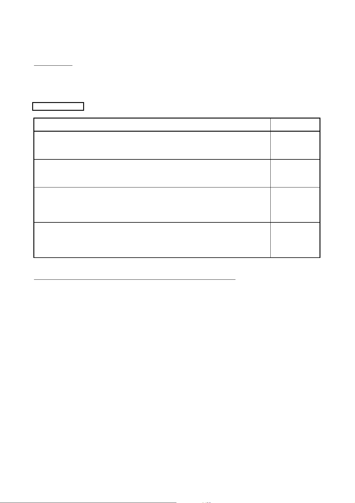
About Manuals
The following manuals are also related to this product.
In necessary, order them by quoting the details in the tables below.
Related Manuals
Manual Name
Basic model QCPU (Q Mode) User's M anual (Hardware Design/Maintenance and Inspection)
This manual provides the specifications of the CPU modules, power supply modules, base units, extension
cables, memory cards and others. (Optional)
Manual Number
(Model Code)
SH-080187
(13JR43)
Basic model QCPU (Q Mode) User's M anual (Function Explanation/Program Fundamentals)
This manual explains the functions, programming methods, devices and so on necessary to create programs
with the QCPU (Q mode). (Optional)
High Performance model QCPU (Q Mode) User's M anual (H ardw are D esign/Maintenance and
Inspection)
This manual provides the specifications of the CPU modules, power supply modules, base units, extension
cables, memory cards and others. (Optional)
High Performance model QCPU (Q Mode) User's M anual (Function Explanation/Program
Fundamentals)
This manual explains the functions, programming methods, devices and so on necessary to create programs
with the QCPU (Q mode). (Optional)
SH-080188
(13JR44)
SH-080037
(13JL97)
SH-080038
(13JL98)
Conformation to the EMC Directive and Low Voltage Instruction
For details on making Mitsubishi PLC conform to the EMC directive and low voltage instruction when installing
it in your product, please refer to Chapter 3, "EMC Directive and Low Voltage Instruction" of the PLC CPU
User's Manual(Hardware).
The CE logo is printed on the rating plate on the main body of the PLC that conforms to the EMC directive and
low voltage instruction.
A - 10 A - 10
Page 12
1 GENERAL SPECIFICATIONS OF INPUT AND OUTPUT MODULES AND
INSTRUCTIONS FOR SELECTING THEM
MELSEC-Q
1. GENERAL SPECIFICATIONS OF INPUT AND OUTPUT MODULES AND INSTRUCTIONS FOR SELECTING THEM
This chapter describes the general specifications of I/O modules and instructions for
selecting them.
1.1 General Specifications
Refer to the following manual for the general specifications of the I/O modules.
• Basic model QCPU (Q Mode) User's Manual (Hardware Design/Maintenance and
Inspection)
• High Performance model QCPU (Q Mode) User's Manual (Hardware Design/
Maintenance and Inspection)
1.2 Selecting Instructions
(1) If an output module drives an inductive load, it must be switched ON for 1 second
or longer and switched OFF for 1 second or longer.
(2) If a counter or timer which has a DC-DC converter as a load is used with an output
module, using an average current to choose an output module can cause a fault
due to periodic rush currents when it is turned ON or during operation.
To reduce the influence of rush currents for use of the above load, connect a
resistor or an inductance to the load in series or use a module whose maximum
load current is larger.
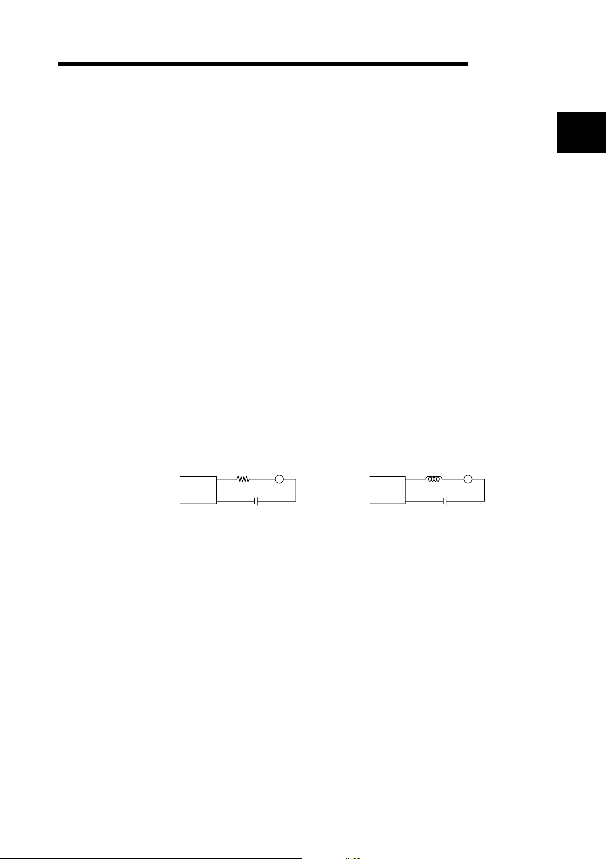
Resistor Load Inductance
Output
module
(3) Fuses installed in output modules cannot be replaced. They are designed to protect
external wiring if the module outputs are shorted.
Therefore, output modules may not be protected from a short circuit.
If an output module becomes faulty due to any cause other than a short circuit, its
fuse may not function.
(4) The number of signals, which can be turned ON simultaneously in an input module,
varies according to the input voltage and ambient temperature.
Refer to the corresponding input module specifications.
Output
module
Load
1
1 - 1 1 - 1
Page 13
1 GENERAL SPECIFICATIONS OF INPUT AND OUTPUT MODULES AND
INSTRUCTIONS FOR SELECTING THEM
1
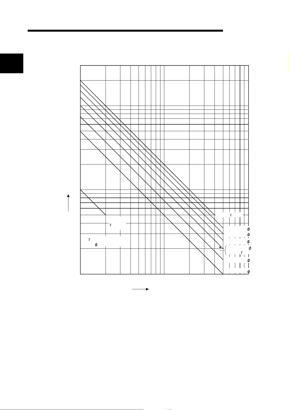
(5) The following chart shows the service life of a relay output module.
Applicable module: QY10, QY18A
MELSEC-Q
200
100
70
50
30
20
10
Switching life (10,000 times)
7
5
3
(L/R): Time constant
cos : Power factor
2
DC100
=7ms
DC30V =0ms
AC100V cos =0.7
AC200V cos =0.7
AC100V cos =0.35
AC200V cos =0.35
DC24V =7ms
AC120V cos =0.2
1
0.1 0.2 0.3 0.5 0.7 1 2 3 5
Switching current (A)
AC240V cos =0.2
1 - 2 1 - 2
Page 14
1 GENERAL SPECIFICATIONS OF INPUT AND OUTPUT MODULES AND
INSTRUCTIONS FOR SELECTING THEM
POINT
(1) When using the module for the application in which the relay contact is
frequently switched, the relay life span should be considered. Therefore, it is
recommended to use a triac output module.
(2) The relay life curve shows the value based on actual use, which is not
guaranteed. Therefore, make sure to allow for a margin of error.
The relay life span differs according to the specifications as follows:
Rated switching voltage, current load 100 thousand operations
200V AC 1.5A, 240V AC 1A (COS
200V AC 0.4A, 240V AC 0.3A (COS
200V AC 1A, 240V AC 0.5A (COS
200V AC 0.3A, 240V AC 0.15A (COS
24V DC 1A, 100V DC 0.1A (L/R=7ms) 100 thousand operations
24V DC 0.3A, 100V DC 0.03A (L/R=7ms) 300 thousand operations
(3) Relay life is substantially affected by the load type and inrush current
characteristics.
The inrush current may cause the contact welding. Therefore, consideration
should be given to it as well as constant current.
(a) Inductive load
When the inductive load such as electromagnetic contactor or solenoid is
shut off, high counter-electromotive force is generated between the
contacting materials to produce an arc discharge. Consideration should be
made especially when the power factor is low, as it may decrease the life
period.
In addition, make sure to consider the contact melting, as the inrush current
equivalent to 5 to 15 times of constant current flows when the module is
powered on.
(b) Lamp load
Make sure to consider the contact melting, as the inrush current equivalent
to 10 to 15 times of constant current flows in the lamp circuit.
(c) Capacitive load
Make sure to consider the contact melting when a device such as condenser
is used in a load circuit, as the inrush current equivalent to 20 to 40 times of
constant current may flow in the circuit.
Also, pay full attention to the wire capacity if long length of wire is routed.
(6) Insulation-sleeved crimping terminals cannot be used with the terminal block.
It is recommended to cover the wire connections of the crimping terminals with
mark or insulation tubes.
(7) Use wires of 0.3 to 0.75mm
terminal block.
(8) Do not use I/O modules under pressure higher than the atmospheric pressure of
0m (0ft.) altitude. Doing so can cause a malfunction.
When using I/O modules under pressure, please consult your sales representative.
=0.7) 100 thousand operations
=0.7) 300 thousand operations
=0.35) 100 thousand operations
=0.35) 300 thousand operations
2
core and 2.8mm (0.11in.) OD max. to connect to the
MELSEC-Q
1 - 3 1 - 3
Page 15
1 GENERAL SPECIFICATIONS OF INPUT AND OUTPUT MODULES AND
INSTRUCTIONS FOR SELECTING THEM
(9) Tighten the module fixing and terminal block screws to the torques in the following
ranges.
Screw Location Tightening Torque Range
Module fixing screw (M3 12 screw) 36 to 48 N•cm
I/O module terminal block screw (M3 screw) 42 to 58 N•cm
I/O module terminal block mounting screw (M3 screw) 66 to 89 N•cm
(10)There are the following restrictions on the thermal protections activated by
protected output modules.
The thermal protections are overload and overheat protective functions.
(a) QY40P, QY41P, QY42P, QH42P
Function Description
Common
(Overload and overheat
protective functions)
Overload protective
function
Overheat protective
function
• If an overcurrent keeps flowing due to overload, heat is generated
to activate the overheat protective function.
• Each protective function is designed to protect the internal
elements of the module, not the external equipment.
• The overload protective function is activated in 1 point increments
in terms of 1A to 3A/point.
• The overload protective function returns operation to normal when
the load becomes a rated load
• The overheat protective function is activated in 1 point increments.
• The overheat protective function automatically returns operation to
normal when heat reduces.
MELSEC-Q
1 - 4 1 - 4
Page 16
1 GENERAL SPECIFICATIONS OF INPUT AND OUTPUT MODULES AND
INSTRUCTIONS FOR SELECTING THEM
(b) QY81P
Function Description
Common
(Overload and overheat
protective functions)
Overload protective
function
Overheat protective
function
• If an overcurrent keeps flowing due to overload, heat is generated
to activate the overheat protective function.
• Each protective function is designed to protect the internal
elements of the module, not the external equipment.
• The overload protective function is activated in 1 point increments
in terms of 1A to 3A/point.
• The overload protective function returns operation to normal when
the load becomes a rated load.
• The overheat protective function is activated in 2 point increments.
(It is activated in 2 point increments of Y0/Y1, Y2/Y 3, ..., and w hen
overheat protection is activated, that of 2 points is activated
simultaneously. If an overheat condition persists, heat transferred
may activate the other overheat protective function.)
• If an output turns ON at the activation of the overheat protective
function, the actual output voltage oscillates between 0V and load
voltage.
At the load voltage of 24V, the average voltage during oscillation is
approx. 7V.
No oscillation is encountered when the output is OFF at the
activation of the overheat protective function.
To ensure that the output is turned OFF at the activation of the
overheat protective function, use an external load which sw itches
OFF at 7V or more.
• The overheat protective function automatically returns operation to
normal when heat reduces.
(11)Input modules may import noise or the like as an input depending on the pulse
width of a signal.
This pulse width has a value as listed below depending on the parameter-set
response time. The operating environment should be fully considered when making
the response time setting.
Response Time Setting (ms)
1 0.3
5 3
10 6
20 12
70 45
Minimum Value of Pulse Width
That May Be Imported (ms)
MELSEC-Q
1 - 5 1 - 5
Page 17
1 GENERAL SPECIFICATIONS OF INPUT AND OUTPUT MODULES AND
INSTRUCTIONS FOR SELECTING THEM
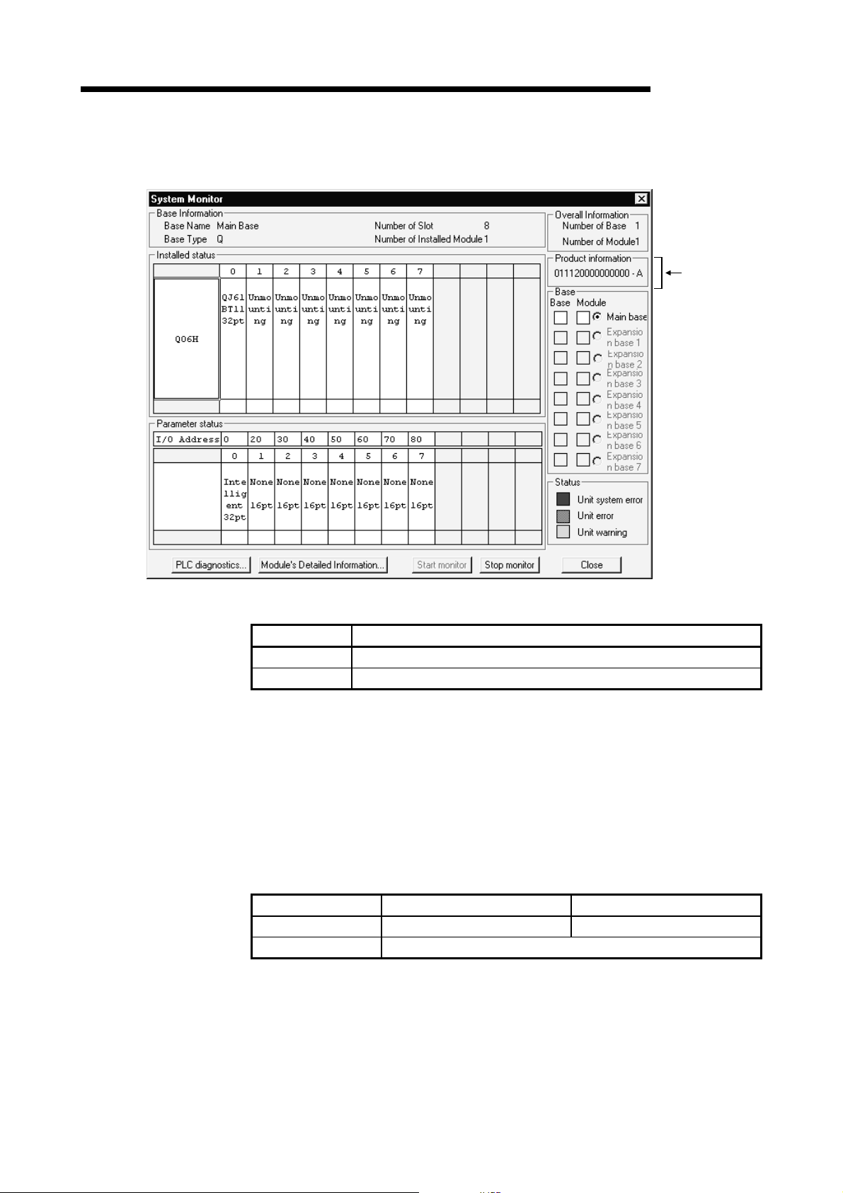
(12)When confirming the product information on the CPU PLC, observe the system
monitor in the DIAGNOSIS menu of the GX Developer.
MELSEC-Q
Confirm by
observing here.
(13)When using the QH42P or QX48Y57, configure it with the following devices.
Part name Detail
CPU PLC Product of product information [011120000000000-A] or later
GX Developer
SW5D5C-GPPW or later
The CPU PLCs other than those listed above cannot be used.
When the SW4D5C-GPPW is used, the response time cannot be set
(fixed at 10ms).
Set OUTPUT for the I/O allocation.
(14)Instructions for use of QY22
It is recommended to fit a fuse to each external terminal in order to prevent the
external device and module from being burnt if a load short-circuit occurs.
The fuse recommended for fitting is the one conforming to IEC60127 Sheet 1.
The following fuses have been confirmed by Mitsubishi to operate properly.
Fuse Model 216 02.5 216 002
Rated current 2.5A 2A
Manufacturer Littelfuse, Inc
1 - 6 1 - 6
Page 18
1 GENERAL SPECIFICATIONS OF INPUT AND OUTPUT MODULES AND
INSTRUCTIONS FOR SELECTING THEM
(15) Caution points when using QY68A
Installing a fuse to the external terminal to prevent burn out of external devices and
modules in the case of a load short is recommended.
A rated voltage 3A fast type fuse is recommended.
Fuses confirmed for operation by this company are listed below.
Fuse Model 216 3.15 312 003
Rated current 3.15A 3A
Manufacturer Littelfuse, Inc
(16) Possible constructions for QI60 compatible time settings
When setting compatible times for QI60, use the constructions listed below.
If using other constructions, compatible times can not be set. (Fixed at 0.2 ms)
Product name Contents
PLC CPU Product information "021120000000000-B" or later
GX Developer SW6D5C-GPPW or later
MELSEC-Q
1 - 7 1 - 7
Page 19
1 GENERAL SPECIFICATIONS OF INPUT AND OUTPUT MODULES AND
INSTRUCTIONS FOR SELECTING THEM
1.3 How to Make Settings on GX Developer
This section describes how to make settings using GX Developer.
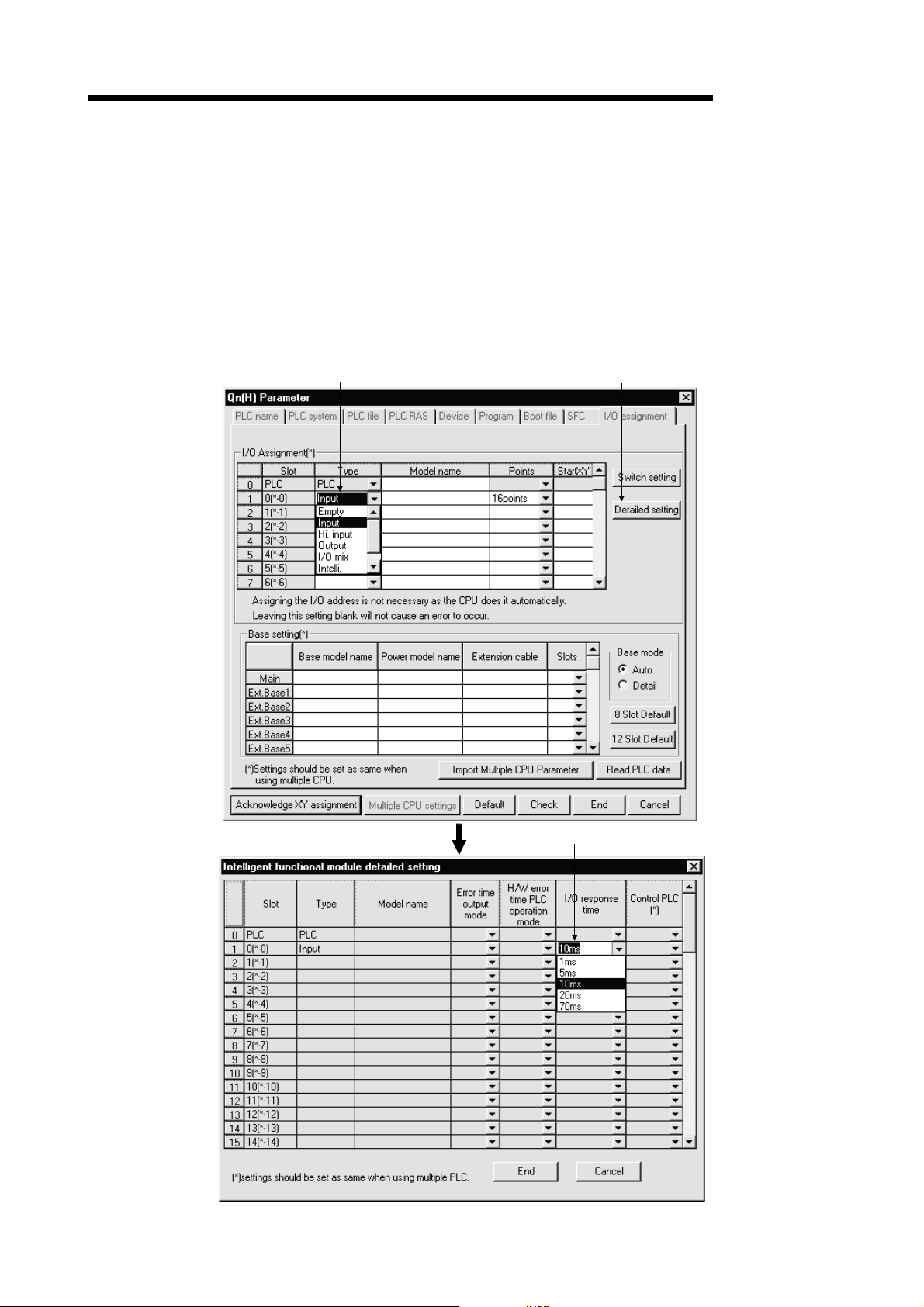
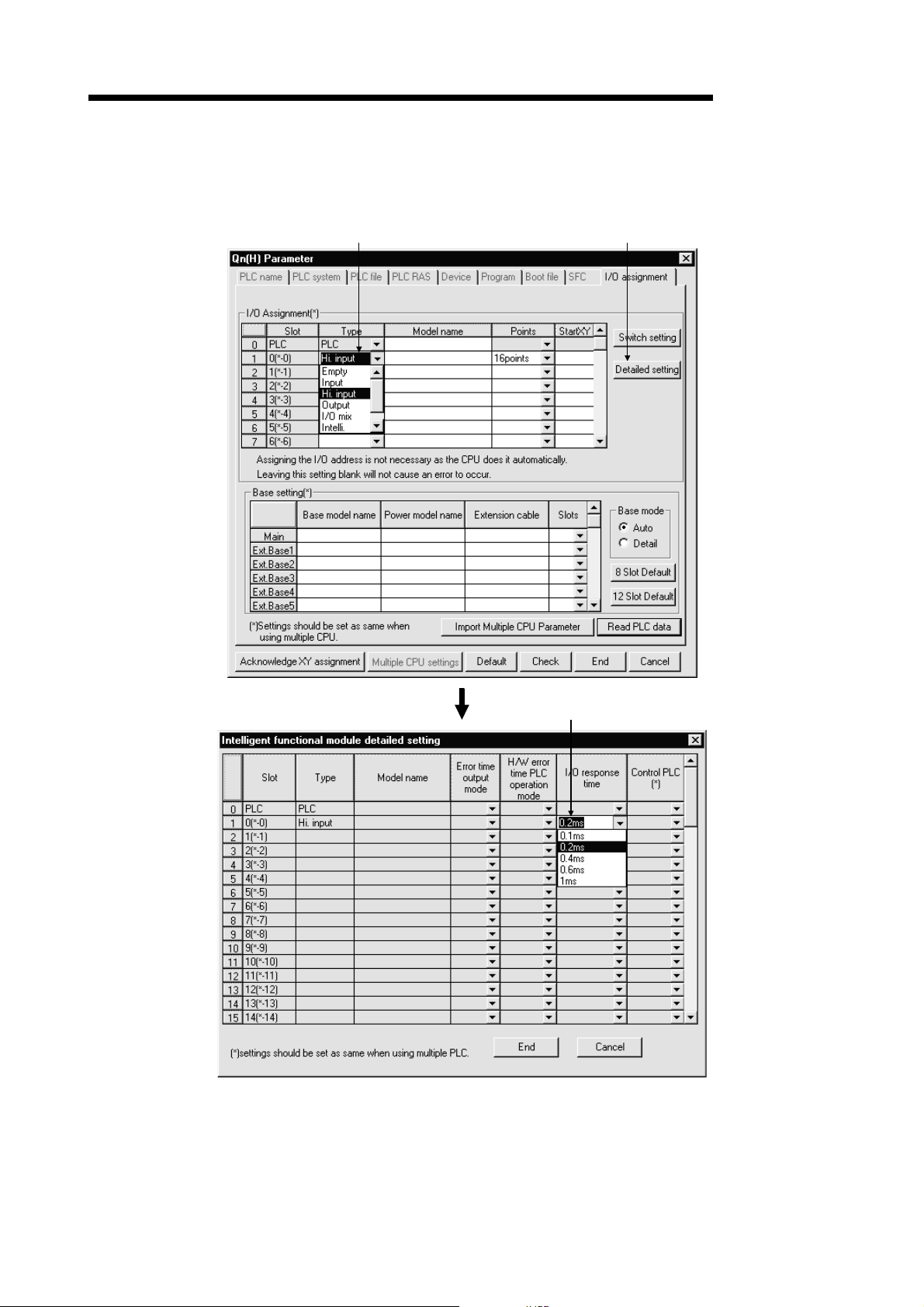
1.3.1 Setting of I/O response time
Set the I/O response time in I/O assignment of PLC Parameter.
(1) For Input/I/O mix module
Choose [Input/I/O mix] in Type, choose [Detailed setting], and choose [I/O response
time] in I/O response time.
Choose Input/I/O mix.
Choose Detailed setting.
MELSEC-Q
Choose I/O response time
1 - 8 1 - 8
(default: 10ms).
Page 20
1 GENERAL SPECIFICATIONS OF INPUT AND OUTPUT MODULES AND
INSTRUCTIONS FOR SELECTING THEM
(2) For high-speed input module/QI60
Choose [Hi. input/Interrupt] in Type, choose [Detailed setting], and choose [I/O
response time] in I/O response time.
Choose Hi. input/Interrupt. Choose Detailed setting.
MELSEC-Q
Choose I/O response time
(default: 0.2ms).
1 - 9 1 - 9
Page 21
1 GENERAL SPECIFICATIONS OF INPUT AND OUTPUT MODULES AND
INSTRUCTIONS FOR SELECTING THEM
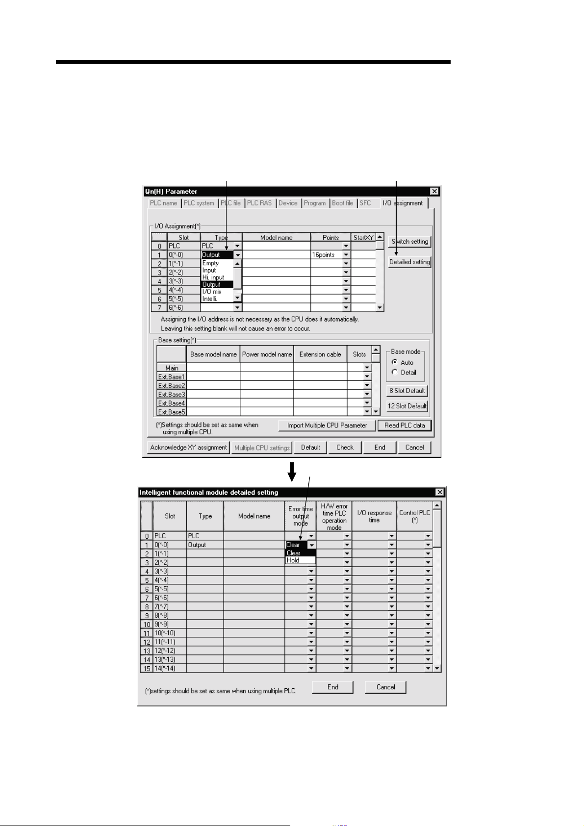
1.3.2 Setting of error-time output mode
Set the error-time output mode in I/O assignment of PLC Parameter.
Choose [Output/I/O mix] in Type, choose [Detailed setting], and choose [Clear/Hold] in
Error time output mode.
Choose Output/I/O mix. Choose Detailed setting.
MELSEC-Q
Choose Clear/Hold
(default: Clear).
1 - 10 1 - 10
Page 22
1 GENERAL SPECIFICATIONS OF INPUT AND OUTPUT MODULES AND
INSTRUCTIONS FOR SELECTING THEM
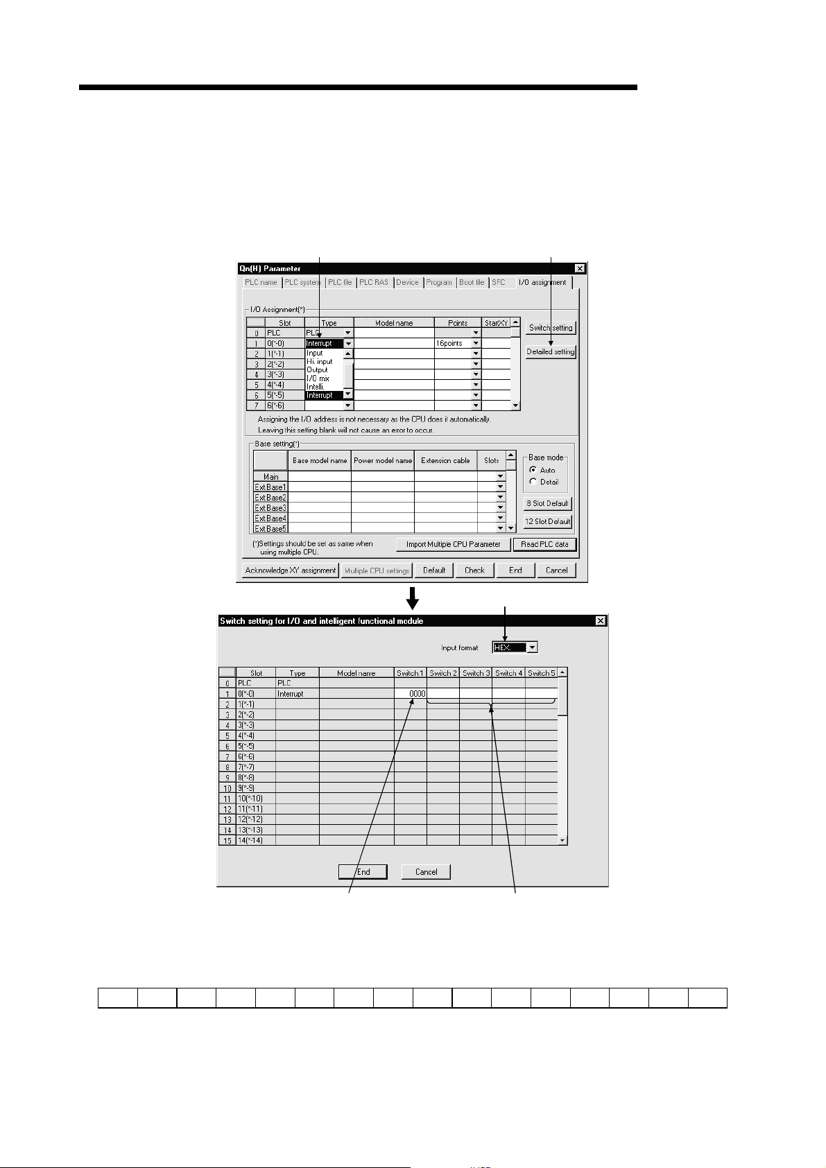
1.3.3 QI60 switch setting
Set the QI60 switches in I/O assignment of PLC Parameter.
Choose [Interrupt] in Type, choose [Switch setting], choose [HEX.] in Input format, and
set the interrupt processing conditions in Switch 1.
Choose Interrupt. Choose Switch setting.
MELSEC-Q
Choose HEX.
Set the interrupt processing conditions
(leading edge/trailing edge) of CH1 to CH16.
Setting inhibited.
Set the interrupt processing condition with switch 1. The relationships between bits and inputs are as indicated
below.
X15 X14 X13 X12 X11 X10 X9 X8 X7 X6 X5 X4 X3 X2 X1 X0
b0b15 to
0: Leading edge, 1: Trailing edge
1 - 11 1 - 11
Page 23

1 GENERAL SPECIFICATIONS OF INPUT AND OUTPUT MODULES AND
INSTRUCTIONS FOR SELECTING THEM
MELSEC-Q
MEMO
1 - 12 1 - 12
Page 24
2 INPUT MODULE SPECIFICATIONS
MELSEC-Q
2. INPUT MODULE SPECIFICATIONS
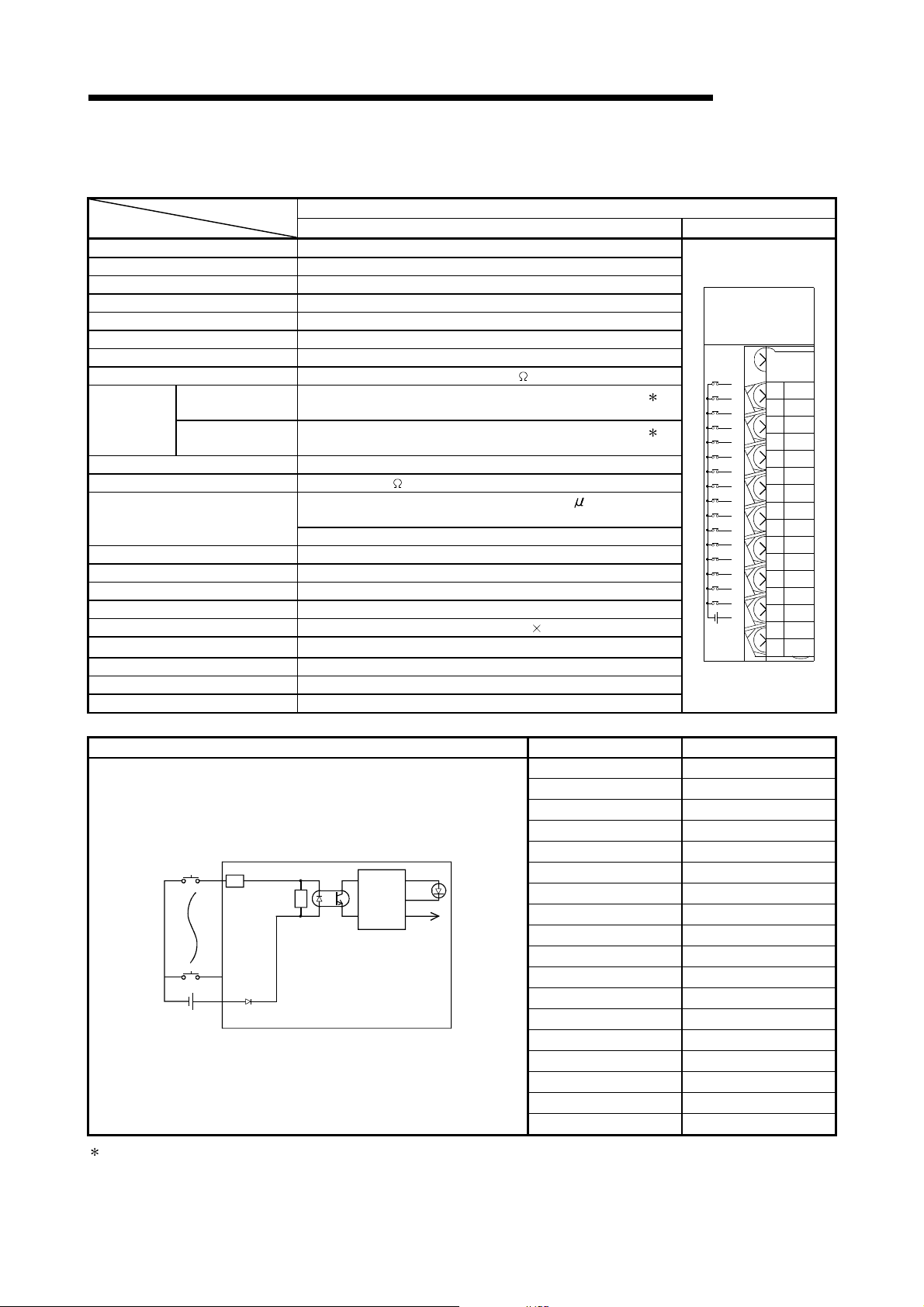
2.1 QX10 AC Input Module
Specifications
Number of input points 16 points
Isolation method Photocoupler
Rated input voltage, frequency 100-120VAC (+10/-15%) 50/60Hz (±3Hz) (distortion factor within 5%)
Rated input current Approx . 8mA (100VAC, 60Hz), approx. 7mA (100VAC, 50Hz)
Input derating Refer to the derating chart.
Inrush current Max. 200mA within 1ms (at 132VAC)
ON voltage/ON current 80VAC or higher/5mA or higher (50Hz, 60Hz)
OFF voltage/OFF current 30VAC or lower/1.7mA or lower (50Hz, 60Hz)
Input impedance Approx. 12k (60Hz), approx. 15k (50Hz)
time
Dielectric withstand voltage 1780VAC rms/3 cycles (altitude 2000m (6557.38ft.))
Insulation resistance 10M or more by insulation resistance tester
Noise immunity
Protection of degree IP1X
Common terminal arrangement 16 points/common (common terminal: TB17)
Number of I/O points 16 (I/O allocation is set as a 16-points input module)
Operation indicator ON indication (LED)
External connections 18-point terminal block (M3 6 screws)
Applicable wire size
Applicable crimping terminal R1.25-3 (sleeved crimping terminals cannot be used.)
5VDC internal current
consumption
OFF to ON 15ms or less (100VAC 50Hz, 60Hz) Response
ON to OFF 20ms or less (100VAC 50Hz, 60Hz)
By noise simulator of 1500Vp-p noise voltage, 1 s noise width
and 25 to 60Hz noise frequency
First transient noise IEC61000-4-4: 1kV
0.3 to 0.75mm
50mA (TYP. all points ON)
Weight 0.17kg
QX10 Appearance
2
core (2.8mm (0.11in.) OD max.)
Derating Chart Terminal Block Number Signal Name
(%)
100
90
80
ON
ratio
70
60
50
40
0102030405055
Ambient temperature
External Connections TB8 X07
TB 1
R
R
R
TB16
TB17
100VAC
Internal
circuit
120VAC
132VAC
( )
C
LED
AC Input Module Type
TB1 X00
TB2 X01
TB3 X02
TB4 X03
TB5 X04
TB6 X05
TB7 X06
TB9 X08
TB10 X09
TB11 X0A
TB12 X0B
TB13 X0C
TB14 X0D
TB15 X0E
TB16 X0F
TB17 COM
TB18 Vacant
QX10
01234567
89 ABCDEF
0
1
2
3
4
5
6
7
8
9
A
B
C
D
E
F
COM
NC
100VAC
8mA60Hz
7mA50Hz
2
0
1
2
3
4
5
6
7
8
9
A
B
C
D
E
F
2 - 1 2 - 1
Page 25

V
V
2 INPUT MODULE SPECIFICATIONS
2.2 QX28 AC Input Module
MELSEC-Q
2
AC Input Module Type
Specifications
QX28 Appearance
Number of input points 8 points
Isolation method Photocoupler
Rated input voltage, frequency 100-240VAC (+10/-15%) 50/60Hz (±3Hz) (distortion factor within 5%)
Rated input current
Approx. 17mA (200VAC, 60Hz), approx. 14mA (200VAC, 50Hz)
Approx. 8mA (100VAC, 60Hz), approx. 7mA (100VAC, 50Hz)
Input derating Refer to the derating chart.
Inrush current Max. 500mA within 1ms (at 264VAC)
ON voltage/ON current 80VAC or higher/5mA or higher (50Hz, 60Hz)
OFF voltage/OFF current 30VAC or lower/1.7mA or lower (50Hz, 60Hz)
Input impedance Approx. 12k (60Hz), approx. 15k (50Hz)
OFF to ON 10ms or less (100VAC 50Hz, 60Hz) Response
time
ON to OFF 20ms or less (100VAC 50Hz, 60Hz)
Dielectric withstand voltage 2830VAC rms/3 cycles (altitude 2000m (6557.38ft.))
Insulation resistance 10M or more by insulation resistance tester
By noise simulator of 1500Vp-p noise voltage, 1 s noise width
Noise immunity
and 25 to 60Hz noise frequency
First transient noise IEC61000-4-4: 1kV
Protection of degree IP1X
Common terminal arrangement 8 points/common (common terminal: TB17)
Number of I/O points 16 (I/O allocation is set as a 16-points input module)
Operation indicator ON indication (LED)
External connections 18-point terminal block (M3 6 screws)
Applicable wire size
0.3 to 0.75mm
2
core (2.8mm (0.11in.) OD max.)
Applicable crimping terminal R1.25-3 (sleeved crimping terminals cannot be used.)
5VDC internal current
consumption
50mA (TYP. all points ON)
Weight 0.20kg
Derating Chart Terminal Block Number Signal Name
ON
ratio
(%)
100
90
80
70
100% 45 C
100% 55 C
87.5% 55
240
264
C
60
50
40
0102030405055
Ambient temperature
( )
C
External Connections TB8 Vacant
TB 1
TB15
TB17
100/200AC
R
R
R
Internal
circuit
LED
TB1 X00
TB2 Vacant
TB3 X01
TB4 Vacant
TB5 X02
TB6 Vacant
TB7 X03
TB9 X04
TB10 Vacant
TB11 X05
TB12 Vacant
TB13 X06
TB14 Vacant
TB15 X07
TB16 Vacant
TB17 COM
TB18 Vacant
QX28
01234567
0
NC
1
NC
2
NC
3
NC
4
NC
5
NC
6
NC
7
MC
COM
NC
200VAC
17mA60Hz
14mA50Hz
0
1
2
3
4
5
6
7
8
9
A
B
C
D
E
F
2 - 2 2 - 2
Page 26
2 INPUT MODULE SPECIFICATIONS
2.3 QX40 DC Input Module (Positive Common Type)
DC Input Module (Positive Common Type) Type
Specifications
Number of input points 16 points
Isolation method Photocoupler
Rated input voltage 24VDC (+20/-15%, ripple ratio within 5%)
Rated input current Approx. 4mA
Input derating No
ON voltage/ON current 19V or higher/3mA or higher
OFF voltage/OFF current 11V or lower/1.7mA or lower
Input impedance Approx. 5.6k
1ms/5ms/10ms/20ms/70ms or less (CPU parameter setting)
1ms/5ms/10ms/20ms/70ms or less (CPU parameter setting)
Response
time
OFF to ON
ON to OFF
Dielectric withstand voltage 560VAC rms/3 cycles (altitude 2000m (6557.38ft.))
Insulation resistance 10M or more by insulation resistance tester
By noise simulator of 500Vp-p noise voltage, 1 s noise width
Noise immunity
and 25 to 60Hz noise frequency
First transient noise IEC61000-4-4: 1kV
Protection of degree IP2X
Common terminal arrangement 16 points/common (common terminal: TB17)
Number of I/O points 16 (I/O allocation is set as a 16-points input module)
Operation indicator ON indication (LED)
External connections 18-point terminal block (M3 6 screws)
Applicable wire size
0.3 to 0.75mm
Applicable crimping terminal R1.25-3 (sleeved crimping terminals cannot be used.)
5VDC internal current consumption 50mA (TYP. all points ON)
Weight 0.16kg
External Connections Terminal Block Number Signal Name
TB 1
R
R
TB16
TB17
24VDC
Internal
circuit
: For the setting method, refer to the section 1.3.1.
QX40 Appearance
Initial setting is 10ms.
Initial setting is 10ms.
2
core (2.8mm (0.11in.) OD max.)
LED
MELSEC-Q
QX40
01234567
89ABCDEF
0
0
1
2
2
4
3
4
6
5
6
8
7
A
8
9
C
A
B
E
C
D
E
F
+-
COM
24VDC
4mA
1
3
5
7
9
B
D
F
NC
TB1 X00
TB2 X01
TB3 X02
TB4 X03
TB5 X04
TB6 X05
TB7 X06
TB8 X07
TB9 X08
TB10 X09
TB11 X0A
TB12 X0B
TB13 X0C
TB14 X0D
TB15 X0E
TB16 X0F
TB17 COM
TB18 Vacant
2 - 3 2 - 3
Page 27
2 INPUT MODULE SPECIFICATIONS
2.4 QX40-S1 DC Input Module (Positi ve Common Type)
DC Input Module (Positive Common Type) Type
Specifications
Number of input points 16 points
Isolation method Photocoupler
Rated input voltage 24VDC (+20/-15%, ripple ratio within 5%)
Rated input current Approx. 6mA
Input derating No
ON voltage/ON current 19V or higher/4.0mA or higher
OFF voltage/OFF current 11V or lower/1.7mA or lower
Input impedance Approx. 3.9k
Set value 1 0.1 0.2 0.4 0.6 1
Response
time
OFF to ON
ON to OFF
Typ 0.05ms 0.15ms 0.30ms 0.55ms 1.05ms
max 0.10ms 0.20ms 0.40ms 0.60ms 1.20ms
Typ 0.15ms 0.20ms 0.35ms 0.60ms 1.10ms
max 0.20ms 0.30ms 0.50ms 0.70ms 1.30ms
Dielectric withstand voltage 560VAC rms/3 cycles (altitude 2000m (6557.38ft.))
Insulation resistance 10M or more by insulation resistance tester
By noise simulator of 500Vp-p noise voltage, 1 s noise width
Noise immunity
and 25 to 60Hz noise frequency
First transient noise IEC61000-4-4: 1kV
Protection of degree IP2X
Common terminal arrangement 16 points/common (common terminal: TB17)
Number of I/O points 16 (I/O allocation is set as a 16-points Hi. input module)
Operation indicator ON indication (LED)
External connections 18-point terminal block (M3 6 screws)
Applicable wire size
0.3 to 0.75mm
Applicable crimping terminal R1.25-3 (sleeved crimping terminals cannot be used.)
5VDC internal current
consumption
Weight 0.20kg
External Connections Terminal Block Number Signal Name
TB 1
R
R
TB16
TB17
24VDC
Internal
circuit
1: CPU parameter setting. (Initial setting is 0.2ms)
Response time can be changed on SW5D5C-GPPW or later.
For the setting method, refer to the section 1.3.1.
QX40-S1 Appearance
2
core (2.8mm (0.11in.) OD max.)
60mA (TYP. all points ON)
LED
MELSEC-Q
QX40-S1
01234567
89ABCDEF
0
0
1
2
2
4
3
4
6
5
6
8
7
A
8
9
C
A
B
E
C
D
E
F
+-
COM
24VDC
6mA
1
3
5
7
9
B
D
F
NC
TB1 X00
TB2 X01
TB3 X02
TB4 X03
TB5 X04
TB6 X05
TB7 X06
TB8 X07
TB9 X08
TB10 X09
TB11 X0A
TB12 X0B
TB13 X0C
TB14 X0D
TB15 X0E
TB16 X0F
TB17 COM
TB18 Vacant
2 - 4 2 - 4
Page 28
2 INPUT MODULE SPECIFICATIONS
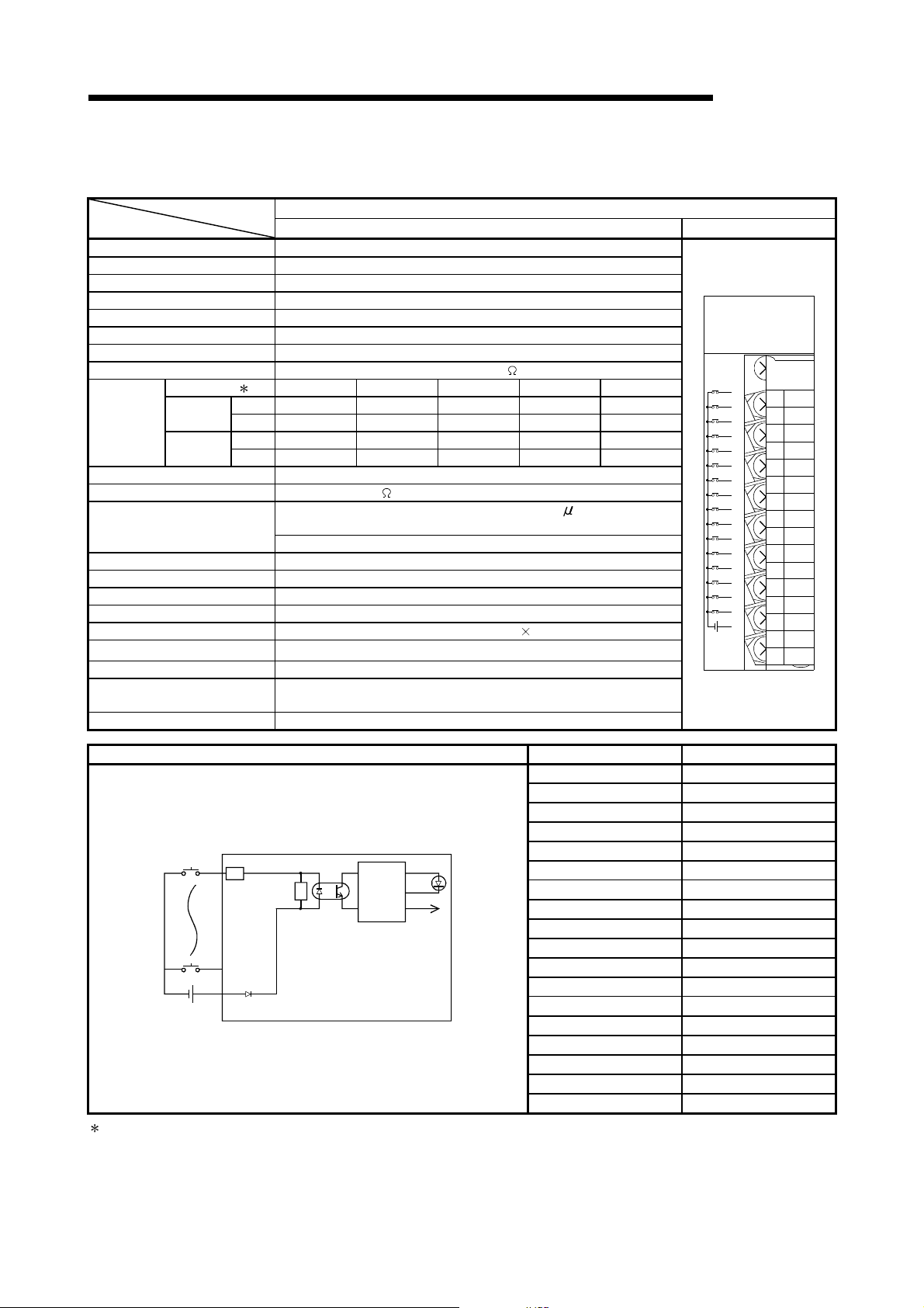
2.5 QX41 DC Input Module (Positive Common Type)
DC Input Module (Positive Common Type) Type
Specifications
Number of input points 32 points
Isolation method Photocoupler
Rated input voltage 24VDC (+20/-15%, ripple ratio within 5%)
Rated input current Approx. 4mA
Input derating Refer to the derating chart.
ON voltage/ON current 19V or higher/3mA or higher
OFF voltage/OFF current 11V or lower/1.7mA or lower
Input impedance Approx. 5.6k
1ms/5ms/10ms/20ms/70ms or less (CPU parameter setting)
1ms/5ms/10ms/20ms/70ms or less (CPU parameter setting)
Response
time
OFF to ON
ON to OFF
Dielectric withstand voltage 560VAC rms/3 cycles (altitude 2000m (6557.38ft.))
Insulation resistance 10M or more by insulation resistance tester
By noise simulator of 500Vp-p noise voltage, 1 s noise width
Noise immunity
and 25 to 60Hz noise frequency
First transient noise IEC61000-4-4: 1kV
Protection of degree IP2X
Common terminal arrangement 32 points/common (common terminal: B01, B02)
Number of I/O points 32 (I/O allocation is set as a 32-points input module)
Operation indicator ON indication (LED)
External connections 40-pin connector
Applicable wire size
0.3mm
2
External wiring connector A6CON1, A6CON2, A6CON3, A6CON4 (optional)
Applicable connector/terminal block
conversion module
A6TBXY36, A6TBXY54, A6TBX70
5VDC internal current consumption 75mA (TYP. all points ON)
Weight 0.15kg
Derating Chart Pin-Outs Pin No. Signal No. Pin No. Signal No.
(%)
100
90
80
ON
ratio
70
28.8VDC
60
50
40
0102030405055
Ambient temperature
( )
C
External Connections B11 X09 A11 X19
LED
Module front view
24VDC
B20
A05
B02
B01
R
R
Internal
circuit
: For the setting method, refer to the section 1.3.1.
1
: When using A6CON2 or A6CON3, refer to Chapter 7.
2
QX41 Appearance
Initial setting is 10ms.
Initial setting is 10ms.
(For A6CON1 or A6CON4) 2
B20 X00 A20 X10
B19 X01 A19 X11
B18 X02 A18 X12
B20
B19
B18
B17
B16
B15
B14
B13
B12
B11
B10
B9
B8
B7
B6
B5
B4
B3
B2
B1
A20
A19
A18
A17
A16
A15
A14
A13
A12
A11
A10
A9
A8
A7
A6
A5
A4
A3
A2
A1
B17 X03 A17 X13
B16 X04 A16 X14
B15 X05 A15 X15
B14 X06 A14 X16
B13 X07 A13 X17
B12 X08 A12 X18
B10 X0A A10 X1A
B09 X0B A09 X1B
B08 X0C A08 X1C
B07 X0D A07 X1D
B06 X0E A06 X1E
B05 X0F A05 X1F
B04 Vacant A04 Vacant
B03 Vacant A03 Vacant
B02 COM A02 Vacant
B01 COM A01 Vacant
MELSEC-Q
QX41
01234567
89ABCDEF
01234567
89ABCDEF
24VDC
4mA
1
1
QX41
2 - 5 2 - 5
Page 29

2 INPUT MODULE SPECIFICATIONS
2.6 QX41-S1 DC Input Module (Positi ve Common Type)
DC Input Module (Positive Common Type) Type
Specifications
Number of input points 32 points
Isolation method Photocoupler
Rated input voltage 24VDC (+20/-15%, ripple ratio within 5%)
Rated input current Approx. 4mA
Input derating Refer to the derating chart.
ON voltage/ON current 19V or higher/3.0mA or higher
OFF voltage/OFF current 9.5V or lower/1.5mA or lower
Input impedance Approx. 5.6k
Set value 1 0.1 0.2 0.4 0.6 1
Response
time
Dielectric withstand voltage 560VAC rms/3 cycles (altitude 2000m (6557.38ft.))
Common terminal arrangement 32 points/common (common terminal: B01, B02)
External wiring connector A6CON1, A6CON2, A6CON3, A6CON4 (optional)
Applicable connector/terminal
block conversion module
1: CPU parameter setting. (Initial setting is 0.2ms)
Response time can be changed on SW5D5C-GPPW or later.
For the setting method, refer to the section 1.3.1.
: When using A6CON2 or A6CON3, refer to Chapter 7.
2
OFF to ON
ON to OFF
Insulation resistance 10M or more by insulation resistance tester
Noise immunity
Protection of degree IP2X
Number of I/O points 32 (I/O allocation is set as a 32-points Hi. input module)
Operation indicator ON indication (LED)
External connections 40-pin connector
Applicable wire size
5VDC internal current
consumption
Weight 0.15kg
Typ 0.05ms 0.15ms 0.30ms 0.55ms 1.05ms
max 0.12ms 0.20ms 0.40ms 0.60ms 1.20ms
Typ 0.15ms 0.20ms 0.35ms 0.60ms 1.10ms
max 0.20ms 0.30ms 0.50ms 0.70ms 1.30ms
By noise simulator of 500Vp-p noise voltage, 1 s noise width
and 25 to 60Hz noise frequency
First transient noise IEC61000-4-4: 1kV
0.3mm
A6TBXY36, A6TBXY54, A6TBX70
QX41-S1 Appearance
2
(For A6CON1 or A6CON4) 2
75mA (TYP. all points ON)
MELSEC-Q
QX41-S1
01234567
89ABCDEF
01234567
89ABCDEF
24VDC
4mA
QX41-S1
2 - 6 2 - 6
Page 30

2 INPUT MODULE SPECIFICATIONS
Derating Chart Pin-Outs Pin No. Signal No. Pin No. Signal No.
(%)
100
90
80
ON
ratio
70
28.8VDC
60
50
40
0102030405055
Ambient temperature
( )
C
External Connections B11 X09 A11 X19
LED
24VDC
B20
A05
B02
B01
R
R
Internal
circuit
B20
B19
B18
B17
B16
B15
B14
B13
B12
B11
B10
B9
B8
B7
B6
B5
B4
B3
B2
B1
A20
A19
A18
A17
A16
A15
A14
A13
A12
A11
A10
A9
A8
A7
A6
A5
A4
A3
A2
A1
Module front view
MELSEC-Q
B20 X00 A20 X10
B19 X01 A19 X11
B18 X02 A18 X12
B17 X03 A17 X13
B16 X04 A16 X14
B15 X05 A15 X15
B14 X06 A14 X16
B13 X07 A13 X17
B12 X08 A12 X18
B10 X0A A10 X1A
B09 X0B A09 X1B
B08 X0C A08 X1C
B07 X0D A07 X1D
B06 X0E A06 X1E
B05 X0F A05 X1F
B04 Vacant A04 Vacant
B03 Vacant A03 Vacant
B02 COM A02 Vacant
B01 COM A01 Vacant
2 - 7 2 - 7
Page 31

2 INPUT MODULE SPECIFICATIONS
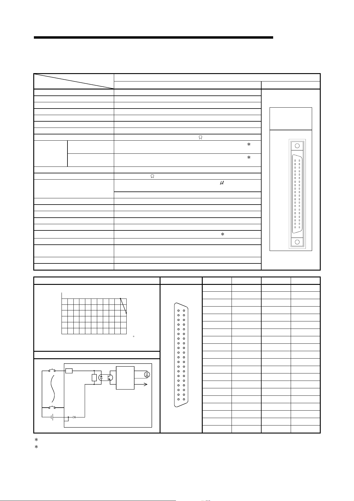
2.7 QX42 DC Input Module (Positive Common Type)
MELSEC-Q
Specifications
QX42 Appearance
Number of input points 64 points
DC Input Module (Positive Common Type) Type
Isolation method Photocoupler
Rated input voltage 24VDC (+20/-15%, ripple ratio within 5%)
Rated input current Approx. 4mA
Input derating Refer to the derating chart.
ON voltage/ON current 19V or higher/3mA or higher
OFF voltage/OFF current 11V or lower/1.7mA or lower
Input impedance Approx. 5.6k
Response
time
OFF to ON
ON to OFF
1ms/5ms/10ms/20ms/70ms or less (CPU parameter setting)
Initial setting is 10ms.
1ms/5ms/10ms/20ms/70ms or less (CPU parameter setting)
Initial setting is 10ms.
1
1
QX42
01234567
89ABCDEF
01234567
89ABCDEF
24VDC
4mA
DISPLAY
F L
QX42
Dielectric withstand voltage 560VAC rms/3 cycles (altitude 2000m (6557.38ft.))
Insulation resistance 10M or more by insulation resistance tester
By noise simulator of 500Vp-p noise voltage, 1 s noise width
Noise immunity
and 25 to 60Hz noise frequency
First transient noise IEC61000-4-4: 1kV
Protection of degree IP2X
Common terminal arrangement 32 points/common (common terminal: 1B01, 1B02, 2B01, 2B02)
Number of I/O points 64 (I/O allocation is set as a 32-points input module)
Operation indicator ON indication (LED), 32 point switch-over using switch
External connections 40-pin connector
Applicable wire size
0.3mm
2
(For A6CON1 or A6CON4) 4
External wiring connector A6CON1, A6CON2, A6CON3, A6CON4 (optional)
Applicable connector/terminal block
conversion module
A6TBXY36, A6TBXY54, A6TBX70
5VDC internal current consumption 90mA (TYP. all points ON)
(%)
100
ON
ratio
24VDC
The above diagram shows the first half of 32 points
(F).
The latter half of 32 points (L) are similar.
Weight 0.18kg
Derating Chart Pin-Outs
90
80
70
60
50
40
30
20
0102030405055
Ambient temperature
External Connections
1B20
+-
1A5
1B2
1B1
R
R
Left side
(first half)
Right side
(latter half)
SW
3
Internal
circuit
Indication
selector
circuit
24VDC
26.4VDC
28.8VDC
( )
C
LED
B20
B19
B18
B17
B16
B15
B14
B13
B12
B11
B10
B9
B8
B7
B6
B5
B4
B3
B2
B1
Module front view
Sig-
Pin
nal
No.
No.
1B20 X00 1A20 X10 2B20 X20 2A20 X30
1B19 X01 1A19 X11 2B19 X21 2A19 X31
1B18 X02 1A18 X12 2B18 X22 2A18 X32
1B17 X03 1A17 X13 2B17 X23 2A17 X33
A20
1B16 X04 1A16 X14 2B16 X24 2A16 X34
A19
A18
1B15 X05 1A15 X15 2B15 X25 2A15 X35
A17
A16
1B14 X06 1A14 X16 2B14 X26 2A14 X36
A15
1B13 X07 1A13 X17 2B13 X27 2A13 X37
A14
A13
1B12 X08 1A12 X18 2B12 X28 2A12 X38
A12
A11
1B11 X09 1A11 X19 2B11 X29 2A11 X39
A10
A9
1B10 X0A 1A10 X1A 2B10 X2A 2A10 X3A
A8
A7
1B09 X0B 1A09 X1B 2B09 X2B 2A09 X3B
A6
1B08 X0C 1A08 X1C 2B08 X2C 2A08 X3C
A5
A4
1B07 X0D 1A07 X1D 2B07 X2D 2A07 X3D
A3
A2
1B06 X0E 1A06 X1E 2B06 X2E 2A06 X3E
A1
1B05 X0F 1A05 X1F 2B05 X2F 2A05 X3F
1B04 Vacant 1A04 Vacant 2B04 Vacant 2A04 Vacant
1B03 Vacant 1A03 Vacant 2B03 Vacant 2A03 Vacant
1B02 COM 1A02 Vacant 2B02
1B01 COM 1A01 Vacant 2B01
Pin
No.
Sig-
nal
No.
Pin
No.
Sig-
nal
No.
COM2
COM2
Pin
No.
2A02 Vacant
2A01 Vacant
1: For the setting method, refer to the section 1.3.1.
2: Pin number of 1 indicates that of the left-hand side connector, and pin number of 2 indicates that of the right-hand
side connector.
3: Selection of left-hand (F) side provides the first half (X00 to X1F) LED indications, and selection of right-hand (L) side provides the
latter half (X20 to X3F) LED indications.
: When using A6CON2 or A6CON3, refer to Chapter 7.
4
Sig-
nal
No.
2 - 8 2 - 8
Page 32

2 INPUT MODULE SPECIFICATIONS
MELSEC-Q
2.8 QX42-S1 DC Input Module (Positi ve Common Type)
DC Input Module (Positive Common Type) Type
Specifications
Number of input points 64 points
Isolation method Photocoupler
Rated input voltage 24VDC (+20/-15%, ripple ratio within 5%)
Rated input current Approx. 4mA
Input derating
ON voltage/ON current 19V or higher/3.0mA or higher
OFF voltage/OFF current 9.5V or lower/1.5mA or lower
Input impedance Approx. 5.6k
Set value 1 0.1 0.2 0.4 0.6 1
Response
time
Dielectric withstand voltage 560VAC rms/3 cycles (altitude 2000m (6557.38ft.))
Common terminal arrangement
External wiring connector A6CON1, A6CON2, A6CON3, A6CON4 (optional)
Applicable connector/terminal
block conversion module
1: CPU parameter setting. (Initial setting is 0.2ms)
Response time can be changed on SW5D5C-GPPW or later.
For the setting method, refer to the section 1.3.1.
2: Pin number of 1 indicates that of the left-hand side connector, and pin number of 2 indicates that of the right-hand
side connector.
3: Selection of left-hand (F) side provides the first half (X00 to X1F) LED indications, and selection of right-hand (L) side provides the
latter half (X20 to X3F) LED indications.
: When using A6CON2 or A6CON3, refer to Chapter 7.
4
OFF to ON
ON to OFF
Insulation resistance 10M or more by insulation resistance tester
Noise immunity
Protection of degree IP2X
Number of I/O points 64 (I/O allocation is set as a 64-points Hi. input module)
Operation indicator ON indication (LED)
External connections
Applicable wire size
5VDC internal current
consumption
Weight 0.18kg
Typ 0.05ms 0.15ms 0.30ms 0.55ms 1.05ms
max 0.12ms 0.20ms 0.40ms 0.60ms 1.20ms
Typ 0.15ms 0.20ms 0.35ms 0.60ms 1.10ms
max 0.20ms 0.30ms 0.50ms 0.70ms 1.30ms
By noise simulator of 500Vp-p noise voltage, 1 s noise width
and 25 to 60Hz noise frequency
First transient noise IEC61000-4-4: 1kV
32 points/common (common terminal: 1B01, 1B02, 2B01, 2B02)
0.3mm
A6TBXY36, A6TBXY54, A6TBX70
QX42-S1 Appearance
Refer to the derating chart.
40-pin connector
2
(For A6CON1 or A6CON4) 4
90mA (TYP. all points ON)
QX42-S1
01234567
89ABCDEF
01234567
89ABCDEF
24VDC
4mA
DISPLAY
F L
QX42-S1
2 - 9 2 - 9
Page 33

2 INPUT MODULE SPECIFICATIONS
Derating Chart Pin-Outs
(%)
100
90
80
ON
70
ratio
60
50
40
30
20
0102030405055
Ambient temperature
External Connections
24VDC
1B20
+-
1A5
1B2
1B1
R
R
Left side
(first half)
Right side
(latter half)
SW
The above diagram shows the first half of 32 points
(F).
The latter half of 32 points (L) are similar.
3
Internal
circuit
Indication
selector
circuit
24VDC
26.4VDC
28.8VDC
( )
C
LED
B20
B19
B18
B17
B16
B15
B14
B13
B12
B11
B10
B9
B8
B7
B6
B5
B4
B3
B2
B1
Module front view
MELSEC-Q
Pin
No.
Sig-
nal
No.
Sig-
Pin
nal
No.
No.
1B20 X00 1A20 X10 2B20 X20 2A20 X30
1B19 X01 1A19 X11 2B19 X21 2A19 X31
1B18 X02 1A18 X12 2B18 X22 2A18 X32
1B17 X03 1A17 X13 2B17 X23 2A17 X33
A20
1B16 X04 1A16 X14 2B16 X24 2A16 X34
A19
A18
1B15 X05 1A15 X15 2B15 X25 2A15 X35
A17
A16
1B14 X06 1A14 X16 2B14 X26 2A14 X36
A15
1B13 X07 1A13 X17 2B13 X27 2A13 X37
A14
A13
1B12 X08 1A12 X18 2B12 X28 2A12 X38
A12
A11
1B11 X09 1A11 X19 2B11 X29 2A11 X39
A10
A9
1B10 X0A 1A10 X1A 2B10 X2A 2A10 X3A
A8
A7
1B09 X0B 1A09 X1B 2B09 X2B 2A09 X3B
A6
1B08 X0C 1A08 X1C 2B08 X2C 2A08 X3C
A5
A4
1B07 X0D 1A07 X1D 2B07 X2D 2A07 X3D
A3
A2
1B06 X0E 1A06 X1E 2B06 X2E 2A06 X3E
A1
1B05 X0F 1A05 X1F 2B05 X2F 2A05 X3F
1B04 Vacant 1A04 Vacant 2B04 Vacant 2A04 Vacant
1B03 Vacant 1A03 Vacant 2B03 Vacant 2A03 Vacant
1B02 COM 1A02 Vacant 2B02
1B01 COM 1A01 Vacant 2B01
Pin
No.
Sig-
nal
No.
COM2
COM2
Sig-
Pin
nal
No.
No.
2A02 Vacant
2A01 Vacant
2 - 10 2 - 10
Page 34

2 INPUT MODULE SPECIFICATIONS
MELSEC-Q
2.9 QX70 DC Input Module (Positive Common/Negative Common Shared Type)
DC Input Module (Positive Common/Negative Common Shared Type) Type
Specifications
Number of input points 16 points
Insulation method Photocoupler
Rated input voltage
(+20/-15%, ripple ratio within 5%)
5VDC
Rated input current Approx. 1.2mA Approx. 3.3mA
Input derating None
ON voltage/ON current 3.5V or higher/1mA or higher
OFF voltage/OFF current 1V or lower/0.1mA or lower
Input resistance Approx. 3.3k
1ms/5ms/10ms/20ms/70ms or less (CPU parameter setting)
1ms/5ms/10ms/20ms/70ms or less (CPU parameter setting)
Response
time
OFF ON
ON
OFF
Dielectric maximum voltage 560VAC rms/3 cycles (altitude 2000m)
Insulation resistance 10M or more by insulation resistance tester
By noise simulator of 500Vp-p noise voltage,
s noise width and 25 to 60Hz noise frequency
Noise immunity
1
First transient noise IEC61000-4-4: 0.25kV
Protection of degree IP2X
Common terminal arrangement 16 points/common (common terminal: TB17)
Number of I/O points 16 (I/O allocation is set as a 16-points input module)
Operation indicator ON indication (LED)
External connections 18-point terminal block (M3 6 screw)
Applicable wire size
Core cable: 0.3 to 0.75mm
Applicable connector terminal R1.25-3 (Terminals with sleeve cannot be used)
5VDC internal current
consumption
55mA (TYP, all points ON)
Weight 0.14kg
External Connections Terminal Block No. Signal Name
For open collector (positive common) connect io n
TB 1
R
TB17
5/12VDC
For TTL, LS-TTL, CMO S buf f er
(positive common) connections
TB 1
TB17
R
For sensor (negative common)
connections
LED
Internal
circuit
: For the setting method, refer to the section 1.3.1.
QX70 Appearance
12VDC
(+20/-15%, ripple ratio within 5%)
Initial setting is 10ms
Initial setting is 10ms
2
(Outside diameter: 2.8mm or smaller)
QX70
01234567
89ABCDEF
0
1
2
3
4
5
6
7
8
9
A
B
C
D
E
F
+-
COM
NC
5/12VDC
1.2mA
3.3mA
TB1 X00
TB2 X01
TB3 X02
TB4 X03
TB5 X04
TB6 X05
TB7 X06
TB8 X07
TB9 X08
TB10 X09
TB11 X0A
TB12 X0B
TB 1
TB13 X0C
TB14 X0D
TB15 X0E
TB16 X0F
TB17
TB17 COM
TB18 Vacant
0
1
2
3
4
5
6
7
8
9
A
B
C
D
E
F
2 - 11 2 - 11
Page 35

2 INPUT MODULE SPECIFICATIONS
MELSEC-Q
2.10 QX71 DC Input Module (Positive Common/Negative Common Shared Type)
DC Input Module (Positive Common/Negative Common Shared Type) Type
Specifications
Number of input points 32 points
Insulation method Photocoupler
Rated input voltage
(+20/-15%, ripple ratio within 5%)
5VDC
Rated input current Approx. 1.2mA Approx. 3.3mA
Input derating None
ON voltage/ON current 3.5V or higher/1mA or higher
OFF voltage/OFF current 1V or lower/0.1mA or lower
Input resistance Approx. 3.3k
1ms/5ms/10ms/20ms/70ms or less (CPU parameter setting)
1ms/5ms/10ms/20ms/70ms or less (CPU parameter setting)
Response
time
OFF ON
ON
OFF
Dielectric maximum voltage 560VAC rms/3 cycles (altitude 2000m)
Insulation resistance 10M or more by insulation resistance tester
By noise simulator of 500Vp-p noise voltage,
s noise width and 25 to 60Hz noise frequency
Noise immunity
1
First transient noise IEC61000-4-4: 0.25kV
Protection of degree IP2X
Common terminal arrangement 32 points/common (common terminal: B01, B02)
Number of I/O points 32 (I/O allocation is set as a 32-points input module)
Operation indicator ON indication (LED)
External connections 40-pin connector
Applicable wire size
0.3mm
2
External wiring connector A6CON1, A6CON2, A6CON3, A6CON4 (optional)
5VDC internal current
consumption
70mA (TYP, all points ON)
Weight 0.12kg
External Connections Pin-Outs Pin No.
For open collector (positive common) connection
B20
R
B02
B01
5/12VDC
For TTL, LS-TTL, CMOS buffer
(positive common) connections
: For the setting method, refer to the section 1.3.1.
1
: When using A6CON2 or A6CON3, refer to Chapter 7.
2
B20
B02
R
For sensor (negative common)
connections
LED
Internal
circuit
B20
B02
QX71 Appearance
12VDC
(+20/-15%, ripple ratio within 5%)
1
QX71
01234567
89ABCDEF
01234567
89ABCDEF
5/12VDC
1.2 / 3.3mA
Initial setting is 10ms
1
Initial setting is 10ms
(For A6CON1 or A6CON4) 2
Signal
No.
Pin No.
B20 X00 A20 X10
B20
B19
B18
B17
B16
B15
B14
B13
B12
B11
B10
B9
B8
B7
B6
B5
B4
B3
B2
B1
Module front view
A20
A19
A18
A17
A16
A15
A14
A13
A12
A11
A10
A9
A8
A7
A6
A5
A4
A3
A2
A1
B19 X01 A19 X11
B18 X02 A18 X12
B17 X03 A17 X13
B16 X04 A16 X14
B15 X05 A15 X15
B14 X06 A14 X16
B13 X07 A13 X17
B12 X08 A12 X18
B11 X09 A11 X19
B10 X0A A10 X1A
B09 X0B A09 X1B
B08 X0C A08 X1C
B07 X0D A07 X1D
B06 X0E A06 X1E
B05 X0F A05 X1F
B04 Vacant A04 Vacant
B03 Vacant A03 Vacant
B02 COM A02 Vacant
B01 COM A01 Vacant
QX71
Signal
No.
2 - 12 2 - 12
Page 36

2 INPUT MODULE SPECIFICATIONS
MELSEC-Q
2.11 QX72 DC Input Module (Positive Common/Negative Common Shared Type)
Specifications
QX72 Appearance
Number of input points 64 points
Insulation method Photocoupler
DC Input Module (Positive Common/Negative Common Shared Type) Type
Rated input voltage
(+20/-15%, ripple ratio within
5%)
(+20/-15%, ripple ratio within 5%)
Rated input current Approx. 1.2mA Approx. 3.3mA
Input derating None
ON voltage/ON current 3.5V or higher/3mA or higher
OFF voltage/OFF current 1V or lower/0.1mA or lower
5VDC
12VDC
QX72
01234567
89ABCDEF
01234567
89ABCDEF
5/12VDC
1.2/3.3mA
DISPLAY
F L
Input resistance Approx. 3.3k
Response
time
OFF ON
ON
OFF
1ms/5ms/10ms/20ms/70ms or less (CPU parameter setting)
Initial setting is 10ms
1ms/5ms/10ms/20ms/70ms or less (CPU parameter setting)
Initial setting is 10ms
1
1
Dielectric maximum voltage 560VAC rms/3 cycles (altitude 2000m)
Insulation resistance 10M or more by insulation resistance tester
By noise simulator of 500Vp-p noise voltage,
s noise width and 25 to 60Hz noise frequency
Noise immunity
1
First transient noise IEC61000-4-4: 0.25kV
Protection of degree IP2X
Common terminal arrangement 32 points/common (common terminal: 1B01, 1B02, 2B01, 2B02)
Number of I/O points 64 (I/O allocation is set as a 64-points input module)
Operation indicator ON indication (LED), 32-point switchover using switch
External connections 40-pin connector
Applicable wire size 0.3mm2 (For A6CON1 or A6CON4) 4
External wiring connector A6CON1, A6CON2, A6CON3, A6CON4 (optional)
5VDC internal current consumption 85mA (TYP, all points ON)
Weight 0.13kg
External Connections Pin-Outs Pin No.
For open collector (positive common) connection
1B20
R
R
3
SWLeft side
(first half)
Right side
1B20
1B02
(latter half)
For sensor
(negative common)
connections
1B02
1B01
5/12VDC
For TTL, LS-TTL, CMOS buffer
(positive common) connections
The above diagram shows the first half of
32 points (F).
The latter half of 32 points (L) are similar.
Internal
circuit
Indication
selector
circuit
1B20
1B02
LED
LED
B20
B19
B18
B17
B16
B15
B14
B13
B12
B11
B10
B9
B8
B7
B6
B5
B4
B3
B2
B1
Module
front view
A20
A19
A18
A17
A16
A15
A14
A13
A12
A11
A10
A9
A8
A7
A6
A5
A4
A3
A2
A1
Signal
Pin No.
No.
1B20 X00 1A20 X10 2B20 X20 2A20 X30
1B19 X01 1A19 X11 2B19 X21 2A19 X31
1B18 X02 1A18 X12 2B18 X22 2A18 X32
1B17 X03 1A17 X13 2B17 X23 2A17 X33
1B16 X04 1A16 X14 2B16 X24 2A16 X34
1B15 X05 1A15 X15 2B15 X25 2A15 X35
1B14 X06 1A14 X16 2B14 X26 2A14 X36
1B13 X07 1A13 X17 2B13 X27 2A13 X37
1B12 X08 1A12 X18 2B12 X28 2A12 X38
1B11 X09 1A11 X19 2B11 X29 2A11 X39
1B10 X0A 1A10 X1A 2B10 X2A 2A10 X3A
1B09 X0B 1A09 X1B 2B09 X2B 2A09 X3B
1B08 X0C 1A08 X1C 2B08 X2C 2A08 X3C
1B07 X0D 1A07 X1D 2B07 X2D 2A07 X3D
1B06 X0E 1A06 X1E 2B06 X2E 2A06 X3E
1B05 X0F 1A05 X1F 2B05 X2F 2A05 X3F
1B04 Vacant 1A04 Vacant 2B04 Vacant 2A04 Vacant
1B03 Vacant 1A03 Vacant 2B03 Vacant 2A03 Vacant
1B02 COM1 1A02 Vacant 2B02 COM2 2A02 Vacant
1B01 COM1 1A01 Vacant 2B01 COM2 2A01 Vacant
1: For the setting method, refer to the section 1.3.1.
2: Pin number of 1 indicates that of the left-hand side connector, and pin number of 2 indicates that of the right-hand
side connector.
3: Selection of left-hand (F) side provides the first half (X00 to X1F) LED indications, and selection of right-hand (L) side provides the
latter half (X20 to X3F) LED indications.
4: When using A6CON2 or A6CON3, refer to Chapter 7.
Signal
No.
Pin No.
Signal
No.
Pin No.
QX72
Signal
No.
2 - 13 2 - 13
Page 37

2 INPUT MODULE SPECIFICATIONS
2.12 QX80 DC Input Module (Neg ati v e C ommon Ty pe)
DC Input Module (Negative Common Type) Type
Specifications
Number of input points 16 points
Isolation method Photocoupler
Rated input voltage 24VDC (+20/-15%, ripple ratio within 5%)
Rated input current Approx. 4mA
Input derating No
ON voltage/ON current 19V or higher/3mA or higher
OFF voltage/OFF current 11V or lower/1.7mA or lower
Input impedance Approx. 5.6k
1ms/5ms/10ms/20ms/70ms or less (CPU parameter setting)
1ms/5ms/10ms/20ms/70ms or less (CPU parameter setting)
Response
time
OFF to ON
ON to OFF
Dielectric withstand voltage 560VAC rms/3 cycles (altitude 2000m (6557.38ft.))
Insulation resistance 10M or more by insulation resistance tester
By noise simulator of 500Vp-p noise voltage, 1 s noise width
Noise immunity
and 25 to 60Hz noise frequency
First transient noise IEC61000-4-4: 1kV
Protection of degree IP2X
Common terminal arrangement 16 points/common (common terminal: TB18)
Number of I/O points 16 (I/O allocation is set as a 16-points input module)
Operation indicator ON indication (LED)
External connections 18-point terminal block (M3 6 screws)
Applicable wire size
0.3 to 0.75mm
Applicable crimping terminal R1.25-3 (sleeved crimping terminals cannot be used.)
5VDC internal current consumption 50mA (TYP. all points ON)
Weight 0.16kg
External Connections Terminal Block Number Signal Name
TB 1
R
R
TB16
TB18
24VDC
Internal
circuit
: For the setting method, refer to the section 1.3.1.
QX80 Appearance
Initial setting is 10ms.
Initial setting is 10ms.
2
core (2.8mm (0.11in.) OD max.)
LED
MELSEC-Q
QX80
01234567
89ABCDEF
0
0
1
2
2
4
3
4
6
5
6
8
7
A
8
9
C
A
B
E
C
D
E
F
COM
24VDC
4mA
1
3
5
7
9
B
D
F
NC
TB1 X00
TB2 X01
TB3 X02
TB4 X03
TB5 X04
TB6 X05
TB7 X06
TB8 X07
TB9 X08
TB10 X09
TB11 X0A
TB12 X0B
TB13 X0C
TB14 X0D
TB15 X0E
TB16 X0F
TB17 Vacant
TB18 COM
2 - 14 2 - 14
Page 38

2 INPUT MODULE SPECIFICATIONS
MELSEC-Q
2.13 QX81 DC Input Module (Neg ati v e C ommon Ty pe)
DC Input Module (Negative Common Type) Type
Specifications
Number of input points 32 points
Isolation method Photocoupler
Rated input voltage 24VDC (+20/-15%, ripple ratio within 5%)
Rated input current Approx. 4mA
Input derating Refer to the derating chart.
ON voltage/ON current 19V or higher/3mA or higher
OFF voltage/OFF current 11V or lower/1.7mA or lower
Input impedance Approx. 5.6k
1ms/5ms/10ms/20ms/70ms or less (CPU parameter setting)
1ms/5ms/10ms/20ms/70ms or less (CPU parameter setting)
Response
time
OFF to ON
ON to OFF
Dielectric withstand voltage 560VAC rms/3 cycles (altitude 2000m (6557.38ft.))
Insulation resistance 10M or more by insulation resistance tester
By noise simulator of 500Vp-p noise voltage, 1 s noise width
Noise immunity
and 25 to 60Hz noise frequency
First transient noise IEC61000-4-4: 1kV
Protection of degree IP2X
Common terminal arrangement 32 points/common (common terminal: 17, 18, 36)
Number of I/O points 32 (I/O allocation is set as a 32-points input module)
Operation indicator ON indication (LED)
External connections 37-pin D-sub connector
Applicable wire size
0.3mm
External wiring connector A6CON1E, A6CON2E, A6CON3E (optional)
Applicable connector/terminal block
conversion module
A6TBX36-E, A6TBX54-E, A6TBX70-E
5VDC internal current consumption 75mA (TYP. all points ON)
Weight 0.16kg
Derating Chart Pin-Outs Pin No. Signal No. Pin No. Signal No.
(%)
100
90
80
ON
ratio
70
28.8VDC
60
50
40
0102030405055
Ambient temperature
( )
C
External Connections 24 X09 32 X19
18
24VDC
36
17
35
LED
R
1
R
Internal
circuit
Module front view
: For the setting method, refer to the section 1.3.1.
1
: When using A6CON2E or A6CON3E, refer to Chapter 7.
2
2 - 15 2 - 15
QX81 Appearance
QX81
01234567
89ABCDEF
01234567
89ABCDEF
24VDC
1
4mA
Initial setting is 10ms.
1
Initial setting is 10ms.
2
(For A6CON1E) 2
1 X00 9 X10
20 X01 28 X11
2 X02 10 X12
19
18
17
16
15
14
13
12
11
10
9
8
7
6
5
4
3
2
1
37
36
35
34
33
32
31
30
29
28
27
26
25
24
23
22
21
20
21 X03 29 X13
3 X04 11 X14
22 X05 30 X15
4 X06 12 X16
23 X07 31 X17
5 X08 13 X18
6 X0A 14 X1A
25 X0B 33 X1B
7 X0C 15 X1C
26 X0D 34 X1D
8 X0E 16 X1E
27 X0F 35 X1F
17 COM 37 Vacant
36 COM 19 Vacant
18 COM
QX81
Page 39

2 INPUT MODULE SPECIFICATIONS
2.14 QX82 DC Input Module (Neg ati v e C ommon Ty pe)
MELSEC-Q
Specifications
QX82 Appearance
Number of input points 64 points
DC Input Module (Negative Common Type) Type
Isolation method Photocoupler
Rated input voltage 24VDC (+20/-15%, ripple ratio within 5%)
Rated input current Approx. 4mA
Input derating Refer to the derating chart.
ON voltage/ON current 19V or higher/3mA or higher
OFF voltage/OFF current 11V or lower/1.7mA or lower
Input impedance Approx. 5.6k
Response
time
OFF to ON
ON to OFF
1ms/5ms/10ms/20ms/70ms or less (CPU parameter setting)
Initial setting is 10ms.
1ms/5ms/10ms/20ms/70ms or less (CPU parameter setting)
Initial setting is 10ms.
1
1
QX82
01234567
89ABCDEF
01234567
89ABCDEF
24VDC
4mA
DISPLAY
F L
QX82
Dielectric withstand voltage 560VAC rms/3 cycles (altitude 2000m (6557.38ft.))
Insulation resistance 10M or more by insulation resistance tester
By noise simulator of 500Vp-p noise voltage, 1 s noise width
Noise immunity
and 25 to 60Hz noise frequency
First transient noise IEC61000-4-4: 1kV
Protection of degree IP2X
Common terminal arrangement 32 points/common (common terminal: 1B01, 1B02, 2B01, 2B02)
Number of I/O points 64 (I/O allocation is set as a 32-points input module)
Operation indicator ON indication (LED), 32 point switch-over using switch
External connections 40-pin connector
Applicable wire size
0.3mm
2
(For A6CON1 or A6CON4) 4
External wiring connector A6CON1, A6CON2, A6CON3, A6CON4 (optional)
Applicable connector/terminal block
conversion module
—————
5VDC internal current consumption 90mA (TYP. all points ON)
(%)
100
ON
ratio
24VDC
The above diagram shows the first half of 32 points
(F).
The latter half of 32 points (L) are similar.
Weight 0.18kg
Derating Chart Pin-Outs
90
80
70
60
50
40
30
20
0102030405055
Ambient temperature
External Connections
1B20
1A5
1B2
1B1
R
R
Left side
(first half)
Right side
(latter half)
SW
3
Internal
circuit
Indication
selector
circuit
24VDC
26.4VDC
28.8VDC
( )
C
LED
B20
B19
B18
B17
B16
B15
B14
B13
B12
B11
B10
B9
B8
B7
B6
B5
B4
B3
B2
B1
Module front view
Sig-
Pin
nal
No.
No.
1B20 X00 1A20 X10 2B20 X20 2A20 X30
1B19 X01 1A19 X11 2B19 X21 2A19 X31
1B18 X02 1A18 X12 2B18 X22 2A18 X32
1B17 X03 1A17 X13 2B17 X23 2A17 X33
A20
1B16 X04 1A16 X14 2B16 X24 2A16 X34
A19
A18
1B15 X05 1A15 X15 2B15 X25 2A15 X35
A17
A16
1B14 X06 1A14 X16 2B14 X26 2A14 X36
A15
1B13 X07 1A13 X17 2B13 X27 2A13 X37
A14
A13
1B12 X08 1A12 X18 2B12 X28 2A12 X38
A12
A11
1B11 X09 1A11 X19 2B11 X29 2A11 X39
A10
A9
1B10 X0A 1A10 X1A 2B10 X2A 2A10 X3A
A8
A7
1B09 X0B 1A09 X1B 2B09 X2B 2A09 X3B
A6
1B08 X0C 1A08 X1C 2B08 X2C 2A08 X3C
A5
A4
1B07 X0D 1A07 X1D 2B07 X2D 2A07 X3D
A3
A2
1B06 X0E 1A06 X1E 2B06 X2E 2A06 X3E
A1
1B05 X0F 1A05 X1F 2B05 X2F 2A05 X3F
1B04 Vacant 1A04 Vacant 2B04 Vacant 2A04 Vacant
1B03 Vacant 1A03 Vacant 2B03 Vacant 2A03 Vacant
1B02 COM 1A02 Vacant 2B02
1B01 COM 1A01 Vacant 2B01
Pin
No.
Sig-
nal
No.
Pin
No.
Sig-
nal
No.
COM2
COM2
Pin
No.
2A02 Vacant
2A01 Vacant
1: For the setting method, refer to the section 1.3.1.
2: Pin number of 1 indicates that of the left-hand side connector, and pin number of 2 indicates that of the right-hand
side connector.
3: Selection of left-hand (F) side provides the first half (X00 to X1F) LED indications, and selection of right-hand (L) side provides the
latter half (X20 to X3F) LED indications.
: When using A6CON2 or A6CON3, refer to Chapter 7.
4
Sig-
nal
No.
2 - 16 2 - 16
Page 40

2 INPUT MODULE SPECIFICATIONS
MELSEC-Q
2.15 QX82-S1 DC Input Module (Negative Common Type)
DC Input Module (Negative Common Type) Type
Specifications
Number of input points 64 points
Isolation method Photocoupler
Rated input voltage 24VDC (+20/-15%, ripple ratio within 5%)
Rated input current Approx. 4mA
Input derating
ON voltage/ON current 19V or higher/3.0mA or higher
OFF voltage/OFF current 9.5V or lower/1.5mA or lower
Input impedance Approx. 5.6k
Set value 1 0.1 0.2 0.4 0.6 1
Response
time
Dielectric withstand voltage 560VAC rms/3 cycles (altitude 2000m (6557.38ft.))
Common terminal arrangement
External wiring connector A6CON1, A6CON2, A6CON3, A6CON4 (optional)
Applicable connector/terminal
block conversion module
1: CPU parameter setting. (Initial setting is 0.2ms)
Response time can be changed on SW5D5C-GPPW or later.
For the setting method, refer to the section 1.3.1.
2: Pin number of 1 indicates that of the left-hand side connector, and pin number of 2 indicates that of the right-hand
side connector.
3: Selection of left-hand (F) side provides the first half (X00 to X1F) LED indications, and selection of right-hand (L) side provides the
latter half (X20 to X3F) LED indications.
: When using A6CON2 or A6CON3, refer to Chapter 7.
4
OFF to ON
ON to OFF
Insulation resistance 10M or more by insulation resistance tester
Noise immunity
Protection of degree IP2X
Number of I/O points 64 (I/O allocation is set as a 64-points Hi. input module)
Operation indicator ON indication (LED)
External connections
Applicable wire size
5VDC internal current
consumption
Weight 0.18kg
Typ 0.05ms 0.15ms 0.30ms 0.55ms 1.05ms
max 0.12ms 0.20ms 0.40ms 0.60ms 1.20ms
Typ 0.15ms 0.20ms 0.35ms 0.60ms 1.10ms
max 0.20ms 0.30ms 0.50ms 0.70ms 1.30ms
By noise simulator of 500Vp-p noise voltage, 1 s noise width
32 points/common (common terminal: 1B01, 1B02, 2B01, 2B02)
Refer to the derating chart.
and 25 to 60Hz noise frequency
First transient noise IEC61000-4-4: 1kV
0.3mm
QX82-S1 Appearance
QX82-S1
01234567
89ABCDEF
01234567
89ABCDEF
QX82-S1
DISPLAY
F L
40-pin connector
2
(For A6CON1 or A6CON4) 4
—————
90mA (TYP. all points ON)
24VDC
4mA
2 - 17 2 - 17
Page 41

2 INPUT MODULE SPECIFICATIONS
Derating Chart Pin-Outs
(%)
100
90
80
ON
70
ratio
60
50
40
30
20
0102030405055
Ambient temperature
External Connections
24VDC
1B20
1A5
1B2
1B1
R
R
Left side
(first half)
Right side
(latter half)
SW
The above diagram shows the first half of 32 points
(F).
The latter half of 32 points (L) are similar.
3
Internal
circuit
Indication
selector
circuit
24VDC
26.4VDC
28.8VDC
( )
C
LED
B20
B19
B18
B17
B16
B15
B14
B13
B12
B11
B10
B9
B8
B7
B6
B5
B4
B3
B2
B1
Module front view
MELSEC-Q
Pin
No.
Sig-
nal
No.
Sig-
Pin
nal
No.
No.
1B20 X00 1A20 X10 2B20 X20 2A20 X30
1B19 X01 1A19 X11 2B19 X21 2A19 X31
1B18 X02 1A18 X12 2B18 X22 2A18 X32
1B17 X03 1A17 X13 2B17 X23 2A17 X33
A20
1B16 X04 1A16 X14 2B16 X24 2A16 X34
A19
A18
1B15 X05 1A15 X15 2B15 X25 2A15 X35
A17
A16
1B14 X06 1A14 X16 2B14 X26 2A14 X36
A15
1B13 X07 1A13 X17 2B13 X27 2A13 X37
A14
A13
1B12 X08 1A12 X18 2B12 X28 2A12 X38
A12
A11
1B11 X09 1A11 X19 2B11 X29 2A11 X39
A10
A9
1B10 X0A 1A10 X1A 2B10 X2A 2A10 X3A
A8
A7
1B09 X0B 1A09 X1B 2B09 X2B 2A09 X3B
A6
1B08 X0C 1A08 X1C 2B08 X2C 2A08 X3C
A5
A4
1B07 X0D 1A07 X1D 2B07 X2D 2A07 X3D
A3
A2
1B06 X0E 1A06 X1E 2B06 X2E 2A06 X3E
A1
1B05 X0F 1A05 X1F 2B05 X2F 2A05 X3F
1B04 Vacant 1A04 Vacant 2B04 Vacant 2A04 Vacant
1B03 Vacant 1A03 Vacant 2B03 Vacant 2A03 Vacant
1B02 COM 1A02 Vacant 2B02
1B01 COM 1A01 Vacant 2B01
Pin
No.
Sig-
nal
No.
COM2
COM2
Sig-
Pin
nal
No.
No.
2A02 Vacant
2A01 Vacant
2 - 18 2 - 18
Page 42

3 OUTPUT MODULE SPECIFICATIONS
MELSEC-Q
3. OUTPUT MODULE SPECIFICATIONS
3.1 QY10 Contact Output Module
Contact Output Module Type
Specifications
Number of output points 16 points
Isolation method Relay
Rated switching voltage,
current
24VDC 2A (resistive load)
240VAC 2A (cos
Minimum switching load 5VDC 1mA
Maximum switching load 264VAC 125VDC
OFF to ON 10ms or less Response
time
ON to OFF 12ms or less
Mechanical 20 million times or more
Rated switching voltage/current load
More than 100 thousand times or more
200VAC 1.5A, 240VAC 1A (COS =0.7) 100 thousand times or more
Life
Electrical
200VAC 0.4A, 240VAC 0.3A (COS
200VAC 1A, 240VAC 0.5A (COS =0.35) 100 thousand times or more
200VAC 0.3A, 240VAC 0.15A (COS
24VDC 1A, 100VDC 0.1A (L/R=7ms) 100 thousand times or more
24VDC 0.3A, 100VDC 0.03A (L/R=7ms) 300 thousand times or more
Max imum switching
frequency
Surge suppressor No
Fuse No
Dielectric withstand voltage 2830VAC rms/3 cycles (altitude 2000m (6557.38ft.))
Insulation resistance
10M
or more by insulation resistance tester
By noise simulator of 1500Vp-p noise voltage, 1 s noise width
Noise immunity
and 25 to 60Hz noise frequency
First transient noise IEC61000-4-4: 1kV
Protection of degree IP1X
Common terminal
arrangement
16 points/common (common terminal: TB17)
Number of I/O points 16 (I/O allocation is set as a 16-points output module)
Operation indicator ON indication (LED)
External connections
Applicable wire size
18-point terminal block (M3
0.3 to 0.75mm
Applicable crimping terminal R1.25-3 (sleeved crimping terminals cannot be used.)
5VDC internal current
consumption
430mA (TYP. all points ON)
Weight 0.22kg
External Connections Terminal Block Number Signal Name
LED
Internal
circuit
RA
TB 1
TB16
TB17
QY10 Appearance
/point, 8A/common
=1)
=0.7) 300 thousand times or more
=0.35) 300 thousand times or more
3600 times/hour
2
core (2.8mm (0.11in.) OD max.)
L
L
24VDC
240VAC
6 screws)
QY10
01234567
89ABCDEF
0
L
1
L
L
3
L
L
5
L
L
7
L
L
9
L
L
B
L
L
D
L
L
F
L
COM
24VDC
240VAC
2A
NC
0
1
2
2
4
3
4
6
5
6
8
7
A
8
9
C
A
B
E
C
D
E
F
TB1 Y00
TB2 Y01
TB3 Y02
TB4 Y03
TB5 Y04
TB6 Y05
TB7 Y06
TB8 Y07
TB9 Y08
TB10 Y09
TB11 Y0A
TB12 Y0B
TB13 Y0C
TB14 Y0D
TB15 Y0E
TB16 Y0F
TB17 COM
TB18 Vacant
3
3 - 1 3 - 1
Page 43

3 OUTPUT MODULE SPECIFICATIONS
3.2 QY18A Contact Output Module (All Independent)
MELSEC-Q
Specifications
Number of output points 8 points
Isolation method Relay isolation
Rated switching
3
voltage/current
Min. switching load 5VDC 1mA
Max. switching load 264VAC 125VDC
time
Life
Max. switching frequency 3600 cycles/hour
Dielectric maximum voltage 2830VAC rms/3 cycles (altitude 2000m)
Insulation resistance
OFF to ON 10ms or shoter Response
ON to OFF 12ms or shoter
Mechanical 20 million cycles or more
Electrical
Surge killer None
Fuse None
200VAC 0.4A, 240VAC 0.3A (COS
200VAC 1A, 240VAC 0.5A (COS =0.35) 100 thousand cycles or more
200VAC 0.3A, 240VAC 0.15A (COS
Protection of degree IP1X
Operation indicator ON indication (LED)
External connections
Number of I/O points 16 (I/O allocation is set as a 16-points output module)
Applicable wire size
Applicable connector terminal R1.25-3 (Terminals with sleeve cannot be used)
5VDC internal current
consumption
Weight 0.22kg
External Connections Terminal Block No. Signal Name
24VDC 2A (resistive load)
240VAC 2A (cos
Rated switching voltage/current load: 100 thousand cycles or more
200VAC 1.5A, 240VAC 1A (COS =0.7) 100 thousand cycles or more
24VDC 1A, 100VDC 0.1A (L/R=7ms) 100 thousand cycles or more
24VDC 0.3A, 100VDC 0.03A (L/R=7ms) 300 thousand cycles or more
10M
By noise simulator of 1500Vp-p noise voltage,
s noise width and 25 to 60Hz noise frequency Noise immunity
1
First transient noise IEC61000-4-4: 1kV
18-point terminal block (M3
Core cable: 0.3 to 0.75mm
Contact Output Module (All points Independent) Type
QY18A Appearance
point
=1)
=0.7) 300 thousand cycles or more
=0.35) 300 thousand cycles or more
or more by insulation resistance tester
2
(Outside diameter: 2.8mm or smaller)
430mA (TYP. all points ON)
LED
Internal
circuit
RA
TB 1
TB 2
L
24VDC
240VAC
TB 15
RA
TB 16
L
24VDC
240VAC
6 screws)
QY18A
01234567
89ABCDEF
0
L
L
L
L
L
L
L
L
NC
NC
24VDC
240VAC
2A
TB1
TB2
TB3
TB4
TB5
TB6
TB7
TB8
TB9
TB10
TB11
TB12
TB13
TB14
TB15
TB16
TB17 Vacant
TB18 Vacant
0
1
1
2
2
3
4
3
5
6
4
7
5
8
9
6
A
B
7
C
D
E
F
Y00
Y01
Y02
Y03
Y04
Y05
Y06
Y07
3 - 2 3 - 2
Page 44

3 OUTPUT MODULE SPECIFICATIONS
3.3 QY22 TRIAC Output Module
TRIAC Output Module Type
Specifications
Number of output points 16 points
Isolation method Photocoupler
Rated load voltage 100-240VDC (+20/-15%)
Maximum load current 0.6A/point, 4.8A/common
Minimum load voltage/current 24VAC 100mA, 100VAC 25mA, 240VAC 25mA
Maximum rush current 20A/cycle or less
Leakage current at OFF 3mA or lower (for 240V, 60Hz), 1.5mA or lower (for 120V, 60Hz)
Maximum voltage drop at ON 1.5V or lower
Response time
OFF to ON 1ms + 0.5Hz or less
ON to OFF 1ms + 0.5Hz or less (rated load, resistance load)
Surge killer CR absorber
Fuse
None (Attaching a fuse to each external wiring is recommended. Refer to
Dielectric maximum voltage 2830VAC rms/3 cycles (altitude 2000m)
Insulation resistance 10M or higher by insulation resistance meter
By noise simulator of 1.5kVp-p noise voltage,
s noise width and 25 to 60Hz noise frequency
Noise immunity
1
First transient noise IEC61000-4-4: 1kV
Protection of degree IP1X
Common terminal arrangement 16 points/common (common terminal: TB18)
Number of I/O points 16 (I/O allocation is set as a 16-points output module)
Operation indicator ON indication (LED)
External connections 18-point terminal block (M3 6 screws)
Applicable wire size
Core cable: 0.3 to 0.75mm
Applicable connector terminal R1.25-3 (Terminals with sleeve cannot be used)
5VDC internal current
consumption
250mA (Max., all points ON)
Weight 0.40kg
External Connections Terminal Block Number Signal Name
LED
internal
circuit
TB16
TB17
1: Wire the module taking care so that the wiring does not interfere with the left-side module.
QY22 Appearance
Section 1.2 (14))
2
(Outside diameter: 2.8mm or smaller)
TB 1
L
L
100 to 240VAC
MELSEC-Q
QY22
01234567
89 ABCDEF
0
L
1
L
L
3
L
L
5
L
L
7
L
L
9
L
L
B
L
L
D
L
L
F
L
COM
100VAC
240VAC
0.6A
0
1
2
2
4
3
4
6
5
6
8
7
A
8
9
C
A
B
E
C
D
E
F
TB1 Y00
TB2 Y01
TB3 Y02
TB4 Y03
TB5 Y04
TB6 Y05
TB7 Y06
TB8 Y07
TB9 Y08
TB10 Y09
TB11 Y0A
TB12 Y0B
TB13 Y0C
TB14 Y0D
TB15 Y0E
TB16 Y0F
TB17 COM
TB18 Vacant
3 - 3 3 - 3
Page 45

3 OUTPUT MODULE SPECIFICATIONS
3.4 QY40P Transistor Output Module (Sink Type)
Transistor Output Module (Sink Type) Type
Specifications
Number of output points 16 points
Isolation method Photocoupler
Rated load voltage 12-24VDC (+20/-15%)
Maximum load current 0.1A/point, 1.6A/common
Maximum inrush current 0.7A, 10ms or less
Leakage current at OFF 0.1mA or less
Maximum voltage drop at ON 0.1VDC (TYP.) 0.1A, 0.2VDC (MAX.) 0.1A
Response time
OFF to ON 1ms or less
ON to OFF 1ms or less (rated load, resistive load)
Surge suppressor Zener diode
Fuse No
Voltage 12-24VDC (+20/-15%) (ripple ratio within 5%) External supply
power
Current 10mA (at 24VDC) (Max. all points ON)
Dielectric withstand voltage 560VAC rms/3 cycles (altitude 2000m (6557.38ft.))
Insulation resistance 10M or more by insulation resistance tester
By noise simulator of 500Vp-p noise voltage, 1 s noise width
Noise immunity
and 25 to 60Hz noise frequency
First transient noise IEC61000-4-4: 1kV
Protection of degree IP2X
Common terminal arrangement 16 points/common (common terminal: TB18)
Yes (thermal protection, short circuit protection)
Protection function
• Thermal protection is activated in increments of 1 point.
• Short circuit protection is activated in increments of 1 point.
Operation indicator ON indication (LED)
External connections 18-point terminal block (M3 6 screws)
Number of I/O points 16 (I/O allocation is set as a 16-points output module)
Applicable wire size
0.3 to 0.75mm
Applicable crimping terminal R1.25-3 (sleeved crimping terminals cannot be used.)
5VDC internal current
consumption
65mA (TYP. all points ON)
Weight 0.16kg
External Connections Terminal Block Number Signal Name
LED
TB 1
Internal
circuit
R
TB16
TB17
TB18
12/24VDC
QY40P Appearance
2
core (2.8mm (0.11in.) OD max.)
L
L
MELSEC-Q
QY40P
01234567
89ABCDEF
0
L
L
L
L
L
L
L
L
L
L
L
L
L
L
L
L
COM
12VDC
24VDC
0.1A
1
3
5
7
9
B
D
F
0
2
1
2
4
3
4
6
5
6
8
7
A
8
9
C
A
B
E
C
D
E
F
TB1 Y00
TB2 Y01
TB3 Y02
TB4 Y03
TB5 Y04
TB6 Y05
TB7 Y06
TB8 Y07
TB9 Y08
TB10 Y09
TB11 Y0A
TB12 Y0B
TB13 Y0C
TB14 Y0D
TB15 Y0E
TB16 Y0F
TB17 12/24VDC
TB18 COM
3 - 4 3 - 4
Page 46

C
3 OUTPUT MODULE SPECIFICATIONS
MELSEC-Q
3.5 QY41P Transistor Output Module (Sink Type)
Transistor Output Module (Sink Type) Type
Specifications
Number of output points 32 points
Isolation method Photocoupler
Rated load voltage 12-24VDC (+20/-15%)
Maximum load current 0.1A/point, 2A/common
Maximum inrush current 0.7A, 10ms or less
Leakage current at OFF 0.1mA or less
Maximum voltage drop at ON 0.1VDC (TYP.) 0.1A, 0.2VDC (MAX.) 0.1A
Response time
OFF to ON 1ms or less
ON to OFF 1ms or less (rated load, resistive load)
Surge suppressor Zener diode
Fuse No
Voltage 12-24VDC (+20/-15%) (ripple ratio within 5%) External supply
power
Current 20mA (at 24VDC)
Dielectric withstand voltage 560VAC rms/3 cycles (altitude 2000m (6557.38ft.))
Insulation resistance 10M or more by insulation resistance tester
By noise simulator of 500Vp-p noise voltage, 1 s noise width
Noise immunity
and 25 to 60Hz noise frequency
First transient noise IEC61000-4-4: 1kV
Protection of degree IP2X
Common terminal arrangement 32 points/common (common terminal: A01, A02)
Number of I/O points 32 (I/O allocation is set as a 32-points output module)
Yes (thermal protection, short circuit protection)
Protection function
• Thermal protection is activated in increments of 1 point.
• Short circuit protection is activated in increments of 1 point.
Operation indicator ON indication (LED)
External connections 40-pin connector
Applicable wire size
0.3mm
External wiring connector A6CON1, A6CON2, A6CON3, A6CON4 (optional)
Applicable connector/terminal
block conversion module
5VDC internal current
consumption
105mA (TYP. all points ON)
Weight 0.15kg
External Connections Pin-Outs Pin No. Signal No. Pin No. Signal No.
LED
B20
L
Internal
circuit
R
A05
L
B01,B02
A01,A02
12/24VD
: When using A6CON2 or A6CON3, refer to Chapter 7.
3 - 5 3 - 5
QY41P Appearance
QY41P
01234567
89ABCDEF
01234567
89ABCDEF
12/24VDC
0.1A
2
(For A6CON1 or A6CON4)
A6TBXY36, A6TBXY54
B20 Y00 A20 Y10
B19 Y01 A19 Y11
B20
B19
B18
B17
B16
B15
B14
B13
B12
B11
B10
B9
B8
B7
B6
B5
B4
B3
B2
B1
A20
A19
A18
A17
A16
A15
A14
A13
A12
A11
A10
A9
A8
A7
A6
A5
A4
A3
A2
A1
Module front view
B18 Y02 A18 Y12
B17 Y03 A17 Y13
B16 Y04 A16 Y14
B15 Y05 A15 Y15
B14 Y06 A14 Y16
B13 Y07 A13 Y17
B12 Y08 A12 Y18
B11 Y09 A11 Y19
B10 Y0A A10 Y1A
B09 Y0B A09 Y1B
B08 Y0C A08 Y1C
B07 Y0D A07 Y1D
B06 Y0E A06 Y1E
B05 Y0F A05 Y1F
B04 Vacant A04 Vacant
B03 Vacant A03 Vacant
B02 12/24VDC A02 COM
B01 12/24VDC A01 COM
QY41P
Page 47

3 OUTPUT MODULE SPECIFICATIONS
MELSEC-Q
3.6 QY42P Transistor Output Module (Sink Type)
Transistor Output Module (Sink Type) Type
Specifications
Number of output points 64 points
Isolation method Photocoupler
Rated load voltage 12-24VDC (+20/-15%)
Maximum load current 0.1A/point, 2A/common
Maximum inrush current 0.7A, 10ms or less
Leakage current at OFF 0.1mA or less
Maximum voltage drop at ON 0.1VDC (TYP.) 0.1A, 0.2VDC (MAX.) 0.1A
Response time
OFF to ON 1ms or less
ON to OFF 1ms or less (rated load, resistive load)
Surge suppressor Zener diode
Fuse No
Voltage 12-24VDC (+20/-15%) (ripple ratio within 5%) External supply
power
Current 20mA (at 24VDC)/common
Dielectric withstand voltage 560VAC rms/3 cycles (altitude 2000m (6557.38ft.))
Insulation resistance
10M
or more by insulation resistance tester
By noise simulator of 500Vp-p noise voltage, 1 s noise width
Noise immunity
and 25 to 60Hz noise frequency
First transient noise IEC61000-4-4: 1kV
Protection of degree IP2X
Common terminal arrangement 32 points/common (common terminal: 1A01, 1A02, 2A01, 2A02)
Number of I/O points 64 (I/O allocation is set as a 64-points output module)
Yes (thermal protection, short circuit protection)
Protection function
• Thermal protection is activated in increments of 1 point.
• Short circuit protection is activated in increments of 1 point.
Operation indicator ON indication (LED), 32 point switch-over using switch
External connections 40-pin connector
Applicable wire size
0.3mm
External wiring connector A6CON1, A6CON2, A6CON3, A6CON4 (optional)
Applicable connector/terminal
block conversion module
5VDC internal current
consumption
Weight 0.17kg
150mA (TYP. all points ON)
External Connections Pin-Outs
B20
B20
A05
B01,B02
A01,A02
12/24VDC
L
L
LED
Internal
circuit
Indication
selector
circuit
Left side
(first half)
SW
Right side
(latter half)
2
R
The above diagram shows the first half of 32 points
(F).
The latter half of 32 points (L) are similar.
B19
B18
B17
B16
B15
B14
B13
B12
B11
B10
B9
B8
B7
B6
B5
B4
B3
B2
B1
Module front view
1: Pin number of 1
side connector.
2: Selection of left-hand (F) side provides the first half (Y00 to Y1F) LED indications, and selection of right-hand (L) side provides the
latter half (Y20 to Y3F) LED indications.
3: When using A6CON2 or A6CON3, refer to Chapter 7.
indicates that of the left-hand side connector, and pin number of 2
3 - 6 3 - 6
QY42P Appearance
QY42P
01234567
89 ABCDEF
01234567
89 ABCDEF
DISPLAY
F L
2
(For A6CON1 or A6CON4) 3
12/24VDC
0.1A
A6TBXY36, A6TBXY54
Sig-
Pin
nal
No.
No.
1B20 Y00 1A20 Y10 2B20 Y20 2A20 Y30
1B19 Y01 1A19 Y11 2B19 Y21 2A19 Y31
A20
1B18 Y02 1A18 Y12 2B18 Y22 2A18 Y32
A19
1B17 Y03 1A17 Y13 2B17 Y23 2A17 Y33
A18
1B16 Y04 1A16 Y14 2B16 Y24 2A16 Y34
A17
1B15 Y05 1A15 Y15 2B15 Y25 2A15 Y35
A16
1B14 Y06 1A14 Y16 2B14 Y26 2A14 Y36
A15
A14
1B13 Y07 1A13 Y17 2B13 Y27 2A13 Y37
A13
1B12 Y08 1A12 Y18 2B12 Y28 2A12 Y38
A12
1B11 Y09 1A11 Y19 2B11 Y29 2A11 Y39
A11
1B10 Y0A 1A10 Y1A 2B10 Y2A 2A10 Y3A
A10
A9
1B09 Y0B 1A09 Y1B 2B09 Y2B 2A09 Y3B
A8
1B08 Y0C 1A08 Y1C 2B08 Y2C 2A08 Y3C
A7
1B07 Y0D 1A07 Y1D 2B07 Y2D 2A07 Y3D
A6
1B06 Y0E 1A06 Y1E 2B06 Y2E 2A06 Y3E
A5
A4
1B05 Y0F 1A05 Y1F 2B05 Y2F 2A05 Y3F
A3
1B04 Vacant 1A04 Vacant 2B04 Vacant 2A04 Vacant
A2
1B03 Vacant 1A03 Vacant 2B03 Vacant 2A03 Vacant
A1
1B02
1B01
12/24
VDC
12/24
VDC
Pin
No.
1A02
1A01
Sig-
nal
No.
COM1
COM1
indicates that of the right-hand
Pin
No.
2B02
2B01
Sig-
nal
No.
12/24
VDC
12/24
VDC
Pin
No.
2A02
2A01
QY42P
Sig-
nal
No.
COM2
COM2
Page 48

3 OUTPUT MODULE SPECIFICATIONS
3.7 QY50 Transistor Output Module (Sink Type)
Transistor Output Module (Sink Type) Type
Specifications
Number of output points 16 points
Isolation method Photocoupler
Rated load voltage 12-24VDC (+20/-15%)
Maximum load current 0.5A/point, 4A/common
Maximum inrush current 4A, 10ms or less
Leakage current at OFF 0.1mA or less
Maximum voltage drop at ON 0.2VDC (TYP.) 0.5A, 0.3VDC (MAX.) 0.5A
Response time
OFF to ON 1ms or less
ON to OFF 1ms or less (rated load, resistive load)
Surge suppressor Zener diode
Fuse 6.7A (unchangeable) (fuse blow capacity: 50A)
Fuse blow indication Yes (When fuse blows, LED indicates it and signal is output to CPU)
Voltage 12-24VDC (+20/-15%) (ripple ratio within 5%) Ex ternal supply
power
Current 20mA (at 24VDC)
Dielectric withstand voltage 560VAC rms/3 cycles (altitude 2000m (6557.38ft.))
Insulation resistance 10M or more by insulation resistance tester
By noise simulator of 500Vp-p noise voltage, 1 s noise width
Noise immunity
and 25 to 60Hz noise frequency
First transient noise IEC61000-4-4: 1kV
Protection of degree IP2X
Common terminal arrangement 16 points/common (common terminal: TB18)
Number of I/O points 16 (I/O allocation is set as a 16-points output module)
Operation indicator ON indication (LED)
External connections 18-point terminal block (M3 6 screws)
Applicable wire size
0.3 to 0.75mm
Applicable crimping terminal R1.25-3 (sleeved crimping terminals cannot be used.)
5VDC internal current
consumption
80mA (TYP. all points ON)
Weight 0.17kg
External Connections Terminal Block Number Signal Name
LED
TB 1
Internal
circuit
R
TB16
TB17
Fuse
TB18
R
12/24VDC
QY50 Appearance
2
core (2.8mm (0.11in.) OD max.)
L
L
MELSEC-Q
QY50
01234567
89 ABCDEF
FUSE
0
L
L
L
L
L
L
L
L
L
L
L
L
L
L
L
L
COM
12VDC
24VDC
0.5A
1
3
5
7
9
B
D
F
0
1
2
2
4
3
4
6
5
6
8
7
A
8
9
C
A
B
E
C
D
E
F
TB1 Y00
TB2 Y01
TB3 Y02
TB4 Y03
TB5 Y04
TB6 Y05
TB7 Y06
TB8 Y07
TB9 Y08
TB10 Y09
TB11 Y0A
TB12 Y0B
TB13 Y0C
TB14 Y0D
TB15 Y0E
TB16 Y0F
TB17 12/24VDC
TB18 COM
3 - 7 3 - 7
Page 49

3 OUTPUT MODULE SPECIFICATIONS
MELSEC-Q
3.8 QY68A Transistor Output Module (All Poi nts Independent, Sink/Sour ce Ty pe)
Transistor Output Module (All Points Independent, Sink/Source Type) Type
Specifications
Number of output points 8 points
Isolation method Photocoupler
Rated load voltage 5-24VDC (+20/-10%)
Maximum load current 2A/point, 8A/unit
Maximum inrush current 8A, 10ms or less
Leakage current at OFF 0.1mA or less
Maximum voltage drop at ON 0.3VDC (MAX.) 2A
Response time
OFF to ON 3ms or less
ON to OFF 10ms or less (resistive load)
Surge suppressor Zener diode
Fuse
None (Attaching a fuse to external wiring is recommended. Refer to
External supply power None
Dielectric withstand voltage 560VAC rms/3 cycles (altitude 2000m (6557.38ft.))
Insulation resistance 10M or more by insulation resistance tester
By noise simulator of 500Vp-p noise voltage, 1 s noise width
Noise immunity
and 25 to 60Hz noise frequency
First transient noise IEC61000-4-4: 1kV
Protection of degree IP2X
Common terminal arrangement All points Independent
Number of I/O points 16 (I/O allocation is set as a 16-points output module)
Operation indicator ON indication (LED)
External connections 18-point terminal block (M3 6 screws)
Applicable wire size
0.3 to 0.75mm
Applicable crimping terminal R1.25-3 (sleeved crimping terminals cannot be used.)
5VDC internal current
consumption
110mA (TYP. all points ON)
Weight 0.14kg
External Connections Terminal Block Number Signal Name
LED
Internal
circuit
R
R
TB 1
TB 2
TB15
TB16
QY68A Appearance
QY68A
01234567
0
L
1
L
Section 1.2 (15))
2
core (2.8mm (0.11in.) OD max.)
L
L
L
L
L
L
NC
NC
5/12/
24VDC
2A
2
3
4
5
6
7
TB1
TB2
TB3
TB4
Sink
L
TB5
TB6
TB7
TB8
TB9
Source
TB10
TB11
TB12
L
TB13
TB14
TB15
TB16
TB17 Vacant
TB18 Vacant
0
1
2
3
4
5
6
7
8
9
A
B
C
D
E
F
Y00
Y01
Y02
Y03
Y04
Y05
Y06
Y07
3 - 8 3 - 8
Page 50

3 OUTPUT MODULE SPECIFICATIONS
3.9 QY70 Transistor Output Module (Sink Type)
Transistor Output Module (Sink Type) Type
Specifications
Number of output points 16 points
Isolation method Photocoupler
Rated load voltage 5/12VDC (+25/-10%)
Maximum load current 16mA/point, 256mA/common
Maximum inrush current 40mA, 10ms or less
Output voltage at OFF VOH: 3.5VDC (VCC=5VDC, IOH=0.4mA)
Maximum voltage drop at ON VOL: 0.3VDC
Response time
OFF to ON 0.5ms or less
ON to OFF 0.5ms or less (resistive load)
Surge suppressor None
Fuse 1.6A (unchangeable) (fuse blow capacity: 50A)
Fuse blow indication Yes (When fuse blows, LED indicates it and signal is output to CPU)
Voltage 5/12VDC (+25/-10%) (ripple ratio within 5%) External supply
power
Current 90mA (at 12VDC) (Max. all points ON)
Dielectric withstand voltage 560VAC rms/3 cycles (altitude 2000m (6557.38ft.))
Insulation resistance 10M or more by insulation resistance tester
By noise simulator of 500Vp-p noise voltage, 1 s noise width
Noise immunity
and 25 to 60Hz noise frequency
First transient noise IEC61000-4-4: 1kV
Protection of degree IP2X
Common terminal arrangement 16 points/common (common terminal: TB18)
Operation indicator ON indication (LED)
External connections 18-point terminal block (M3 6 screws)
Number of I/O points 16 (I/O allocation is set as a 16-points output module)
Applicable wire size
0.3 to 0.75mm
Applicable crimping terminal R1.25-3 (sleeved crimping terminals cannot be used.)
5VDC internal current
consumption
95mA (TYP. all points ON)
Weight 0.14kg
External Connections Terminal Block Number Signal Name
LED
R
TB 1
3.3k
Internal
circuit
R
FUSE
R
TB16
TB17
TB18
5/12VDC
QY70 Appearance
2
core (2.8mm (0.11in.) OD max.)
L
L
MELSEC-Q
QY70
01234567
89 ABCDEF
FUSE
0
L
L
L
L
L
L
L
L
L
L
L
L
L
L
L
L
COM
5VDC
12VDC
16mA
1
3
5
7
9
B
D
F
0
1
2
2
4
3
4
6
5
6
8
7
A
8
9
C
A
B
E
C
D
E
F
TB1 Y00
TB2 Y01
TB3 Y02
TB4 Y03
TB5 Y04
TB6 Y05
TB7 Y06
TB8 Y07
TB9 Y08
TB10 Y09
TB11 Y0A
TB12 Y0B
TB13 Y0C
TB14 Y0D
TB15 Y0E
TB16 Y0F
TB17 5/12VDC
TB18 COM
3 - 9 3 - 9
Page 51

3 OUTPUT MODULE SPECIFICATIONS
3.10 QY71 Transistor Output Module (Sink Type)
Transistor Output Module (Sink Type) Type
Specifications
Number of output points 32 points
Isolation method Photocoupler
Rated load voltage 5/12VDC (+25/-10%)
Maximum load current 16mA/point, 512mA/common
Maximum inrush current 40mA, 10ms or less
Output voltage at OFF VOH: 3.5VDC (VCC=5VDC, IOH=0.4mA)
Maximum voltage drop at ON VOL: 0.3VDC
Response time
OFF to ON 0.5ms or less
ON to OFF 0.5ms or less (resistive load)
Surge suppressor None
Fuse 1.6A (unchangeable) (fuse blow capacity: 50A)
Fuse blow indication Yes (When fuse blows, LED indicates it and signal is output to CPU)
Voltage 5/12VDC (+25/-10%) (ripple ratio within 5%) External supply
power
Current 170mA (at 12VDC)
Dielectric withstand voltage 560VAC rms/3 cycles (altitude 2000m (6557.38ft.))
Insulation resistance 10M or more by insulation resistance tester
By noise simulator of 500Vp-p noise voltage, 1 s noise width
Noise immunity
and 25 to 60Hz noise frequency
First transient noise IEC61000-4-4: 0.25kV
Protection of degree IP2X
Common terminal arrangement 32 points/common (common terminal: A01, A02)
Number of I/O points 32 (I/O allocation is set as a 32-points output module)
Operation indicator ON indication (LED)
External connections 40-pin connector
Applicable wire size
0.3mm
2
External wiring connector A6CON1, A6CON2, A6CON3, A6CON4 (optional)
5VDC internal current
consumption
150mA (TYP. all points ON)
Weight 0.14kg
External Connections Pin-Outs Pin No. Signal No. Pin No. Signal No.
LED
R
B20
L
3.3k
Internal
cricuit
R
FUSE
R
A05
B01,B02
A01,A02
5/12VDC
L
: When using A6CON2 or A6CON3, refer to Chapter 7.
QY71 Appearance
(For A6CON1 or A6CON4)
B20 Y00 A20 Y10
B19 Y01 A19 Y11
B20
B19
B18
B17
B16
B15
B14
B13
B12
B11
B10
B9
B8
B7
B6
B5
B4
B3
B2
B1
A20
A19
A18
A17
A16
A15
A14
A13
A12
A11
A10
A9
A8
A7
A6
A5
A4
A3
A2
A1
Module front view
B18 Y02 A18 Y12
B17 Y03 A17 Y13
B16 Y04 A16 Y14
B15 Y05 A15 Y15
B14 Y06 A14 Y16
B13 Y07 A13 Y17
B12 Y08 A12 Y18
B11 Y09 A11 Y19
B10 Y0A A10 Y1A
B09 Y0B A09 Y1B
B08 Y0C A08 Y1C
B07 Y0D A07 Y1D
B06 Y0E A06 Y1E
B05 Y0F A05 Y1F
B04 Vacant A04 Vacant
B03 Vacant A03 Vacant
B02 5/12VDC A02 COM
B01 5/12VDC A01 COM
MELSEC-Q
QY71
01234567
89ABCDEF
01234567
89ABCDEF
5/12VDC
16mA
FUSE
QY71
3 - 10 3 - 10
Page 52

3 OUTPUT MODULE SPECIFICATIONS
3.11 QY80 Transistor Output Module (Source Ty pe)
Transistor Output Module (Source Type) Type
Specifications
Number of output points 16 points
Isolation method Photocoupler
Rated load voltage 12-24VDC (+20/-15%)
Maximum load current 0.5A/point, 4A/common
Maximum inrush current 4A, 10ms or less
Leakage current at OFF 0.1mA or less
Maximum voltage drop at ON 0.2VDC (TYP.) 0.5A, 0.3VDC (MAX.) 0.5A
Response time
OFF to ON 1ms or less
ON to OFF 1ms or less (rated load, resistive load)
Surge suppressor Zener diode
Fuse 6.7A (unchangeable) (fuse blow capacity: 50A)
Fuse blow indication Yes (When fuse blows, LED indicates it and signal is output to CPU)
Voltage 12-24VDC (+20/-15%) (ripple ratio within 5%) Ex ternal supply
power
Current 20mA (at 24VDC)
Dielectric withstand voltage 560VAC rms/3 cycles (altitude 2000m (6557.38ft.))
Insulation resistance 10M or more by insulation resistance tester
By noise simulator of 500Vp-p noise voltage, 1 s noise width
Noise immunity
and 25 to 60Hz noise frequency
First transient noise IEC61000-4-4: 1kV
Protection of degree IP2X
Common terminal arrangement 16 points/common (common terminal: TB17)
Number of I/O points 16 (I/O allocation is set as a 16-points output module)
Operation indicator ON indication (LED)
External connections 18-point terminal block (M3 6 screws)
Applicable wire size
0.3 to 0.75mm
Applicable crimping terminal R1.25-3 (sleeved crimping terminals cannot be used.)
5VDC internal current
consumption
80mA (TYP. all points ON)
Weight 0.17kg
External Connections Terminal Block Number Signal Name
LED
Internal
R
TB 1
circuit
TB16
Fuse
TB17
12/24VDC
TB18
R
QY80 Appearance
2
core (2.8mm (0.11in.) OD max.)
L
L
MELSEC-Q
QY80
01234567
89 ABCDEF
FUSE
0
L
L
L
L
L
L
L
L
L
L
L
L
L
L
L
L
+-
COM
12VDC
24VDC
0.5A
1
3
5
7
9
B
D
F
0
1
2
2
4
3
4
6
5
6
8
7
A
8
9
C
A
B
E
C
D
E
F
TB1 Y00
TB2 Y01
TB3 Y02
TB4 Y03
TB5 Y04
TB6 Y05
TB7 Y06
TB8 Y07
TB9 Y08
TB10 Y09
TB11 Y0A
TB12 Y0B
TB13 Y0C
TB14 Y0D
TB15 Y0E
TB16 Y0F
TB17 COM
TB18 0V
3 - 11 3 - 11
Page 53

3 OUTPUT MODULE SPECIFICATIONS
3.12 QY81P Transistor Output Module (Source Ty pe)
Transistor Output Module (Source Type) Type
Specifications
Number of output points 32 points
Isolation method Photocoupler
Rated load voltage 12-24VDC (+20/-15%)
Maximum load current 0.1A/point, 2A/common
Maximum inrush current 0.7A, 10ms or less
Leakage current at OFF 0.1mA or less
Maximum voltage drop at ON 0.1VDC (TYP.) 0.1A, 0.2VDC (MAX.) 0.1A
Response time
OFF to ON 1ms or less
ON to OFF 1ms or less (rated load, resistive load)
Surge suppressor Zener diode
Fuse No
Voltage 12-24VDC (+20/-15%) (ripple ratio within 5%) External supply
power
Current 40mA (at 24VDC)
Dielectric withstand voltage 560VAC rms/3 cycles (altitude 2000m (6557.38ft.))
Insulation resistance 10M or more by insulation resistance tester
By noise simulator of 500Vp-p noise voltage, 1 s noise width
Noise immunity
and 25 to 60Hz noise frequency
First transient noise IEC61000-4-4: 1kV
Protection of degree IP2X
Common terminal arrangement 32 points/common (common terminal: 17, 18, 36)
Number of I/O points 32 (I/O allocation is set as a 32-points output module)
Yes (thermal protection, short circuit protection)
Protection function
• Thermal protection is activated in increments of 2 points.
• Short circuit protection is activated in increments of 1 point.
Operation indicator ON indication (LED)
External connections 37-pin D-sub connector
Applicable wire size
0.3mm
External wiring connector A6CON1E, A6CON2E, A6CON3E (optional)
Applicable connector/terminal
block conversion module
5VDC internal current
consumption
95mA (TYP. all points ON)
Weight 0.15kg
Derating Chart Pin-Outs Pin No. Signal No. Pin No. Signal No.
LED
Internal
circuit
R
17,18,36
12/24VDC
19,37
35
1
L
L
: When using A6CON2E or A6CON3E, refer to Chapter 7.
QY81P Appearance
2
(For A6CON1E)
A6TBY36-E, A6TBY54-E
1 Y00 9 Y10
20 Y01 28 Y11
19
18
17
16
15
14
13
12
11
10
9
8
7
6
5
4
3
2
1
37
36
35
34
33
32
31
30
29
28
27
26
25
24
23
22
21
20
Module front view
2 Y02 10 Y12
21 Y03 29 Y13
3 Y04 11 Y14
22 Y05 30 Y15
4 Y06 12 Y16
23 Y07 31 Y17
5 Y08 13 Y18
24 Y09 32 Y19
6 Y0A 14 Y1A
25 Y0B 33 Y1B
7 Y0C 15 Y1C
26 Y0D 34 Y1D
8 Y0E 16 Y1E
27 Y0F 35 Y1F
17 COM 37 0V
36 COM 19 0V
18 COM
MELSEC-Q
QY81P
01234567
89 ABCDEF
01234567
89 ABCDEF
12/24VDC
0.1A
QY81P
3 - 12 3 - 12
Page 54

3 OUTPUT MODULE SPECIFICATIONS
MELSEC-Q
MEMO
3 - 13 3 - 13
Page 55

C
p
4 INPUT/OUTPUT CONPOSITE MODULE
4. INPUT/OUTPUT CONPOSITE MODULE
4.1 QH42P I/O Module
MELSEC-Q
Specifications
4
Number of input points 32 points
Insulation method Photocoupler
Rated input voltage 24VDC (+20/-15%, ripple ratio within 5%)
Rated input current Approx. 4mA
Input derating See the derating chart.
ON voltage/ON current 19V or higher/3mA or higher
OFF voltage/OFF current 11V or lower/1.7mA or lower
Input resistance Approx. 5.6k
Response time
Dielectric maximum voltage 560VAC rms/3 cycles (altitude 2000m)
Insulation resistance 10M or more by insulation resistance tester
Noise immunity
Protection of degree IP2X
Common terminal arrangement 32 points/common (common terminal: 1B01, 1B02)
Number of I/O occupied points 32 points (For I/O allocation on I/O mixed module, set 32 points.)
Operation indicator ON indication (LED), 32-point switchover using switch
External connections 40-pin connector
Applicable wire size
External wiring connector A6CON1, A6CON2, A6CON3, A6CON4 (optional)
Mixed connector/terminal block
conversion module
5VDC internal current
consumption
Weight 0.20kg
1B20
1A05
+-
1B02
12/24VDC
1B01
1: For the setting method, refer to the Section 1.3.1.
2: Selection of left-hand (F) side provides the first half (X00 to X1F) LED indications, and selection of right-hand (L) side provides the
latter half (Y00 to Y1F) LED indications.
3: When using the main module, use the constructions listed in Section 1.2 (13).
: When using A6CON2 or A6CON3, refer to Chapter 7.
4
(1) DC Input Specification (Positi v e C ommon Ty pe)
Type
OFF ON
OFF
ON
By noise simulator of 500Vp-p noise voltage, 1 s noise width and 25 to 60Hz noise frequency
External Connections Derating Chart
R
Left side
(first half)
Right side
(latter half)
Internal
circuit
R
SW
Internal
circuit
Indication
selector
circuit
R
1ms/5ms/10ms/20ms/70ms or less (CPU parameter setting)
1ms/5ms/10ms/20ms/70ms or less (CPU parameter setting)
LED
QH42P I/O Module (Input Specification)
Initial setting is 10ms
Initial setting is 10ms
First transient noise IEC61000-4-4: 1kV
2
0.3mm
(For A6CON1 or A6CON4)
A6TBXY36, A6TBXY54, A6TBX70
130mA (TYP, all points ON)
(%)
100
2B20
L
ON Ratio
2A05
L
2B02
2B01
2A02
+-
2A01
12/24VD
90
80
70
60
50
40
10 20 30 40 50055
Ambient tem
4
erature
1
1
28.8VDC
(°C)
4 - 1 4 - 1
Page 56

4 INPUT/OUTPUT CONPOSITE MODULE
MELSEC-Q
Specifications
Number of output points 32 points
Insulation method Photocoupler
Rated load voltage 12-24VDC (+20/-15%)
Max. load current 0.1A/point, 2A/common
Max. rush current 0.7A/10ms or less
Leakage current at OFF 0.1mA or lower
Max. voltage drop at ON 0.1VDC (TYP.) 0.1A, 0.2VDC (MAX.) 0.1A
time
power supply
Common terminal
arrangement
Protection function
OFF ON 1ms or shorter Response
ON
Surge killer Zener diode
Fuse None
Voltage 12-24VDC (+20/-15%) (ripple ratio within 5%) External
Current 15mA (at 24VDC)/common (Max., all points ON)
(2) Transistor Output Specification (Sink Type)
Type
OFF 1ms or shorter (rated load, resistance load)
Provided (thermal protector, protector against shortcircuit)
• Thermal protectors operate independently of each other.
• Protectors against shortcircuit operate independently of each other.
QH42P I/O Module (Output Specification) Appearance
32 points/common (common terminal: 2A01, 2A02)
QH42P
01234567
89 ABCDEF
01234567
89 ABCDEF
24VDC4mA
12/24VDC
0.1A
DISPLAY
F L
QY42P
Pin-Outs Pin No. Signal No. Pin No. Signal No. Pin No. Signal No. Pin No. Signal No.
1B20 X00 1A20 X10 2B20 Y00 2A20 Y10
1B19 X01 1A19 X11 2B19 Y01 2A19 Y11
B20
B19
B18
B17
B16
B15
B14
B13
B12
B11
B10
B9
B8
B7
B6
B5
B4
B3
B2
B1
A20
A19
A18
A17
A16
A15
A14
A13
A12
A11
A10
A9
A8
A7
A6
A5
A4
A3
A2
A1
Module front view
1: Pin number of 1 indicates that of the left-hand side connector, and pin number of 2 indicates that of the right-hand
side connector.
1B18 X02 1A18 X12 2B18 Y02 2A18 Y12
1B17 X03 1A17 X13 2B17 Y03 2A17 Y13
1B16 X04 1A16 X14 2B16 Y04 2A16 Y14
1B15 X05 1A15 X15 2B15 Y05 2A15 Y15
1B14 X06 1A14 X16 2B14 Y06 2A14 Y16
1B13 X07 1A13 X17 2B13 Y07 2A13 Y17
1B12 X08 1A12 X18 2B12 Y08 2A12 Y18
1B11 X09 1A11 X19 2B11 Y09 2A11 Y19
1B10 X0A 1A10 X1A 2B10 Y0A 2A10 Y1A
1B09 X0B 1A09 X1B 2B09 Y0B 2A09 Y1B
1B08 X0C 1A08 X1C 2B08 Y0C 2A08 Y1C
1B07 X0D 1A07 X1D 2B07 Y0D 2A07 Y1D
1B06 X0E 1A06 X1E 2B06 Y0E 2A06 Y1E
1B05 X0F 1A05 X1F 2B05 Y0F 2A05 Y1F
1B04 Vacant 1A04 Vacant 2B04 Vacant 2A04 Vacant
1B03 Vacant 1A03 Vacant 2B03 Vacant 2A03 Vacant
1B02 COM1 1A02 Vacant 2B02 12/24VDC 2A02 COM2
1B01 COM1 1A01 Vacant 2B01 12/24VDC 2A01 COM2
4
4 - 2 4 - 2
Page 57

4 INPUT/OUTPUT CONPOSITE MODULE
4.2 QX48Y57 I/O Module
MELSEC-Q
Specifications
(1) DC Input Specification (Positi v e C ommon Ty pe)
Type
QX48Y57 I/O Module (Input Specification) Appearance
Number of input points 8 points
Insulation method Photocoupler
Rated input voltage 24VDC (+20/-15%, ripple ratio within 5%)
Rated input current Approx. 4mA
Input derating None
ON voltage/ON current 19V or higher/3mA or higher
OFF voltage/OFF current 11V or lower/1.7mA or lower
Input resistance Approx. 5.6k
1ms/5ms/10ms/20ms/70ms or less (CPU parameter setting)
Initial setting is 10ms
1ms/5ms/10ms/20ms/70ms or less (CPU parameter setting)
Initial setting is 10ms
Response
time
OFF ON
OFF
ON
Dielectric maximum voltage 560VAC rms/3 cycles (altitude 2000m)
Insulation resistance 10M or more by insulation resistance tester
By noise simulator of 500Vp-p noise voltage,
s noise width and 25 to 60Hz noise frequency
Noise immunity
1
First transient noise IEC61000-4-4: 1kV
Protection of degree IP2X
Common terminal
arrangement
Number of I/O occupied
points
16 points (For I/O allocation on I/O mixed module, set 16 points.)
8 points/common (common terminal: TB9)
Operation indicator ON indication (LED)
External connections 18-point terminal block (M3 6 screw)
Applicable wire size
Core cable: 0.3 to 0.75mm
2
(Outside diameter: 2.8mm or smaller)
Applicable connector terminal R1.25-3 (Terminals with sleeve cannot be used)
5VDC internal current
consumption
80mA (TYP, all points ON)
Weight 0.20kg
External Connections Terminal Block No. Signal Name
LED
TB10
L
R
TB16
L
TB17
Fuse
TB18
R
12/24VDC
24VDC
TB 1
TB 8
TB 9
R
R
Internal
circuit
1: For the setting method, refer to the Section 1.3.1.
2: When using the main module, use the constructions listed in Section 1.2 (13).
QX48Y57
01234567
89 ABCDEF
FUSE
1
1
0
1
2
3
4
5
6
7
+-
COM
8
L
9
L
A
L
B
L
C
L
D
L
E
L
COM
24VDC4mA
12/24VDC
0.5A
0
1
2
3
4
5
6
7
8
9
A
B
C
D
E
F
TB1 X00
TB2 X01
TB3 X02
TB4 X03
TB5 X04
TB6 X05
TB7 X06
TB8 X07
TB9 COM1
TB10 Y08
TB11 Y09
TB12 Y0A
TB13 Y0B
TB14 Y0C
TB15 Y0D
TB16 Y0E
TB17 12/24VDC
TB18 COM2
4 - 3 4 - 3
Page 58

4 INPUT/OUTPUT CONPOSITE MODULE
Specifications
Number of output points 7 points
Insulation method Photocoupler
Rated load voltage 12-24VDC (+20/-15%)
Max. load current 0.5A/point, 2A/common
Max. rush current 4A/10ms or less
Leakage current at OFF 0.1mA or lower
Max. voltage drop at ON 0.2VDC (TYP.) 0.5A, 0.3VDC (MAX.) 0.5A
OFF ON 1ms or shorter Response
time
Fuse breakage indication Provided (When fuse is broken, LED lights and a signal is output to CPU) 3
power supply
Common terminal
arrangement
3: When the external power supply is turned off, fuse breakage is not detected.
ON
Surge killer Zener diode
Fuse 4A (Not replaceable) (Fuse breakage capacity: 50A)
Voltage 12-24VDC (+20/-15%) (ripple ratio within 5%) External
Current 10mA (at 24VDC)
(2) Transistor Output Specifications (Sink Type)
Type
OFF 1ms or shorter (rated load, resistance load)
QX48Y57 I/O Module (Output Specification)
7 points/common (common terminal: TB18)
MELSEC-Q
4 - 4 4 - 4
Page 59

5 INTERRUPT MODULE
5. INTERRUPT MODULE
5.1 QI60 Interrupt Module
MELSEC-Q
Specifications
5
Number of input points 16 points
Isolation method Photocoupler
Rated input voltage 24VDC (+20/-15%, ripple ratio within 5%)
Rated input current Approx. 6mA
Input derating No
ON voltage/ON current 19V or higher/4.0mA or higher
OFF voltage/OFF current 11V or lower/1.7mA or lower
Input impedance Approx. 3.9k
Set value 1 0.1 0.2 0.4 0.6 1
Response
time
Dielectric withstand voltage 560VAC rms/3 cycles (altitude 2000m (6557.38ft.))
Insulation resistance 10M or more by insulation resistance tester
Protection of degree IP2X
Number of I/O points 16 (I/O allocation is set as a 16-points interrupt module) 4
Interrupt processing condition Set by setting the CPU parameter switch. 3
External connections 18-point terminal block (M3 6 screws)
Applicable crimping terminal R1.25-3 (sleeved crimping terminals cannot be used.)
5VDC internal current
OFF to ON
ON to OFF
Noise immunity
Common terminal
arrangement
Operation indicator ON indication (LED)
Applicable wire size
consumption
Weight 0.20kg
Typ 0.05ms 0.15ms 0.30ms 0.55ms 1.05ms
max 0.10ms 0.20ms 0.40ms 0.60ms 1.20ms
Typ 0.15ms 0.20ms 0.35ms 0.60ms 1.10ms
max 0.20ms 0.30ms 0.50ms 0.70ms 1.30ms
By noise simulator of 500Vp-p noise voltage, 1 s noise width
and 25 to 60Hz noise frequency
First transient noise IEC61000-4-4: 1kV
16 points/common (common terminal: TB17)
2
0.3 to 0.75mm
External Connections Terminal Block Number Signal Name
core (2.8mm (0.11in.) OD max.)
60mA (TYP. all points ON)
TB 1
R
R
Internal
circuit
LED
24VDC
TB16
TB17
1: For usage of the main module, refer to the QCPU (Q-mode) User's Manual (Function Explanation/Program Basics Version).
2: Use the CPU parameter settings to select. (Default: 0.2ms). Refer to Section 1.3.1 for the setting method.
3: For the setting method, refer to the section 1.3.3.
4: When making settings with an SW5D5C-GPPW or earlier GX Developer, select "16 point intelligent module."
Interrupt Module Type
QI60 Appearance
TB1 X00
TB2 X01
TB3 X02
TB4 X03
TB5 X04
TB6 X05
TB7 X06
TB8 X07
TB9 X08
TB10 X09
TB11 X0A
TB12 X0B
TB13 X0C
TB14 X0D
TB15 X0E
TB16 X0F
TB17 COM
TB18 Vacant
QI60
01234567
89ABCDEF
0
1
2
3
4
5
6
7
8
9
A
B
C
D
E
F
+-
COM
NC
24VDC
6mA
0
1
2
3
4
5
6
7
8
9
A
B
C
D
E
F
5 - 1 5 - 1
Page 60

5 INTERRUPT MODULE
MELSEC-Q
MEMO
5
5 - 2 5 - 2
Page 61

6 BLANK COVER MODULE
6. BLANK COVER MODULE
MELSEC-Q
This chapter provides the specifications of the blank cover module used to protect the
vacant slot (between I/O modules) of the base module from dust.
Table 6.1 Blank Cover Module Specifications
Type
Item
Number of I/O points
occupied
I/O allocation 16 vacant points
Application
External dimensions
(mm (inch))
Weight (kg ) 0.07
Load the blank cover module with the connector cover of the base module fitted.
Used as a dustproof cover for a slot not loaded with an I/O module
(especially a vacant slot between modules).
98 (3.86) (H)
QG60
16 points
27.4 (1.08) (W) 90 (3.55) (D)
6
6 - 1 6 - 1
Page 62

6 BLANK COVER MODULE
MELSEC-Q
MEMO
6
6 - 2 6 - 2
Page 63

7 CONNECTORS
7. CONNECTORS
MELSEC-Q
The 40-pin connectors and 37-pin D-sub connectors used with the input and output
modules are to be user-prepared.
The following tables list the connector types and applicable models, and introduce
crimp-contact and pressure-displacement tools.
(1) 40-pin connectors
Type Model Name Applicable Wire Size Applicable Model
Soldering type connector A6CON1
Crimp-contact type connector A6CON2 AWG#24 to 28
Pressure-displacement type connector A6CO N3
Soldering type connector A6CON4
7
(a) 40-pin connectors
(b) 40-pin connector crimp-contact and pressure- dis placement
tools
Type Model Name Contact
Crimp-contact tool FCN-363T-T005/H
Pressure-displacement tool
(2) 37-pin D-sub connectors
Type Model Name Applicable Wire Size Applicable Model
Soldering type connector A6CON1E
Crimp-contact type connector A6CON2E AWG#24 to 24
Pressure-displacement type connector A6CON3E
(a) 37-pin D-sub connectors
0.3mm2 (AWG#22)
AWG#28 (twisted)
AWG#30 (single wire)
0.3mm2 (AWG#22)
FCN-367T-T012/H
(locator plate)
FCN-707T-T001/H
(cable cutter)
FCN-707T-T101/H
(hand press)
0.3mm2 (AWG#22)
AWG#28 (twisted)
AWG#30 (single wire)
QX41, QX41-S1, QX42,
QX42-S1, QX71, QX72,
QX82, QY41P, QY42P,
QY71, QH42P
FUJITSU COMPONENT
LIMITED
QX81, QY81P
7 - 1 7 - 1
Page 64

7 CONNECTORS
MELSEC-Q
(b) 37-pin D-sub connector crimp-contact and pr essure-
displacement tools
Type Model Name Contact
Crimp-contact tool 90312-1
91257-1 (die set)
Pressure-displacement
tool
91220-1 (cable cutter)
91085-2 (hand minipress)
AMP Incorporated
Americas:
Worldwide Headquarters of
AMP Incorporated
Harrisburg, PA, U.S.A.
Phone: (717) 564-0100
Fax: (717) 986-7813
Far East:
AMP Singapore Pte. Ltd.
Singapore
Phone: (65) 482-0311
Fax: (65) 482-1012
Europe:
AMP Deutschland G.m.b.H.
Langen, Germany
Phone: (49) 6103-7090
Fax: (49) 6103-709223
7
7 - 2 7 - 2
Page 65

8 SPECIFICATIONS OF CONNECTOR/TERMINAL BLOCK CONVERTOR
MODULES
MELSEC-Q
8. SPECIFICATIONS OF CONNECTOR/TERMINAL BLOCK CONVERTOR MODULES
8.1 Specifications of Connector/Terminal Block Convertor M odules
Type Details Weight Applicable Models
For positive common type input
A6TBXY36
modules and sink type output modules
(standard type)
(1) Connector/Terminal Block Conver tor M odul e Specificati ons
This chapter explains the specifications of connector/terminal block convertor modules.
A6TBXY54
For positive common type input
modules and sink type output modules
(2-wire type)
For positive common type input
A6TBX70
modules
(3-wire type)
A6TBX36-E
A6TBX54-E
A6TBX70-E
A6TBY36-E
8
A6TBY54-E
Type Details Weight Applicable Models
AC05TB 0.5 m (19.69 in.), for sink modules 0.17kg
AC10TB 1 m (39.37 in.), for sink modules 0.23kg
AC20TB 2 m (78.74 in.), for sink modules 0.37kg
AC30TB 3 m (118.11 in.), for sink modules 0.51kg
AC50TB 5 m (196.85 in.), for sink modules 0.76kg
AC80TB
AC100TB
AC05TB-E 0.5 m (19.69 in.), for source modules 0.17kg
AC10TB-E 1 m (39.37 in.), for source modules 0.23kg
AC20TB-E 2 m (78.74 in.), for source modules 0.37kg
AC30TB-E 3 m (118.11 in.), for source modules 0.51kg
AC50TB-E 5 m (196.85 in.), for source modules 0.76kg
For negative common type input
modules (standard type)
For negative common type input
modules (2-wire type)
For negative common type input
modules (3-wire type)
For source type output modules
(standard type)
For source type output modules
(2-wire type)
(2) Cable
8 m (314.96 in.), for sink modules
(common current not exceeding 0.5 A)
10 m (393.7 in.), for sink modules
(common current not exceeding 0.5 A)
0.4kg
0.5kg
0.6kg
0.4kg
0.5kg
0.6kg
0.4kg
0.5kg
1.2kg
1.5kg
Q series: QX41, QX41-S1, QX42, QX 42-S1,
QY41P, QY42P, QH42P
AnS series: A1SX41, A1SX41-S1, A1SX41-S2,
A1SX42, A1SX42-S1, A1SX42-S2,
A1SX42, A1SX82-S1
A1SY41, A1SY42, A1SY82, A1SH42,
A1SH42-S1
A series: AX42, AX42-S1, AY42, AY42-S1, AY42-
S2, AY42-S3, AY42-S4, AH42
CC-Link: AJ65SBTCF1-32D, AJ65SBTCF1-32T,
AJ65SBC1-32D
AJ65SBC1-32T
MELSECNET-MINI: AJ35TC1-32D, AJ35TC1-32T
Q series: QX41, QX41-S1, QX42, QX 42-S1,
QH42P
AnS series: A1SX41, A1SX41-S1, A1SX41-S2,
A1SX42, A1SX42-S1, A1SX42-S2,
A1SX42, A1SX82-S1, A1SH42,
A1SH42-S1
A series: AX42, AX42-S1, AH42
CC-Link: AJ65SBTCF1-32D, AJ65SBC1-32D
MELSECNET-MINI: AJ35TC1-32D
Q series: QX81
AnS series: A1SX81, A1SX81-S1, A1SX81-S2
A series: AX82
Q series: QY81P
AnS series: A1SY81
A series: AY82EP
A6TBXY36
A6TBXY54
A6TBX70
A6TBX36-E
A6TBY36-E
A6TBX54-E
A6TBY54-E
A6TBX70-E
8 - 1 8 - 1
Page 66

8 SPECIFICATIONS OF CONNECTOR/TERMINAL BLOCK CONVERTOR
MODULES
MELSEC-Q
IMPORTANT
(1) The number of connectable I/O points is 32 for all connector/terminal block
convertor modules.
Two connector/terminal block convertor modules and two cables for
connector/terminal block convertor modules are required for 64-point I/O
modules.
(2) Though the A1SX81(S1/S2) is used either as a sink or source type, use the
A6TBX36-E, A6TBX54-E or A6TBX70-E.
The A6TBXY36, A6TBXY54 or A6TBX70 cannot be used.
(3) Though the A1SX82-S1 is used either as a sink or source type, the
A6TBXY36/XY54/X70 may be used only when the A1SX82-S1 is used as a sink
type.
When it is used as a source type, the A6TBXY36/XY54/X70 cannot be used.
(4) Though the A1SY82 is a source type output module, use theA6TBXY36 or
A6TBXY54. The A6TBXY36-E or A6TBXY54-E cannot be used.
(5) In the A series, the plus common input module is separately labeled as a sink
type input module, and the minus common input module is separately labeled
as a source type input module.
(6) When using the A6TBXY70 as a mixed input/output module, use at the input
side.
(7) Tighten the module terminal screws to the following torque.
Supply line connecting terminal screw (M3.5 screw): Tightening torque
78.4N•cm
8
8 - 2 8 - 2
Page 67

8 SPECIFICATIONS OF CONNECTOR/TERMINAL BLOCK CONVERTOR
MODULES
8.2 Connector/Terminal Block Convertor M odul e Connecti on D i ag rams
8.2.1 A6TBXY36 (1) When connecting an input
module
Input
Module
(2) When connecting an
output module
(a) Sink Type
(b) Source Type
Output
Module
Load
Load
MELSEC-Q
Output
Module
8 - 3 8 - 3
Page 68

8 SPECIFICATIONS OF CONNECTOR/TERMINAL BLOCK CONVERTOR
MODULES
8.2.2 A6TBXY54 (1) When connecting an input
module
2-wire t ype sensor
Input
Module
6
(2) When connecting an
output module
(a) Sink Type
(b) Source Type
Output
Module
Output
Module
Load
6
Load
6
MELSEC-Q
8 - 4 8 - 4
Page 69

8 SPECIFICATIONS OF CONNECTOR/TERMINAL BLOCK CONVERTOR
MODULES
8.2.3 A6TBX70
MELSEC-Q
Input
Module
8.2.4 A6TBX36-E
3-wire type sensor
2-wire type sensor
Input
Module
8 - 5 8 - 5
Page 70

8 SPECIFICATIONS OF CONNECTOR/TERMINAL BLOCK CONVERTOR
MODULES
8.2.5 A6TBY36-E
Load
Output
Module
MELSEC-Q
8.2.6 A6TBX54-E
Input
Module
2-wire type sensor
6
8 - 6 8 - 6
Page 71

8 SPECIFICATIONS OF CONNECTOR/TERMINAL BLOCK CONVERTOR
MODULES
8.2.7 A6TBY54-E
MELSEC-Q
8.2.8 A6TBX70-E
Output
Module
Load
6
3-wire type sensor
Input
Module
2-wire type sensor
8 - 7 8 - 7
Page 72

9 SPRING CLAMP TERMINAL BLOCK
MELSEC-Q
9. SPRING CLAMP TERMINAL BLOCK
9.1 Q6TE-18S
The Q6TE-18S shall be used attached to a Q Series terminal block type I/O module or
an intelligent function module.
Since the Q6TE-18S uses a spring clamp it does not require screw tightening, which
greatly reduces the number of wiring procedures.
Compatible Models
(1)
Model type Model name
QX10 QX28 QX40 QX40-S1 QX70 QX80
I/O module
Intelligent function
module
QY10 QY18A QY22 QY40P QY50 QY68A
QY70 QY80 QX48Y57 QI60
Q62DA Q64DA Q68DAV Q68DAI
Q64AD Q68ADV Q68ADI
Q64TCRT Q64TCRTBW Q64RD
The QT6E-18S can be used with the following models:
POINT
The terminal numbers of the Q6TE-18S correspond to the terminal numbers on the
compatible module.
For the signal names corresponding to the terminal numbers when connected to an
external device, please refer to the User's Manual of the module to use.
Specifications
(2)
Applicable wire size
Wire strip length 8 to 11 mm
Mounting screw tightening torque range 66 to 89 N!cm
Weight 0.07kg
Item Specifications
(3) Removal of Terminal Block and Installation of Q6TE-18S
(a) Removal of terminal block
! Unscrew the two terminal block mounting screws situated at the top and
bottom of the terminal block.
! Gently remove the terminal block.
0.3 to 1.5 mm
Module
2
(AWG22 to 16)
9
Terminal
block mounting
screw
Terminal block
9 - 1 9 - 1
Page 73

9 SPRING CLAMP TERMINAL BLOCK
(b) Install ation of Q6TE-18S
! Attach the Q6TE-18S to the module.
! Tighten the terminal block mounting screws within the specified torque
range.
Module
MELSEC-Q
(c) Cable Installation
Insert the tool into the square shaped hole, which corresponds to the
terminal you wish to use.
While the tool is inside the hole, insert the wire into the circular shaped hole
(as shown below).
Remove the tool from the square shaped hole, taking care not to remove
the wire.
After the wire has been clamped, gently pull the wire to confirm that it is
secure.
Square shaped hole
Circular shaped hole
Q6TE-18S
Termin al block
mounting screw
Tool
Wire strip length:
9
[Cautions]
* Take care that the wire strip length is between 8mm to 11mm.
If the wire strip length is too long, this will expose the bare wire, which increases the risk of
electric shock or short circuit.
If the wire strip length is too short, this will result in the wire not being securely attached.
8mm to 11mm *
Wire
(d) Cable removal
Insert the tool into the corresponding square shaped hall until it stops.
Pull the wire out of the hall completely.
9 - 2 9 - 2
Page 74

2
3
7
10 NAMES OF MODULE PARTS
MELSEC-Q
10. NAMES OF MODULE PARTS
Terminal block connector 40-pin connector
QX10
01234567
)
)
) 7)
89ABCDEF
0
1
2
3
4
5
6
7
8
9
A
B
C
D
E
F
COM
NC
100VAC
8mA60Hz
7mA50Hz
No. Name Description
1) Module fixing hook
2) I/O indicator LED Indicates the ON/OFF status of I/O and lit when I/O is ON.
3) Terminal block Used to connect power and I/O signal wires.
4) Terminal cover Terminal cover with recording paper
5) 40-pin connector
6) Indication selector switch
7) Module loading lever Used to load the module into the base unit.
This chapter explains the names of the I/O module parts.
1) 1)
QX41
10
11
12
13
14
15
16
17
18
1)
1
2
3
4
5
6
7
8
9
4)
5) 5)
QX41
01234567
89 ABCDEF
01234567
89 ABCDEF
24VDC
4mA
Hook used to fix the module to the base unit.
(Single-motion installation)
Designed for 32- or 64-point module and used to connect power and
I/O signal wires.
Used to switch the LED indications between the first-half 32 points
and latter-half 32 points of a 64-point module.
QX42
01234567
2)2)
7)
89ABCDEF
01234567
89ABCDEF
24VDC
4mA
DISPLAY
F L
QX42
6)
10
10 - 1 10 - 1
Page 75

7
10 NAMES OF MODULE PARTS
QX81
01234567
2)
89 ABCDEF
01234567
89 ABCDEF
24VDC
4mA
1)
QX81
37-pin D-sub connector
9)
MELSEC-Q
8)
10)
)
No. Name Description
8) 37-pin D-sub connector
9) Module fixing screw hole Used to fix the module to the base unit.
10) Metal fitting Do not touch as this may be deformed.
Designed for 32 points and used to connect power and I/O signal
wires.
10
10 - 2 10 - 2
Page 76
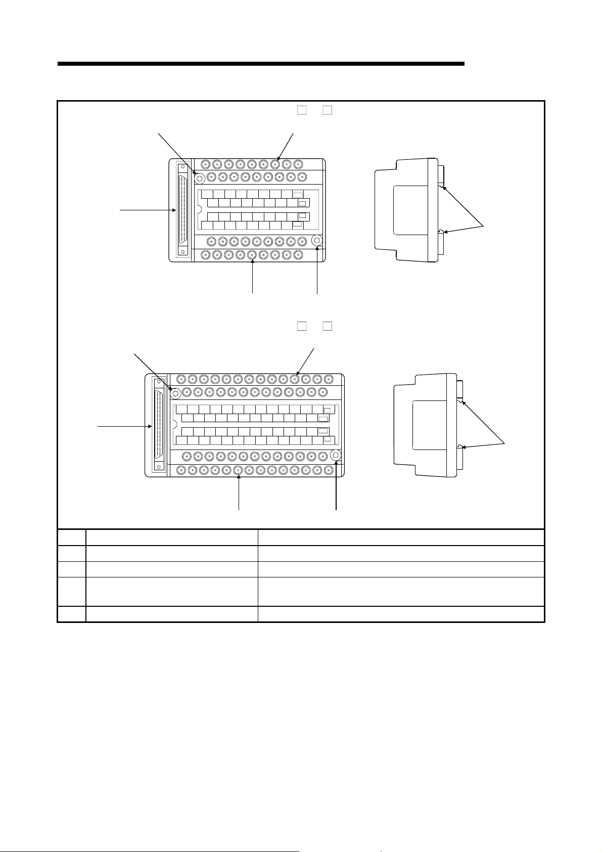
)
10 NAMES OF MODULE PARTS
1)
A6TB
2)
36
MELSEC-Q
02468ACE
3)
13579BDF
11 13 15 17 19 1B 1D 1F
10 12 14 16 18 1A1C1E
24V
0V
0V
24V
1)2)
4
1)
COM
0
3)
1
11
COM
10
COM COM COM COM
24 68 AC E
COM
COM
COM COM COM
35 79 BD F
COM COM COM
13 15 17 19 1B 1D 1F
COM COM COM COM
12 14 16 18 1A 1C 1E
A6TB 54
2)
0V
24V
24V
0V
4)
1)2)
No. Name Description
Panel mounting hole
1)
Terminal block
2)
40-pin connector
3)
Module fixing hook
4)
Used for mounting to panel (for M4 screw).
Used to connect power and signal wires.
Designed for 32-point module and used to connect power and
I/O signal wires.
Used for mounting onto DIN rail.
10 - 3 10 - 3
Page 77

10 NAMES OF MODULE PARTS
1)
A6TBX70
MELSEC-Q
2)
+C +C +C +C +C +C +C -C +C-C-C-C-C-C-C-C
+C
)
0123456789ABCDEF
10 11 12 13 14 151617 18 19 1A 1B 1C 1D1E1F
+C
+C +C +C +C +C +C +C -C +C-C-C-C-C-C-C-C
0V
24V
24V
0V
1)2)
No. Name Description
Panel mounting hole
1)
Terminal block
2)
40-pin connector
3)
Module fixing hook
4)
Used for mounting to panel (for M4 screw).
Used to connect power and signal wires.
Designed for 32-point module and used to connect power and
I/O signal wires.
Used for mounting onto DIN rail.
Q6TE
-18S
2
4
6
8
10
12
14
16
18
Q6TE-18S
1)
2)
1
3)
3
5
7
9
11
13
15
17
4)
No. Name Description
Terminal block mounting screw
1)
Circular shaped hole
2)
This is for securing Q6TE-18S terminal block to a module
A hole for inserting wire when wiring
3) Square shaped hole A hole for inserting a tool when wiring
10 - 4 10 - 4
Page 78

11 I/O MODULE TROUBLESHOOTING
MELSEC-Q
11. I/O MODULE TROUBLESHOOTING
This chapter explains possible problems with I/O circuits and their corrective actions.
11.1 Input Circuit Troubleshooting
This section describes possible problems with input circuits and their corrective
actions.
Condition Cause Corrective Action
Input signal
does not
turn OFF.
Example 1
Input signal
does not
turn OFF.
Example 2
Table 11.1 Input Circuit Problems and Corrective Actions
• Leakage current of input switch
(e.g. drive by non-contact switch).
AC input
Leakage
current
Power supply
• Drive by a limit switch w ith neon lamp.
Leakage
current
Input module
AC input
Input module
• Connect an appropriate resistor which will
make the voltage across the terminals of the
input module lower than the OFF voltage
value.
It is recommended to use 0.1 to 47 F + 47 to
120
• Same as Example 1.
• Or make up another independent display
circuit.
AC input
Input module
(1/2W) for the CR constant.
11
Input signal
does not
turn OFF.
Example 3
Power suppiy
• Leakage current due to line capacity of wiring
cable.
(Line capacity C of twisted pair wire is approx .
100 PF/m).
AC input
Leakage
current
Power supply
Input module
• Same as Example 1.
• However, leakage current is not generated
when the power supply is located in the input
equipment side as shown below.
Power supply
AC input
Input module
11 - 1 11 - 1
Page 79

)
pag
11
11 I/O MODULE TROUBLESHOOTING
Condition Cause Corrective Action
Input signal
does not
turn OFF.
Table 11.1 Input Circuit Problems and Corrective Actions (Continued)
• Drive by switch w ith LED indicator.
DC input
(Positive common
Leakage
current
Input module
• Connect a register which will make the voltage
between the input module terminal and
common lower than the OFF voltage, as
shown below.
Example 4
Resistor
MELSEC-Q
DC input
(Positive common)
Input module
A calculation example of a value for a
Input signal
does not
turn OFF.
Example 5
False input
due to
noise
• Sneak path due to the use of two power
supplies.
1
E
Depending on response time setting, noise is
imported as input.
E1E
>
2
E
2
Input module
Example 6
connected resistor is given on the following
e.
• Use only one power supply.
• Connect a sneak path prevention diode.
(Figure below)
2
E
E
1
Change response time setting.
Example
5ms
1ms
(Setting of a shorter response time may produce
a higher effect on periodic excessive noise.) If
no effects are produced by the above, take
basic actions to prevent excessive noise from
entering, e.g. avoid bundling the power and I/O
cables, and suppress noise by adding surge
absorbers to such noise sources as relays and
contactors used with the same power supply.)
Input module
<Calculation example of Example 4>
Consider a switch with LED indicator connected to the QX40, giving a leakage current
of 4mA when a 24VDC power is turned on.
QX40
3.6K
Leakage
current 4mA
24VDC
Input module
11 - 2 11 - 2
Page 80

11 I/O MODULE TROUBLESHOOTING
(1) The 1.7mA OFF current of the QX40 is not satisfied. Hence, connect a resistor as
shown below.
3.6K
R=
I
4mA
2.3mA
24VDC
(2) Calculate the resistor value R as indicated below.
To satisfy the 1.7mA OFF current of the QX40, the resistor R to be connected may
be the one where 2.3mA or more will flow.
I
: IZ=Z (Input impedance): R
R
QX40
Iz=1.7mA
Input impedance
5.6K
MELSEC-Q
I
Z
R Z (Input impedance) = 5.6=4.14[k ]
I
R
R<4.14k
Assuming that resistor R is 3.9k
W = (input voltage)
.
2
÷ R = 28.82 ÷ 3900 = 0.2(W)
1.7
2.3
, the power capacity W of resistor R is:
(3) The power capacity of the resistor selected is 3 to 5 times greater than the actual
current consumption. A 3.9 (k
), 0.6 to 1.0 (W) resistor may therefore be
connected to the terminal in question.
11 - 3 11 - 3
Page 81

11 I/O MODULE TROUBLESHOOTING
MELSEC-Q
11.2 Output Circuit Troubleshooting
This section describes possible problems with output circuits and their corrective
actions.
Condition Cause Corrective Action
When the
output is
OFF,
excessive
voltage is
applied to
the load.
Example 1
The load
does not
turn OFF
(triac
output).
Example 2
Table 11.2 output Circuit Problems and Corrective Actions
• Load is half-wave rectified inside (in some
cases, this is true of a solenoid).
QY22
Output module
• When the polarity of the power supply is as
shown in [1], C is charged. When the polarity is
as shown in [2], the voltage charged in C plus
the line voltage are applied across D1. Max.
voltage is approx. 2.2E.
(If a resistor is used in this way, it does not
pose a problem to the output element. But it
may cause the diode, which is built into the
load, to deteriorate, resulting in a fire, etc.)
• Leakage current due to built-in noise
suppression.
QY22
Output module
D1
Load
Load
Leakage current
[1]
[2]
• Connect a resistor several tens to hundreds of
across the load.
k
• Connect C and R across the load.
(When the wiring distance from the output card
to the load is long, there may be a leakage
current due to the line capacity.)
Resistor
Load
Resistor
Load
11 - 4 11 - 4
Page 82

APPENDICES
MELSEC-Q
APPENDICES
Appendix 1 External Di mensional D r awings
Appendix 1.1 I/O modules
(1) Terminal block connector type
(0.08) 90 (3.55)
(a) Other than QY22
(b) QY22 TRIAC Output Module
APP.
2
(0.08)
QX10
01234567
89ABCDEF
0
0
1
2
1
3
2
4
3
5
4
6
5
7
6
98 (3.86)
105 (4.14)
5
(0.2)
9
B
D
F
COM
100VAC
8mA60Hz
7mA50Hz
8
7
A
8
9
C
A
B
E
C
D
NC
E
F
27.4 (1.08)
2
(0.08)
QY22
01234567
89ABCDEF
FUSE
0
L
0
1
L
1
2
L
3
2
L
4
L
3
5
L
4
6
L
5
7
L
6
8
98 (3.86)
105 (4.14)
5
2 (0.08)
112.3 (4.42)
(0.2)
L
9
L
A
L
B
L
C
L
D
L
E
L
F
L
COM
100VAC
240VAC
0.6A
27.4 (1.08)
7
8
9
A
B
C
D
E
F
Unit: mm (inch)
App - 1 App - 1
Page 83

APP.
APPENDICES
(2) 40-pin connector type
(a) 32-point I/O module
MELSEC-Q
2
(0.08)
QX41
01234567
89ABCDEF
01234567
89ABCDEF
24VDC
4mA
QX41
98 (3.86)
105 (4.14)
2 (0.08)
90 (3.55)
5
(0.2)
45 (1.77)
27.4 (1.08)
(b) 64-point I/O module
2
(0.08)
QX42
01234567
89ABCDEF
01234567
89ABCDEF
24VDC
F L
4mA
QX42
DISPLAY
98 (3.86)
105 (4.14)
5
(0.2)
45 (1.77)
27.4 (1.08)2 (0.08) 90 (3.55)
Unit: mm (inch)
App - 2 App - 2
Page 84

APPENDICES
(3) 37-pin D-sub connector type 32- poi nt I/O modul e
2
(0.08)
98 (3.86)
105 (4.14)
MELSEC-Q
QX81
01234567
89ABCDEF
01234567
89ABCDEF
24VDC
4mA
QX81
5
2 (0.08)
90 (3.55)
(0.2)
46 (1.81)
27.4 (1.08)
(4) Blank cover module
2 (0.08)
QG60
QG60
100 (3.94)
98 (3.86)
2 (0.08)
90 (3.55)
27.4 (1.08)
Unit: mm (inch)
App - 3 App - 3
Page 85

)
)
APPENDICES
Appendix 1.2 Connectors, connector/terminal bl ock conv er ter modules
(1) 40-pin connectors
(a) A6CON1 soldering type, A6CON2 crimp-contact type 40-pin
connector
14 (0.55) or less
46 (1.81)
MELSEC-Q
72.72 (2.87)
(b) A6CON3 pressure-displacement type 40-pin connector
69.48 (2.74)
8.25 (0.3 3
22.5 (0.89
10 (0.39)
Flat cable
arrangement is in the
following sequence.
A1
B1 A2…
Unit: mm (inch)
App - 4 App - 4
Page 86

APPENDICES
MELSEC-Q
(2) 37-pin D-sub connectors
(a) A6CON1E soldering type, A6CON2E crimp-contact type 37-pin
D-sub connector
20.3
(0.8)
46 (1.81)
69.5 (2.74)
(b) A6CON3E pressure-displacement type 37-pin D-sub connector
12.6 (0.5)
69.4 (2.73)
3.4 (0.13)
5.9 (0.23)
Unit: mm (inch)
App - 5 App - 5
Page 87

APPENDICES
MELSEC-Q
(3) A6TB 36 connector/terminal block converter module
2 (0.08)- 4.5 (0.18) mounting hole
(M4 25)
44 (1.73)
78.5 (3.09)
17.3
(0.68)
89.6 (3.53)
120 (4.73)
5.5 (0.22)
48 (1.89)
52 (2.05)
(4) A6TB 54 connector/terminal block converter module
2 (0.08)- 4.5 (0.18) mounting hole
(M4 25)
44 (1.73)
78.5 (3.09)
17.3
(0.68)
124.6 (4.91)
155 (6.11)
5.5 (0.22)
48 (1.89)
52 (2.05)
(5) A6TBX70 connector/terminal block converter module
2 (0.08)- 4.5 (0.18) mounting hole
(M4 25)
190 (7.49)
159.6 (6.29)
44 (1.73)
17.3
(0.68)
5.5 (0.22)
78.5 (3.09)
48 (1.89)
52 (2.05)
Unit: mm (inch)
App - 6 App - 6
Page 88

APPENDICES
Appendix 1.3 Spring Clamp Terminal Block
MELSEC-Q
(1) Q6TE-18S Installed on a module (Ex ampl e: QX 10)
Q6TE
-18S
1
2
3
4
5
6
7
8
9
10
11
82.5 (3.25)
*: The depth of the module installed with a Q6TE-18S is equivalent with the factory default dimensions for that
module.
12
13
14
15
16
17
18
7.62 (0.30)
27
(1.06)
23
(0.91)
90*
(3.54)
Unit: mm(inch)
App - 7 App - 7
Page 89

APPENDICES
Appendix 2 Compatibility with MELSEC-AnS Series I/O modules
Note that the MELSEC-Q series I/O modules and MELSEC-AnS series I/O modules
are different in external terminal block configuration.
Differences in terminal block configuration are indicated below.
(1) Input modules
Terminal Block
Number
TB9 X08 X08 COM
TB10 X09 X09 X08
TB11 X0A X0A X09
•
•
•
TB16 X0F X0F X0E
TB17 COM NC X0F
TB18 NC COM COM
TB19 — — Vacant
TB20 — — Vacant
(2) Output modules
Terminal
Block
Number
TB9 Y08 Y08 COM1 12/24VDC
TB10 Y09 Y09 Y08 COM1
TB11 Y0A Y0A Y09 Y08
•
•
•
TB16 Y0F Y0F Y0E Y0D
TB17 COM 12/24VDC Y0F Y0E
TB18 NC COM COM2 Y0F
TB19 — — 24VDC 12/24VDC
TB20 — — 0V COM2
QY10 QY40P A1SY10 A1SY40
•
•
•
QX10, QX40 QX80
•
•
•
•
•
•
•
•
•
MELSEC-Q
A1SX10, A1SX40,
A1SX80
•
•
•
•
•
•
•
•
•
App - 8 App - 8
Page 90

APPENDICES
MELSEC-Q
Terminal
Block
Number
TB9 Y08 12/24VDC TB9 Y08 COM1
TB10 Y09 COM1 TB10 Y09 0V
TB11 Y0A Y08 TB11 Y0A Y08
•
•
•
TB16 Y0F Y0D TB16 Y0F Y0D
TB17 12/24VDC Y0E TB17 COM Y0E
TB18 COM Y0F TB18 0V Y0F
TB19 — 12/24VDC TB19 — COM2
TB20 — COM2 TB20 — 0V
POINT
QY50 A1SY50
•
•
•
•
•
•
Terminal
Block
Number
•
•
•
QY80 A1SY80
•
•
•
The 40-pin connector used with the MELSEC-AnS series I/O module can be used
intact with the MELSEC-Q series I/O module.
The 37-pin D-sub connector used with the MELSEC-AnS series I/O module is the
same in wiring as, but opposite in cable pulling direction to, the MELSEC-Q series
I/O module. (The conventional cable for A6TB cannot be used.)
•
•
•
App - 9 App - 9
Page 91

WARRANTY
Please confirm the following product warranty details before starting use.
1. Gratis Warranty Term and Gratis Warranty Range
If any faults or defects (hereinafter "Failure") found to be the responsibility of Mitsubishi occurs during use of the product
within the gratis warranty term, the product shall be repaired at no cost via the dealer or M itsubishi Serv ice Company .
Note that if repairs are required at a site overseas, on a detached island or remote place, expenses to dispatch an
engineer shall be charged for.
[Gratis Warranty Term]
The gratis warranty term of the product shall be for one year after the date of purchase or delivery to a designated
place.
Note that after manufacture and shipment from Mitsubishi, the maximum distribution period shall be six (6) months, and
the longest gratis warranty term after manufacturing shall be eighteen (18) months. The gratis warranty term of repair
parts shall not exceed the gratis warranty term before repairs.
[Gratis Warranty Range]
(1) The range shall be limited to normal use within the usage state, usage methods and usage environment, etc.,
which follow the conditions and precautions, etc., given in the instruction manual, user's manual and caution labels
on the product.
(2) Even within the gratis warranty term, repairs shall be charged for in the follow ing cases.
1. Failure occurring from inappropriate storage or handling, carelessness or negligence by the user. Failure caused
by the user's hardware or software design.
2. Failure caused by unapproved modifications, etc., to the product by the user.
3. When the Mitsubishi product is assembled into a user's device, Failure that could have been avoided if functions
or structures, judged as necessary in the legal safety measures the user's device is subject to or as necessary
by industry standards, had been provided.
4. Failure that could have been avoided if consumable parts (battery, backlight, fuse, etc.) designated in the
instruction manual had been correctly serviced or replaced.
5. Failure caused by external irresistible forces such as fires or abnormal voltages, and Failure caused by force
majeure such as earthquakes, lightning, wind and water damage.
6. Failure caused by reasons unpredictable by scientific technology standards at time of shipment from Mitsubishi.
7. Any other failure found not to be the responsibility of Mitsubishi or the user.
2. Onerous repair term after discontinuation of production
(1) Mitsubishi shall accept onerous product repairs for seven (7) years after production of the product is discontinued.
Discontinuation of production shall be notified with Mitsubishi Technical Bulletins, etc.
(2) Product supply (including repair parts) is not possible after production is discontinued.
3. Overseas service
Overseas, repairs shall be accepted by Mitsubishi's local overseas FA C enter. Note that the repair conditions at each FA
Center may differ.
4. Exclusion of chance loss and secondary loss from warranty liability
Regardless of the gratis warranty term, Mitsubishi shall not be liable for compensation to damages caused by any cause
found not to be the responsibility of Mitsubishi, chance losses, lost profits incurred to the user by Failures of Mitsubishi
products, damages and secondary damages caused from special reasons regardless of Mitsubishi's expectations,
compensation for accidents, and compensation for damages to products other than Mitsubishi products and other duties.
5. Changes in product specifications
The specifications given in the catalogs, manuals or technical documents are subject to change without prior notice.
6. Product application
(1) In using the Mitsubishi MELSEC programmable logic controller, the usage conditions shall be that the application w ill
not lead to a major accident even if any problem or fault should occur in the programmable logic controller device, and
that backup and fail-safe functions are systematically provided outside of the device for any problem or fault.
(2) The Mitsubishi general-purpose programmable logic controller has been designed and manufactured for applications
in general industries, etc. Thus, applications in which the public could be affected such as in nuclear power plants and
other power plants operated by respective power companies, and applications in w hich a special quality assurance
system is required, such as for Railway companies or National Defense purposes shall be ex cluded from the
programmable logic controller applications.
Note that even with these applications, if the user approves that the application is to be limited and a special quality is
not required, application shall be possible.
When considering use in aircraft, medical applications, railways, incineration and fuel devices, manned transport
devices, equipment for recreation and amusement, and safety devices, in which human life or assets could be greatly
affected and for which a particularly high reliability is required in terms of safety and control system, please consult
with Mitsubishi and discuss the required specifications.
Page 92

MIT
SUBIS
C
C
HI ELECTRI
HEADQUARTERS
MITSUBISHI ELECTRIC EUROPE
EUROPE B.V.
German Branch
Gothaer Straße 8
D-40880 Ratingen
Phone: +49 (0) 2102 / 486-0
Fax: +49 (0) 2102 / 486-1120
e mail: megfamail@meg.mee.com
MITSUBISHI ELECTRIC FRANCE
EUROPE B.V.
French Branch
25, Boulevard des Bouvets
F-92741 Nanterre Cedex
Phone:+33155685568
Fax:+33155685685
e mai l : factory.automation@fra.mee.com
MITSUBISHI ELECTRIC IRELAND
EUROPE B.V.
Irish Branch
Westgate Business Park, Ballymount
IRL-Dublin 24
Phone: +353 (0) 1 / 419 88 00
Fax: +353 (0) 1 / 419 88 90
e mail: sales.info@meir.mee.com
MITSUBISHI ELECTRIC ITALY
EUROPE B.V.
Italian Branch
Via Paracelso 12
I-20041 Agrate Brianza (MI)
Phone: +39 039 6053 1
Fax: +39 039 6053 312
e mail: factory.automation@it.mee.com
MITSUBISHI ELECTRIC SPAIN
EUROPE B.V.
Spanish Branch
Carretera de Rubí 76-80
E-08190 Sant Cugat del Vallés
Phone:+3493/5653131
Fax:+3493/5892948
e mail: industrial@sp.mee.com
MITSUBISHI ELECTRIC UK
EUROPE B.V.
UK Branch
Travellers Lane
GB-HatfieldHerts.AL108XB
Phone: +44 (0) 1707 / 27 61 00
Fax: +44 (0) 1707 / 27 86 95
e mail: automation@meuk.mee.com
MITSUBISHI ELECTRIC JAPAN
CORPORATION
Office Tower “Z” 14 F
8-12,1 chome, Harumi Chuo-Ku
Tokyo 104-6212
Phone: +81 3 6221 6060
Fax: +81 3 6221 6075
MITSUBISHI ELECTRIC USA
AUTOMATION
500 Corporate Woods Parkway
Vernon Hills, IL 60061
Phone: +1 847 / 478 21 00
Fax: +1 847 / 478 22 83
MIDDLE EAST REPRESENTATIVE
TEXEL Electronics Ltd. ISRAEL
Box 6272
IL-42160 Netanya
Phone: +972 (0) 9 / 863 08 91
Fax: +972 (0) 9 / 885 24 30
e mail: texel_me@netvision.net.il
EUROPEAN REPRESENTATIVES
GEVA AUSTRIA
Wiener Straße 89
AT-2500 Baden
Phone: +43 (0) 2252 / 85 55 20
Fax: +43 (0) 2252 / 488 60
e mail: office@geva.at
TEHNIKON BELARUS
Oktjabrskaya 16/5, Ap 704
BY-220030 Minsk
Phone: +375 (0)17 / 22 75 704
Fax: +375 (0)17 / 22 76 669
e mail: tehnikon@belsonet.net
Getronics b.v. BELGIUM
Control Systems
Pontbeeklaan 43
B-1731 Asse-Zellik
Phone: +32 (0) 2 / 467 17 51
Fax: +32 (0) 2 / 467 17 45
e mail: infoautomation@getronics.com
TELECON CO. BULGARIA
4, A. Ljapchev Blvd.
BG-1756 Sofia
Phone:+359(0)2/9744058
Fax:+359(0)2/9744061
e mail: —
INEA CR d.o.o. CROATIA
Drvinje 63
HR-10000 Zagreb
Phone: +385 (0) 1 / 36 67 140
Fax: +385 (0) 1 / 36 67 140
e mail: —
AutoCont CZECH REPUBLIC
Control Systems s.r.o.
Nemocnicni 12
CZ-702 00 Ostrava 2
Phone: +420 59 / 6152 111
Fax: +420 59 / 6152 562
e mail: consys@autocont.cz
louis poulsen DENMARK
industri & automation
Geminivej 32
DK-2670 Greve
Phone:+45(0)70/101535
Fax:+45(0)43/959591
e mail: lpia@lpmail.com
UTU Elektrotehnika AS ESTONIA
Pärnu mnt.160i
EE-11317 Tallinn
Phone:+372(0)6/517280
Fax:+372(0)6/517288
e mail: utu@utu.ee
Beijer Electronics OY FINLAND
Ansatie 6a
FIN-01740 Vantaa
Phone: +358 (0) 9 / 886 77 500
Fax: +358 (0) 9 / 886 77 555
e mail: info@beijer.fi
UTECO A.B.E.E. GREECE
5, Mavrogenous Str.
GR-18542 Piraeus
Phone: +302 (0) 10 / 42 10 050
Fax: +302 (0) 10 / 42 12 033
e mail: sales@uteco.gr
Meltrade Automatika Kft. HUNGARY
55, Harmat St.
HU-1105 Budapest
Phone: +36 (0)1 / 2605 602
Fax: +36 (0)1 / 2605 602
e mail: office@meltrade.hu
SIA POWEL LATVIA
Lienes iela 28
LV-1009 Riga
Phone: +371 784 / 22 80
Fax: +371 784 / 22 81
e mail: utu@utu.lv
EUROPEAN REPRESENTATIVES
UAB UTU POWEL LITHUANIA
Savanoriu pr. 187
LT-2053 Vilnius
Phone: +370 (0) 52323-101
Fax: +370 (0) 52322-980
e mail: powel@utu.lt
INTEHSIS SRL MOLDOVA
Cuza-Voda 36/1-81
MD-2061 Chisinau
Phone: +373 (0)2 / 562 263
Fax: +373 (0)2 / 562 263
e mail: intehsis@mdl.net
Getronics b.v. NETHERLANDS
Control Systems
Donauweg 2 B
NL-1043 AJ Amsterdam
Phone: +31 (0) 20 / 587 67 00
Fax: +31 (0) 20 / 587 68 39
e mail: info.gia@getronics.com
Beijer Electronics AS NORWAY
Teglverksveien 1
N-3002 Drammen
Phone:+47(0)32/243000
Fax:+47(0)32/848577
e mail: info@beijer.no
MPL Technology Sp. z o.o. POLAND
ul. Sliczna 36
PL-31-444 Kraków
Phone: +48 (0) 12 / 632 28 85
Fax: +48 (0) 12 / 632 47 82
e mail: krakow@mpl.pl
Sirius Trading & Services srl ROMANIA
Str. Biharia No. 67-77
RO-013981 Bucuresti 1
Phone: +40 (0) 21 / 201 1146
Fax: +40 (0) 21 / 201 1148
e mail: sirius@siriustrading.ro
INEA d.o.o. SLOVENIA
Stegne 11
SI-1000 Ljubljana
Phone: +386 (0) 1-513 8100
Fax: +386 (0) 1-513 8170
e mail: inea@inea.si
Beijer Electronics AB SWEDEN
Box 426
S-20124 Malmö
Phone:+46(0)40/358600
Fax:+46(0)40/358602
e mail: info@beijer.se
ECONOTEC AG SWITZERLAND
Postfach 282
CH-8309 Nürensdorf
Phone: +41 (0) 1 / 838 48 11
Fax: +41 (0) 1 / 838 48 12
e mail: info@econotec.ch
GTS TURKEY
Darülaceze Cad. No. 43 Kat. 2
TR-80270 Okmeydani-Istanbul
Phone: +90 (0) 212 / 320 1640
Fax: +90 (0) 212 / 320 1649
e mail: gts@turk.net
CSC Automation Ltd. UKRAINE
15, M. Raskova St., Fl. 10, Office 1010
UA-02002 Kiev
Phone: +380 (0) 44 / 238-83-16
Fax: +380 (0) 44 / 238-83-17
e mail: csc-a@csc-a.kiev.ua
EUROPEAN REPRESENTATIVES
Avtomatika Sever Ltd. RUSSIA
Lva Tolstogo St. 7, Off. 311
RU-197376 St Petersburg
Phone: +7 812 / 11 83 238
Fax: +7 812 / 11 83 239
e mail: as@avtsev.spb.ru
CONSYS RUSSIA
Promyshlennaya St. 42
RU-198099 St Petersburg
Phone: +7 812 / 325 36 53
Fax: +7 812 / 147 20 55
e mail: consys@consys.spb.ru
Electrotechnical RUSSIA
Systems Siberia
Partizanskaya St. 27, Office 306
RU-121355 Moscow
Phone: +7 095/ 416-4321
Fax: +7 095/ 416-4321
e mail: info@eltechsystems.ru
Electrotechnical RUSSIA
Systems Siberia
Shetinkina St. 33, Office 116
RU-630088 Novosibirsk
Phone: +7 3832 / 22-03-05
Fax: +7 3832 / 22-03-05
e mail: info@eltechsystems.ru
Elektrostyle RUSSIA
ul. Garschina 11
RU-140070 Moscow
Phone: +7 095 / 514 9316
Fax: +7 095 / 514 9317
e mail: info@estl.ru
Elektrostyle RUSSIA
Krasnij Prospekt 220-1
Office No. 312
RU-630049 Novosibirsk
Phone: +7 3832 / 10 66 18
Fax: +7 3832 / 10 66 26
e mail: info@estl.ru
ICOS RUSSIA
Industrial Computer Systems Zao
Ryazanskij Prospekt 8a, Office 100
RU-109428 Moscow
Phone: +7 095 / 232 - 0207
Fax: +7 095 / 232 - 0327
e mail: mail@icos.ru
NPP Uralelektra RUSSIA
ul. Sverdlova 11a
RU-620027 Ekaterinburg
Phone: +7 34 32 / 53 27 45
Fax: +7 34 32 / 53 27 45
e mail: elektra@etel.ru
SSMP Rosgidromontazh Ltd. RUSSIA
23, Lesoparkovaya Str.
RU-344041 Rostov On Don
Phone: +7 8632 / 36 00 22
Fax: +7 8632 / 36 00 26
e mail: —
STC Drive Technique RUSSIA
ul. Bajkalskaja 239, Office 2 - 23
RU-664075 Irkutsk
Phone: +7 3952 / 24 38 16
Fax: +7 3952 / 23 02 98
e mail: privod@irk.ru
STC Drive Technique RUSSIA
PoslannikovPer.9,str.1
RU-107005 Moscow
Phone: +7 095 / 790-72-10
Fax: +7 095 / 790-72-12
e mail: info@privod.ru
AFRICAN REPRESENTATIVE
CBI Ltd. SOUTH AFRICA
Private Bag 2016
ZA-1600 Isando
Phone: +27 (0) 11/ 928 2000
Fax: +27 (0) 11/ 392 2354
e mail: cbi@cbi.co.za
MITSUBISHI ELECTRI
Gothaer Strasse 8 Phone: +49 2102 486-0 Fax: +49 2102 486-7170 www.mitsubishi-automation.de
D-40880 Ratingen Hotline: +49 1805 000-765 megfa-mail@meg.mee.com www.mitsubishi-automation.com
INDUSTRIAL AUTOMATION
 Loading...