

MITSUBISHI PM600CLA060 Technical data
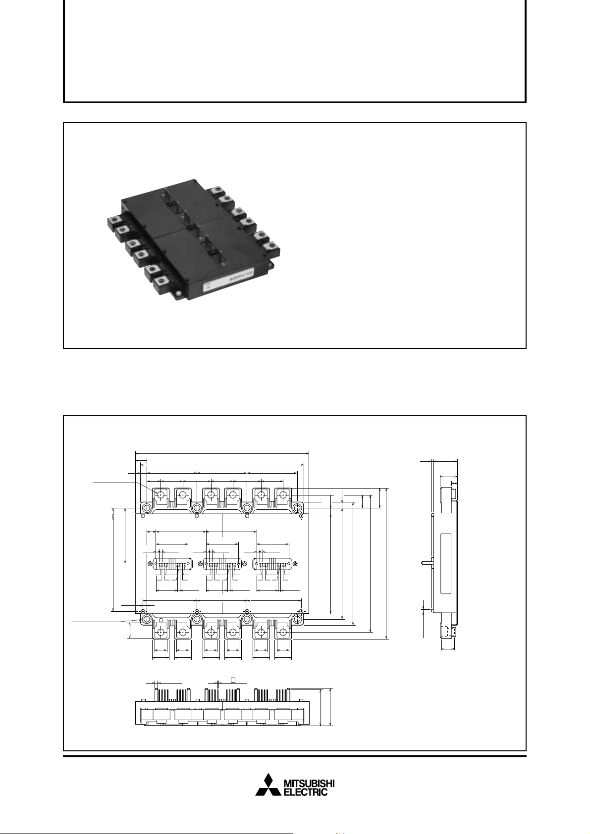
PM600CLA060
MITSUBISHI <INTELLIGENT POWER MODULES>
PM600CLA060
FLA T-BASE TYPE
INSULATED PACKAGE
FEATURE
a) Adopting new 5th generation IGBT (CSTBT) chip, which
performance is improved by 1µm fine rule process.
For example, typical V
b) I adopt the over-temperature conservation by Tj detection of
CSTBT chip, and error output is possible from all each conservation upper and lower arm of IPM.
•3φ 600A, 600V Current-sense IGBT type inverter
• Monolithic gate drive & protection logic
• Detection, protection & status indication circuits for, shortcircuit, over-temperature & under-voltage (Fo available from
all arm devices)
• Acoustic noise-less 45kW/55kW class inverter application
• UL Recognized Yellow Card No.E80276(N)
ce(sat)=1.8V @Tj=125°C
File No.E80271
APPLICATION
General purpose inverter, servo drives and other motor controls
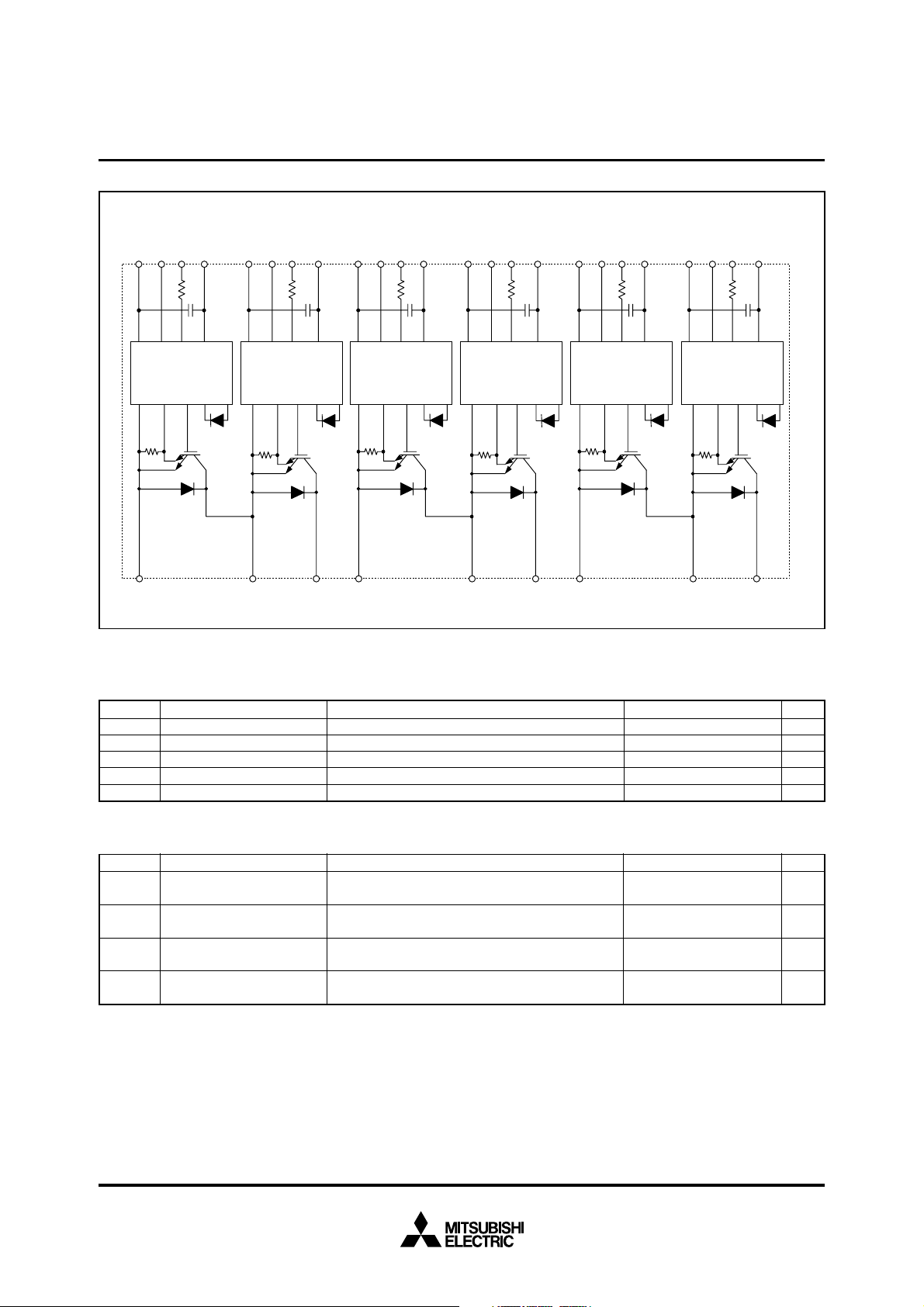
PACKAGE OUTLINES Dimensions in mm
172
162
50±
0.5
50
31.84
3-2.543.22
21222423252628
21 3-2.54
12
171217
24- 0.64
27
50±
0.5
31.84
3-2.543.22
29303231333436
21 3-2.54
12
171217
(24)2
+1.0
17
–0.5
6
6.5
5.5
0.5
99
35
110±
123
13.5
137
20
150
LABEL
8-φ3.5
12
(SCREWING DEPTH)
Terminal code
1. N
7. W
35.5
36.6
2. P
3. N
4. P
5. N
6. P
8. W
9. V
10. V
11. U
12. U
13. VUPC
14. UPFO
15. UP
16. VUP1
17. VUNC
18. UNFO
19. UN
20. VUN1
21. VVPC
22. VPFO
23. VP
24. VVP1
25. VVNC
26. VNFO
27. VN
28. VVN1
29. VWPC
30. WPFO
31. WP
32. VWP1
33. VWNC
34. WNFO
35. WN
36. VWN1
12-M6 NUTS
7.75
94.5
8-φ5.5
MOUNTING HOLES
11
50±
6
55
3.75
(15.5)
0.5
14 22 28 22 2228
121110987
9.08
50
31.84
3-2.543.22
13141615171820
19
21 3-2.54
53.75 50 53.75
12 34 56
12
171217
6-φ2.5
Jul. 2005
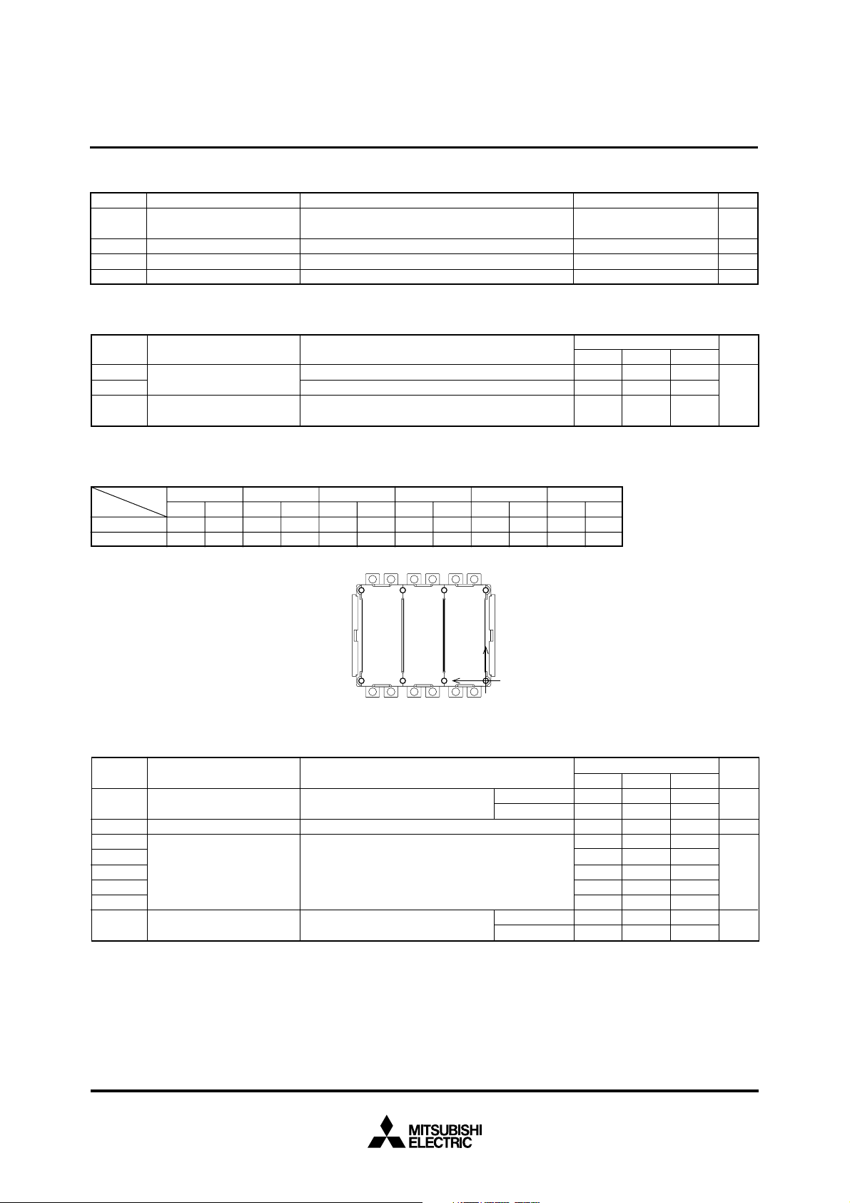
INTERNAL FUNCTIONS BLOCK DIAGRAM
WN V
WNC
NFO
1.5k 1.5k 1.5k 1.5k1.5k 1.5k
V
WN1
W
V
WPC
WP V
W
PFO
WP1
V
VNC
VN V
V
NFO
VN1
V
VPC
MITSUBISHI <INTELLIGENT POWER MODULES>
PM600CLA060
FLA T-BASE TYPE
INSULATED PACKAGE
UN V
VP V
V
PFO
VP1
UNC
NFO
V
UN1
U
V
UPC
UP V
U
PFO
UP1
Gnd In Fo Vcc
Gnd Si Out OT
NWP
Gnd In Fo Vcc
Gnd Si Out OT
Gnd In Fo Vcc
Gnd Si Out OT
NVP
Gnd In Fo Vcc
Gnd Si Out OT
Gnd In Fo Vcc
Gnd Si Out OT
NUP
Gnd In Fo Vcc
Gnd Si Out OT
MAXIMUM RATINGS (Tj = 25°C, unless otherwise noted)
INVERTER PART
Symbol Parameter Condition Ratings Unit
VCES
±IC
±ICP
PC
Tj
Collector-Emitter Voltage
Collector Current
Collector Current (Peak)
Collector Dissipation
Junction Temperature
V
D = 15V, VCIN = 15V
T
C = 25°C
T
C = 25°C
T
C = 25°C (Note-1)
600
600
1200
1785
–20 ~ +150
V
A
A
W
°C
CONTROL PART
Symbol Parameter Condition Ratings Unit
VD
VCIN
VFO
IFO
Supply Voltage
Input Voltage
Fault Output Supply Voltage
Fault Output Current
Applied between : V
Applied between : UP-VUPC, VP-VVPC, WP-VWPC
Applied between : UPFO-VUPC, VPFO-VVPC, WPFO-VWPC
Sink current at UPFO, VPFO, WPFO, UNFO, VNFO, WNFO
terminals
UP1-VUPC, VVP1-VVPC, VWP1-VWPC
VUN1-VUNC, VVN1-VVNC, VWN1-VWNC
UN-VUNC, VN-VVNC, WN-VWNC
UNFO-VUNC, VNFO-VVNC, WNFO-VWNC
20
20
20
20
Jul. 2005
V
V
V
mA
TOTAL SYSTEM
Symbol
V
CC(PROT)
V
CC(surge)
Tstg
Viso
Supply Voltage Protected by
SC
Supply Voltage (Surge)
Storage Temperature
Isolation Voltage
Parameter
V
D = 13.5 ~ 16.5V, Inverter Part,
j = +125°C Start
T
Applied between : P-N, Surge value
60Hz, Sinusoidal, Charged part to Base, AC 1 min.
THERMAL RESISTANCES
Symbol
Rth(j-c)Q
Rth(j-c)F
Rth(c-f)
Junction to case Thermal
Resistances
Contact Thermal Resistance
(Note-1) Tc measurement point is just under the chip.
If you use this value, R
Table 1: Tc (under the chip) measurement point is below.
arm
axis
X
Y
IGBT
30.5
82.8
Parameter
UP
FWDi
20.4
82.8
Inverter IGBT (per 1 element) (Note-1)
Inverter FWDi (per 1 element) (Note-1)
Case to fin, (per 1 module)
Thermal grease applied (Note-1)
th(f-a) should be measured just under the chips.
VP WP UN VN WN
IGBT
FWDi
IGBT
80.5
70.4
130.5
82.8
82.8
82.8
FWDi
120.4
82.8
Condition
Condition
IGBT
19.4
27.2
MITSUBISHI <INTELLIGENT POWER MODULES>
PM600CLA060
FLA T-BASE TYPE
INSULATED PACKAGE
Ratings
400
500
–40 ~ +125
2500
Limits
FWDi
29.6
27.2
IGBT
69.4
27.2
FWDi
79.6
27.2
(Unit : mm)
IGBT
119.4
27.2
Min.
—
—
—
FWDi
129.6
27.2
Typ. Max.
0.07
—
0.11
—
0.014
—
Unit
V
V
°C
V
rms
Unit
°C/W
Name
plate
side
7
Bottom
view
13
X
ELECTRICAL CHARACTERISTICS (Tj = 25°C, unless otherwise noted)
INVERTER PART
= 15V
Condition
(Fig. 5)
Symbol
CE(sat)
V
VEC
ton
trr
tc(on)
toff
tc(off)
ICES
Parameter
Collector-Emitter
Saturation Voltage
FWDi Forward Voltage
Switching Time
Collector-Emitter
Cutoff Current
D = 15V, IC = 600A
V
V
CIN = 0V (Fig. 1)
–I
C = 600A, VD = 15V, VCIN = 15V (Fig. 2)
D = 15V, VCIN = 0V↔15V
V
V
CC = 300V, IC = 600A
T
j = 125°C
Inductive Load (Fig. 3, 4)
VCE = V
CES
, V
CIN
Y
16
T
j = 25°C
T
j = 125°C
T
j = 25°C
T
j = 125°C
Limits
Min. Typ. Max.
—
—
—
0.5
—
—
—
—
—
—
1.7
1.8
2.6
1.0
0.2
0.4
2.2
0.6
—
—
2.2
2.3
3.7
2.4
0.4
1.0
3.5
1.1
10
Unit
V
V
µs
1
mA
Jul. 2005
 Loading...