

MITSUBISHI <INTELLIGENT POWER MODULES>
■
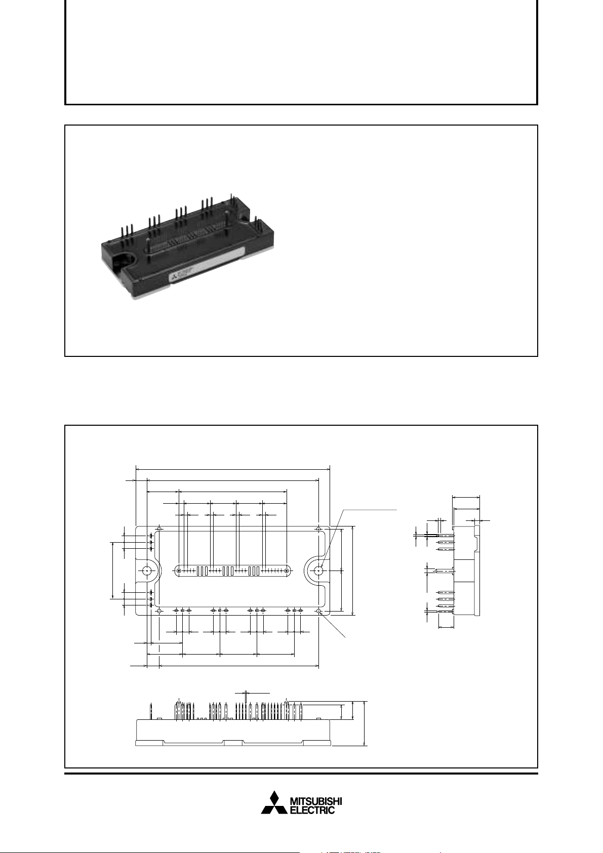
PM50CLB060
FLAT-BASE TYPE
INSULATED PACKAGE
PM50CLB060
FEATURE
a) Adopting new 5th generation IGBT (CSTBT) chip, which
performance is improved by 1µm fine rule process.
For example, typical V
b) I adopt the over-temperature conservation by Tj detection of
CSTBT chip, and error output is possible from all each conservation upper and lower arm of IPM.
c) New small package
Reduce the package size by 32%, thickness by 22% from
S-DASH series.
•3φ 50A, 600V Current-sense IGBT type inverter
• Monolithic gate drive & protection logic
• Detection, protection & status indication circuits for, shortcircuit, over-temperature & under-voltage (P-Fo available
from upper arm devices)
• Acoustic noise-less 3.7kW class inverter application
• UL Recognized Yellow Card No.E80276(N)
APPLICATION
General purpose inverter, servo drives and other motor controls
ce(sat)=1.5V @Tj=125°C
File No.E80271
PACKAGE OUTLINES Dimensions in mm
120
7
3.25
44
NP
35
44
2.5
7.75 98.25
15
BUVW
44444444
19.5
22
106
±0.25
66.519.75
16 15.25
1616
6-23-23-23-2
91319
0.5
19-
17
2-φ5.5
MOUNTING HOLES
25.7525
55
4-
φ2.5
232323
9.5
11.5
27.5
1.5
1
1.5
2-φ2.5
1
Terminal code
1. VUPC
2. UFO
3. UP
4. VUP1
5. VVPC
6. VFO
7. VP
8. VVP1
9. VWPC
10. WFO
16
3
9.5
11. WP
12. VWP1
13. VNC
14. VN1
15. NC
16. UN
17. VN
18. WN
19. Fo
May 2005
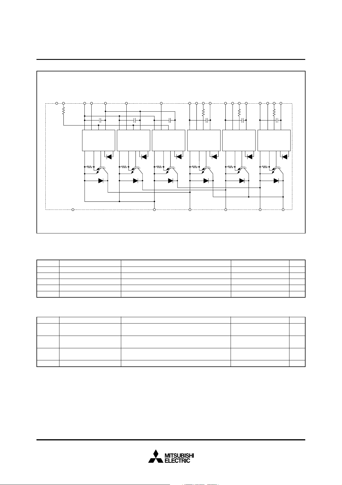
INTERNAL FUNCTIONS BLOCK DIAGRAM
V
NC
Fo
V
NC
V
N1
W
N
N
MITSUBISHI <INTELLIGENT POWER MODULES>
PM50CLB060
FLAT-BASE TYPE
INSULATED PACKAGE
WPV
U
N
V
WPC
WF
WP1
O
V
VPC
VPV
VF
VP1
O
V
UPC
UPV
UF
UP1
O
1.5k
Gnd In Fo Vcc
Gnd Si Out OT
NC N W V U P
Gnd In Fo Vcc
Gnd Si Out OT
Gnd In Fo Vcc
Gnd Si Out OT
1.5k 1.5k 1.5k
Gnd In Fo Vcc
Gnd Si Out OT
Gnd In Fo Vcc
Gnd Si Out OT
Gnd In Fo Vcc
Gnd Si Out OT
MAXIMUM RATINGS (Tj = 25°C, unless otherwise noted)
INVERTER PART
Symbol Parameter Condition Ratings Unit
VCES
±IC
±ICP
PC
Tj
Collector-Emitter Voltage
Collector Current
Collector Current (Peak)
Collector Dissipation
Junction Temperature
D = 15V, VCIN = 15V
V
C = 25°C
T
T
C = 25°C
C = 25°C (Note-1)
T
600
50
100
131
–20 ~ +150
V
A
A
W
°C
CONTROL PART
Symbol Parameter Condition Ratings Unit
VD
VCIN
VFO
IFO
Supply Voltage
Input Voltage
Fault Output Supply Voltage
Fault Output Current
Applied between : V
Applied between : UP-VUPC, VP-VVPC
Applied between : UFO-VUPC, VFO-VVPC, WFO-VWPC
Sink current at UFO, VFO, WFO, FO terminals
UP1-VUPC
VVP1-VVPC, VWP1-VWPC, VN1-VNC
WP-VWPC, UN • VN • WN-VNC
FO-VNC
20
20
20
20
May 2005
V
V
V
mA
TOTAL SYSTEM
ParameterSymbol
CC(PROT)
V
CC(surge)
V
Tstg
Viso
Supply Voltage Protected by
SC
Supply Voltage (Surge)
Storage Temperature
Isolation Voltage
V
D = 13.5 ~ 16.5V, Inverter Part,
T
j = +125°C Start
Applied between : P-N, Surge value
60Hz, Sinusoidal, Charged part to Base, AC 1 min.
THERMAL RESISTANCES
Symbol
Rth(j-c)Q
Rth(j-c)F
Rth(c-f)
Junction to case Thermal
Resistances
Contact Thermal Resistance
* If you use this value, R
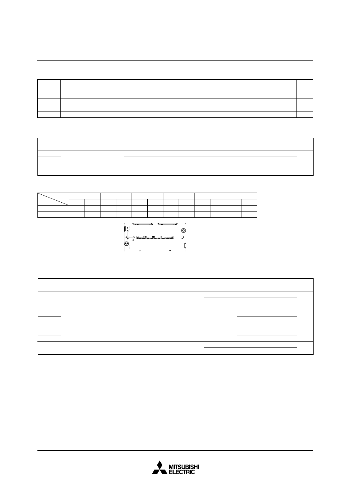
(Note-1) Tc (under the chip) measurement point is below.
arm
axis
X
Y
Parameter
Inverter IGBT (per 1 element) (Note-1)
Inverter FWDi (per 1 element) (Note-1)
Case to fin, (per 1 module)
Thermal grease applied (Note-1)
th(f-a) should be measured just under the chips.
IGBT
29.0
–7.3
UP
FWDi
29.5
1.6
VP WP UN VN WN
IGBT
FWDi
IGBT
64.6
65.1
85.9
–7.3
2.1
–7.3
FWDi
86.4
2.1
Condition
Condition
IGBT
38.1
5.3
MITSUBISHI <INTELLIGENT POWER MODULES>
PM50CLB060
FLAT-BASE TYPE
INSULATED PACKAGE
Ratings
400
500
–40 ~ +125
2500
Limits
FWDi
37.6
–4.6
IGBT
54.8
5.3
FWDi
55.3
–4.6
(unit : mm)
IGBT
76.1
5.3
Min.
—
—
—
FWDi
75.6
–4.6
Typ. Max.
0.95*
—
1.61*
—
0.038
—
Unit
V
V
°C
rms
V
Unit
°C/W
Bottom view
ELECTRICAL CHARACTERISTICS (Tj = 25°C, unless otherwise noted)
INVERTER PART
= 15V
Condition
(Fig. 5)
Symbol
V
CE(sat)
VEC
ton
trr
tc(on)
toff
tc(off)
ICES
Parameter
Collector-Emitter
Saturation Voltage
FWDi Forward Voltage
Switching Time
Collector-Emitter
Cutoff Current
D = 15V, IC = 50A
V
V
CIN = 0V (Fig. 1)
C = 50A, VD = 15V, VCIN = 15V (Fig. 2)
–I
D = 15V, VCIN = 0V↔15V
V
V
CC = 300V, IC = 50A
j = 125°C
T
Inductive Load (Fig. 3,4)
VCE = V
CES
, V
CIN
j = 25°C
T
j = 125°C
T
j = 25°C
T
j = 125°C
T
Limits
Min. Typ. Max.
—
—
—
0.5
—
—
—
—
—
—
1.6
1.5
2.2
1.0
0.2
0.4
1.2
0.5
—
—
2.1
2.0
3.3
2.4
0.4
1.0
2.5
1.0
10
Unit
V
V
µs
1
mA
May 2005

MITSUBISHI <INTELLIGENT POWER MODULES>
PM50CLB060
FLAT-BASE TYPE
INSULATED PACKAGE
CONTROL PART
—
—
1.2
1.7
100
—
135
—
—
—
—
1.0
Limits
15
1.5
2.0
—
0.2
145
125
12.0
12.5
—
10
1.8
25
10
1.8
2.3
—
—
—
—
—
15
—
Unit
mA
V
A
µs
°C
V
mA
ms
Max.
5
12.5
0.01
Symbol
ID
V
th(ON)
Vth(OFF)
SC
t
off(SC)
OT
OT
r
UV
UV
r
IFO(H)
IFO(L)
tFO
Circuit Current
Input ON Threshold Voltage
Input OFF Threshold Voltage
Short Circuit Trip Level
Short Circuit Current Delay
Time
Over Temperature Protection
Supply Circuit Under-Voltage
Protection
Fault Output Current
Minimum Fault Output Pulse
Width
Parameter
Condition
VD = 15V, VCIN = 15V
Applied between : U
P-VUPC, VP-VVPC, WP-VWPC
VN1-VNC
V*P1-V*PC
UN • VN • WN-VNC
j ≤ 125°C, VD = 15V (Fig. 3,6)
–20 ≤ T
V
D = 15V (Fig. 3,6)
V
D = 15V
Detect Tj of IGBT chip
–20 ≤ T
j ≤ 125°C
D = 15V, VFO = 15V (Note-2)
V
D = 15V (Note-2)
V
Trip level
Reset level
Trip level
Reset level
Min. Typ.
11. 5
(Note-2) Fault output is given only when the internal SC, OT & UV protections schemes of either upper or lower arm device operate to
protect it.
MECHANICAL RATINGS AND CHARACTERISTICS
Symbol
—
—
Parameter
Mounting torque
Weight
Mounting part screw : M5
Condition
—
Min.
2.5
—
RECOMMENDED CONDITIONS FOR USE
Symbol Parameter
VCC
VD
VCIN(ON)
VCIN(OFF)
fPWM
t
dead
Supply Voltage
Control Supply Voltage
Input ON Voltage
Input OFF Voltage
PWM Input Frequency
Arm Shoot-through
Blocking Time
Applied across P-N terminals
Applied between : V
Applied between : U
Using Application Circuit of Fig. 8
For IPM’s each input signals (Fig. 7) ≥ 2.0
Condition
UP1-VUPC, VVP1-VVPC
VWP1-VWPC, VN1-VNC (Note-3)
P-VUPC, VP-VVPC, WP-VWPC
UN • VN • WN-VNC
(Note-3) With ripple satisfying the following conditions: dv/dt swing ≤ ±5V/µs, Variation ≤ 2V peak to peak
Recommended value
Limits
Typ.
3.0
340
≤ 400
15 ± 1.5
≤ 0.8
≥ 9.0
≤ 20
Max.
3.5
—
Unit
N • m
g
Unit
V
V
V
kHz
µs
May 2005

MITSUBISHI <INTELLIGENT POWER MODULES>
PM50CLB060
FLAT-BASE TYPE
INSULATED PACKAGE
PRECAUTIONS FOR TESTING
1. Before appling any control supply voltage (V
sponding supply voltage and each input signal should be kept off state.
After this, the specified ON and OFF level setting for each input signal should be done.
2. When performing “SC” tests, the turn-off surge voltage spike at the corresponding protection operation should not be allowed to rise above V
CES rating of the device.
(These test should not be done by using a curve tracer or its equivalent.)
D), the input terminals should be pulled up by resistores, etc. to their corre-
P, (U,V,W)
P, (U,V,W)
IN
V
(0V)
CIN
Fo
V
D
(all)
Fig. 1 V
a) Lower Arm Switching
Signal input
V
CIN
(Upper Arm)
(15V)
V
Signal input
CIN
(Lower Arm)
b) Upper Arm Switching
CIN
V
(15V)
CIN
Signal input
(Upper Arm)
Signal input
(Lower Arm)
V
V V
Ic
V
(15V)
CIN
U,V,W, (N) U,V,W (N)
CE(sat)
Test Fig. 2 VEC Test
P
Fo
U,V,W
Fo
V
D
(all)
Fo
V
D
(all)
N
P
Fo
U,V,W
N
Vcc
C
S
Ic
Vcc
C
S
Ic
IN
Fo
VD (all)
trr
Irr
90%
10%
V
CIN
(ton= td(on) + tr) (toff= td(off) + tf)
10% 10%
tc(on) tc(off)
trtd(on)
Fig. 3 Switching time and SC test circuit Fig. 4 Switching time test waveform
V
V
CIN
(15V)
IN
Fo
V
D
(all)
Fig. 5 I
P, (U,V,W)
U,V,W, (N)
CES
Test
CIN
A
Pulse
V
CE
Ic
Fo
Short Circuit Current
Constant Current
toff(SC)
Fig. 6 SC test waveform
Ic
td(off)
–
Ic
V
CE
90%
10%
tf
SC
IPM’ input signal V
(Upper Arm)
IPM’ input signal V
(Lower Arm)
1.5V: Input on threshold voltage Vth(on) typical value, 2V: Input off threshold voltage Vth(off) typical value
CIN
0V
CIN
0V
1.5V 1.5V
2V
t
dead
2V
2V
t
dead
t
1.5V
dead
Fig. 7 Dead time measurement point example
t
t
May 2005

MITSUBISHI <INTELLIGENT POWER MODULES>
PM50CLB060
FLAT-BASE TYPE
INSULATED PACKAGE
≥10µ
20k
→
V
D
IF
≥0.1µ
V
D
V
D
20k
→
IF
≥0.1µ
20k
→
IF
≥0.1µ
→
V
D
IF
20k
≥0.1µ
≥10µ
≥10µ
≥10µ
VUP1
UFo
VUPC
VVP1
VFo
VVPC
VWP1
WFo
WP
VWPC
UN
VN
VN1
WN
VNC
UP
VP
1.5k
1.5k
1.5k
Vcc
Fo
In
Vcc
Fo
In
Vcc
Fo
In
Vcc
Fo
In
Vcc
Fo
In
Vcc
Fo
In
GND
OT
OUT
Si
GNDGND
OT
OUT
Si
GNDGND
OT
OUT
Si
GNDGND
OT
OUT
Si
GNDGND
OT
OUT
Si
GNDGND
OT
OUT
Si
GND
P
U
V
W
N
NC
+
–
M
NC
1k
5V
1.5k
Fo
: Interface which is the same as the U-phase
Fig. 8 Application Example Circuit
NOTES FOR STABLE AND SAFE OPERATION ;
Design the PCB pattern to minimize wiring length between opto-coupler and IPM’s input terminal, and also to minimize the
•
stray capacity between the input and output wirings of opto-coupler.
Connect low impedance capacitor between the Vcc and GND terminal of each fast switching opto-coupler.
•
Fast switching opto-couplers: tPLH, tPHL ≤ 0.8µs, Use High CMR type.
•
Slow switching opto-coupler: CTR > 100%
•
Use 4 isolated control power supplies (VD). Also, care should be taken to minimize the instantaneous voltage charge of the
•
power supply.
Make inductance of DC bus line as small as possible, and minimize surge voltage using snubber capacitor between P and N
•
terminal.
Use line noise filter capacitor (ex. 4.7nF) between each input AC line and ground to reject common-mode noise from AC line
•
and improve noise immunity of the system.
May 2005

MITSUBISHI <INTELLIGENT POWER MODULES>
PM50CLB060
FLAT-BASE TYPE
INSULATED PACKAGE
PERFORMANCE CURVES
OUTPUT CHARACTERISTICS
(INVERTER PART · TYPICAL)
60
Tj = 25°C
(A)
50
C
40
30
20
10
COLLECTOR CURRENT I
0
0
COLLECTOR-EMITTER VOLTAGE V
COLLECTOR-EMITTER SATURATION
VOLTAGE (VS. V
(INVERTER PART · TYPICAL)
2
(V)
1.5
VD = 17V
15V
10.5 1.5 2
D) CHARACTERISTICS
13V
CE
(V)
COLLECTOR-EMITTER SATURATION
VOLTAGE (VS. Ic) CHARACTERISTICS
(INVERTER PART · TYPICAL)
2
(V)
CE (sat)
VD = 15V
1.5
1
0.5
COLLECTOR-EMITTER
SATURATION VOLTAGE V
0
10 20 30 40 50 60 70
0
COLLECTOR CURRENT I
SWITCHING TIME CHARACTERISTICS
1
10
VCC = 300V
7
D = 15V
V
5
T
4
3
2
j = 25°C
j = 125°C
T
Inductive load
(TYPICAL)
Tj = 25°C
T
j = 125°C
C
(A)
1
0.5
COLLECTOR-EMITTER
SATURATION VOLTAGE VCE (sat)
0
1312 1514 1716
CONTROL SUPPLY VOLTAGE VD (V)
SWITCHING TIME CHARACTERISTICS
1
10
7
5
4
3
2
0
10
7
5
4
3
2
SWITCHING TIME ton, toff (µs)
–1
10
57
10
1
COLLECTOR CURRENT I
IC = 50A
T
T
(TYPICAL)
toff
ton
VCC = 300V
D = 15V
V
T
T
Inductive load
4
23 2357
j = 25°C
j = 125°C
j = 25°C
j = 125°C
2
10
C
(A)
18
0
10
7
5
4
3
2
tc(on)
SWITCHING TIME tc(on), tc(off) (µs)
–1
10
44
57
10
1
23 2357
COLLECTOR CURRENT IC (A)
SWITCHING LOSS CHARACTERISTICS
(TYPICAL)
3
2
0
10
7
5
4
3
2
ESW(on)
–1
10
ESW(off)
7
5
4
3
2
–2
10
SWITCHING LOSS ESW(on), ESW(off) (mJ/pulse)
10
0
23 5757
VCC = 300V
D = 15V
V
T
T
Inductive load
1
10
444
COLLECTOR CURRENT IC (A)
tc(off)
tc(off)
2
10
j = 25°C
j = 125°C
23 57
May 2005

MITSUBISHI <INTELLIGENT POWER MODULES>
PM50CLB060
FLAT-BASE TYPE
INSULATED PACKAGE
DIODE FORWARD CHARACTERISTICS
(INVERTER PART · TYPICAL)
2
10
VD = 15V
7
5
4
3
2
1
10
7
5
4
3
COLLECTOR RECOVERY CURRENT –IC (A)
10
2
0
0
0.5 1 1.5 2 2.5
T
T
EMITTER-COLLECTOR VOLTAGE VEC (V)
ID VS. fc CHARACTERISTICS
(TYPICAL)
50
VD = 15V
T
j
= 25°C
40
30
ID (mA)
20
10
0
5101520
j
= 25°C
j
= 125°C
N-side
P-side
DIODE REVERSE RECOVERY CHARACTERISTICS
0
10
7
5
4
3
2
–1
10
7
5
4
3
2
REVERSE RECOVERY TIME trr (µs)
–2
10
423 23574
23 57
COLLECTOR RECOVERY CURRENT –I
(TYPICAL)
1
10
t
rr
I
rr
I
rr
t
rr
VCC = 300V
D
= 15V
V
T
j
= 25°C
T
j
= 125°C
Inductive load
2
10
10
7
5
4
3
2
10
7
5
4
3
2
10
C (A)
2
rr (A)
1
0
REVERSE RECOVERY CURRENT l
TRANSIENT THERMAL
IMPEDANCE CHARACTERISTICS
(INVERTER PART)
0
10
7
5
3
th (j – c)
2
–1
10
7
5
3
2
–2
10
Single Pulse
7
IGBT Part;
5
NORMALIZED TRANSIENT
250
Per unit base = R
3
FWDi Part;
THERMAL IMPEDANCE Z
2
Per unit base = R
–3
10
–5
–4
23 57
10
23 57 23 57
10
10
–3
23 57
th(j – c)Q
th(j – c)F
–2
23 57
10
= 0.95°C/W
= 1.61°C/W
–1
0
23 57
10
10
10
1
fc (kHz)
TIME (s)
May 2005
 Loading...