

MITSUBISHI PM50B5LB060 Technical data
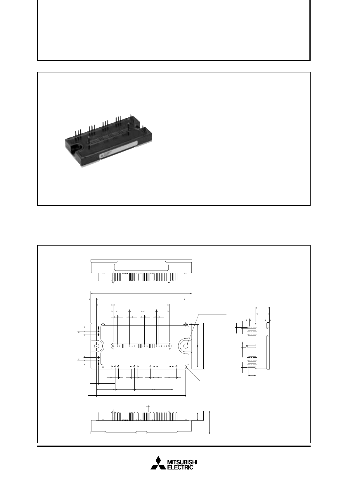
MITSUBISHI <INTELLIGENT POWER MODULES>
PM50B5LB060
FLAT-BASE TYPE
INSULATED PACKAGE
PM50B5LB060
APPLICATION
Photo voltaic power conditioner
FEATURE
TM
a) Adopting new 5th generation IGBT (CSTBT
performance is improved by 1µm fine rule process.
For example, typical V
ce(sat)=1.55V @Tj=125°C
b) Over-temperature protection by detecting Tj of the CSTBT
chips and error output is possible from all each conservation upper and lower arm of IPM.
c) New small package
Reduce the package size by 10%, thickness by 22% from
S-DASH series.
•2φ 50A, 600V Current-sense IGBT type inverter
• 50A, 600V Current-sense Chopper IGBT
• Monolithic gate drive & protection logic
• Detection, protection & status indication circuits for, shortcircuit, over-temperature & under-voltage (P-Fo available
from upper arm devices)
• UL Recognized Yellow Card No.E80276(N)
File No.E80271
) chip, which
TM
PACKAGE OUTLINES Dimensions in mm
L A B E L
120
106
7
3.25
44
NP
35
44
2.5
7.75 98.25
15
BUVW
44444444
19.5
22
±0.25
66.519.75
16 15.25
1616
6-23-23-23-2
91319
19-■0.5
17
2-φ5.5
MOUNTING HOLES
25.7525
55
4
-φ
2.5
232323
9.5
11.5
27.5
1.5
1
1.5
2-φ2.5
1
Ter minal code
1. VUPC
2. UFO
3. UP
4. VUP1
5. VVPC
6. VFO
7. VP
8. VVP1
9. NC
10. NC
16
3
9.5
11. NC
12. NC
13. VNC
14. VN1
15. NC
16. UN
17. VN
18. WN
19. Fo
Jun. 2005
INTERNAL FUNCTIONS BLOCK DIAGRAM
WNV
FONC V
NC
N1
MITSUBISHI <INTELLIGENT POWER MODULES>
PM50B5LB060
FLAT-BASE TYPE
INSULATED PACKAGE
UP V
VP V
UNVNV
VPC
NCNCNCNC
VF
VP1
V
O
UPC
UF
UP1
O
1.5k
GND IN Fo Vcc
GND SC OUTOT
GND IN Fo Vcc
GND SC OUTOT
GND IN Fo Vcc
GND SC OUTOT
N
GND IN Fo Vcc
GND SC OUTOT
W
1.5k 1.5k
VB
GND IN Fo Vcc
GND SC OUTOT
UP
MAXIMUM RATINGS (Tj = 25°C, unless otherwise noted)
INVERTER PART
Symbol Parameter Condition Ratings Unit
VCES
±IC
±ICP
PC
Tj
Collector-Emitter Voltage
Collector Current
Collector Current (Peak)
Collector Dissipation
Junction Temperature
V
D = 15V, VCIN = 15V
T
C = 25°C
T
C = 25°C
T
C = 25°C
600
50
100
131
–20 ~ +150
V
A
A
W
°C
CONVERTER PART
Symbol Parameter Condition Ratings Unit
VCES
IC
ICP
PC
IF
VR(DC)
Tj
Collector-Emitter Voltage
Collector Current
Collector Current (Peak)
Collector Dissipation
FWDi Forward Current
FWDi Rated DC Reverse Voltage
Junction Temperature
V
D = 15V, VCIN = 15V
T
C = 25°C
T
C = 25°C
T
C = 25°C (Note-1)
T
C = 25°C
T
C = 25°C
600
50
100
131
50
600
–20 ~ +150
CONTROL PART
Symbol Parameter Condition Ratings Unit
VD
VCIN
VFO
I
FO
Supply Voltage
Input Voltage
Fault Output Supply Voltage
Fault Output Current
Applied between : V
Applied between : UP-VUPC, VP-VVPC
Applied between : UFO-VUPC, VFO-VVPC, FO-VNC
Sink current at UFO, VFO, FO terminals
UP1-VUPC
VVP1-VVPC, VN1-VNC
UN • VN • WN-VNC
20
20
20
20
Jun. 2005
V
A
A
W
A
V
°C
V
V
V
mA
TOTAL SYSTEM
Symbol
V
CC(PROT)
V
CC(surge)
Tstg
Viso
Supply Voltage Protected by
SC
Supply Voltage (Surge)
Storage Temperature
Isolation Voltage
Parameter
V
D = 13.5 ~ 16.5V, Inverter Part,
j = +125°C Start
T
Applied between : P-N, Surge value
60Hz, Sinusoidal, Charged part to Base, AC 1 min.
THERMAL RESISTANCES
Symbol
Rth(j-c)Q
Rth(j-c)F
Rth(j-c)Q
Rth(j-c)F
Junction to case Thermal
Resistances
Rth(j-c)F
Rth(c-f)
Contact Thermal Resistance
(Note-1) Tc (under the chip) measurement point is below.
arm
axis
X
Y
IGBT
32.7
–10.0
Parameter
UP
FWDi
32.2
–0.2
Inverter IGBT part (per 1/4 module) (Note-1)
Inverter FWDi part (per 1/4 module) (Note-1)
Converter IGBT part (Note-1)
Converter FWDi upper part (Note-1)
Converter FWDi lower part (Note-1)
Case to fin, (per 1 module)
Thermal grease applied (Note-1)
VP WP UN VN WN
FWDi
FWDi
IGBT
82.9
63.3
62.8
–8.4
–2.0
–8.8
IGBT
38.8
8.0
Condition
Condition
FWDi
39.3
0.8
MITSUBISHI <INTELLIGENT POWER MODULES>
PM50B5LB060
FLAT-BASE TYPE
INSULATED PACKAGE
Ratings
400
500
–40 ~ +125
2500
Limits
IGBT
53.0
3.8
FWDi
52.5
–2.8
(unit : mm)
IGBT
75.6
3.8
Min.
—
—
—
—
—
—
FWDi
75.1
–2.8
Typ. Max.
—
—
—
—
—
—
0.95
1.61
0.95
0.95
1.61
0.038
Unit
V
V
°C
V
rms
Unit
°C/W
Bottom view
ELECTRICAL CHARACTERISTICS (Tj = 25°C, unless otherwise noted)
INVERTER PART
= 15V
Condition
(Fig. 5)
Symbol
CE(sat)
V
VEC
ton
trr
tc(on)
toff
tc(off)
ICES
Parameter
Collector-Emitter
Saturation Voltage
FWDi Forward Voltage
Switching Time
Collector-Emitter
Cutoff Current
D = 15V, IC = 50A
V
V
CIN = 0V (Fig. 1)
–I
C = 50A, VD = 15V, VCIN = 15V (Fig. 2)
D = 15V, VCIN = 0V↔15V
V
V
CC = 300V, IC = 50A
T
j = 125°C
Inductive Load (Fig. 3,4)
VCE = V
CES
, V
CIN
T
j = 25°C
T
j = 125°C
T
j = 25°C
T
j = 125°C
Limits
Min. Typ. Max.
—
—
—
0.3
—
—
—
—
—
—
1.7
1.55
2.2
0.7
0.1
0.2
0.9
0.2
—
—
—
—
3.3
1.4
0.2
0.4
1.8
0.4
10
Unit
V
V
µs
1
mA
Jun. 2005
 Loading...