

MITSUBISHI PM25RL1A120 Technical data
PM25RL1A120
MITSUBISHI <INTELLIGENT POWER MODULES>
PM25RL1A120
FLAT-BASE TYPE
INSULATED PACKAGE
FEATURE
Inverter + Brake + Drive & Protection IC
a) Adopting new 5th generation Full-Gate CSTBT
TM
chip
b) The over-temperature protection which detects the chip sur-
TM
face temperature of CSTBT
is adopted.
c) Error output signal is possible from all each protection up-
per and lower arm of IPM.
d) Compatible L-series package.
•3φ 25A, 1200V Current-sense and temperature sense
IGBT type inverter
• Monolithic gate drive & protection logic
• Detection, protection & status indication circuits for, shortcircuit, over-temperature & under-voltage (P-F
O available
from upper arm devices)
• UL Recognized
APPLICATION
General purpose inverter, servo drives and other motor controls
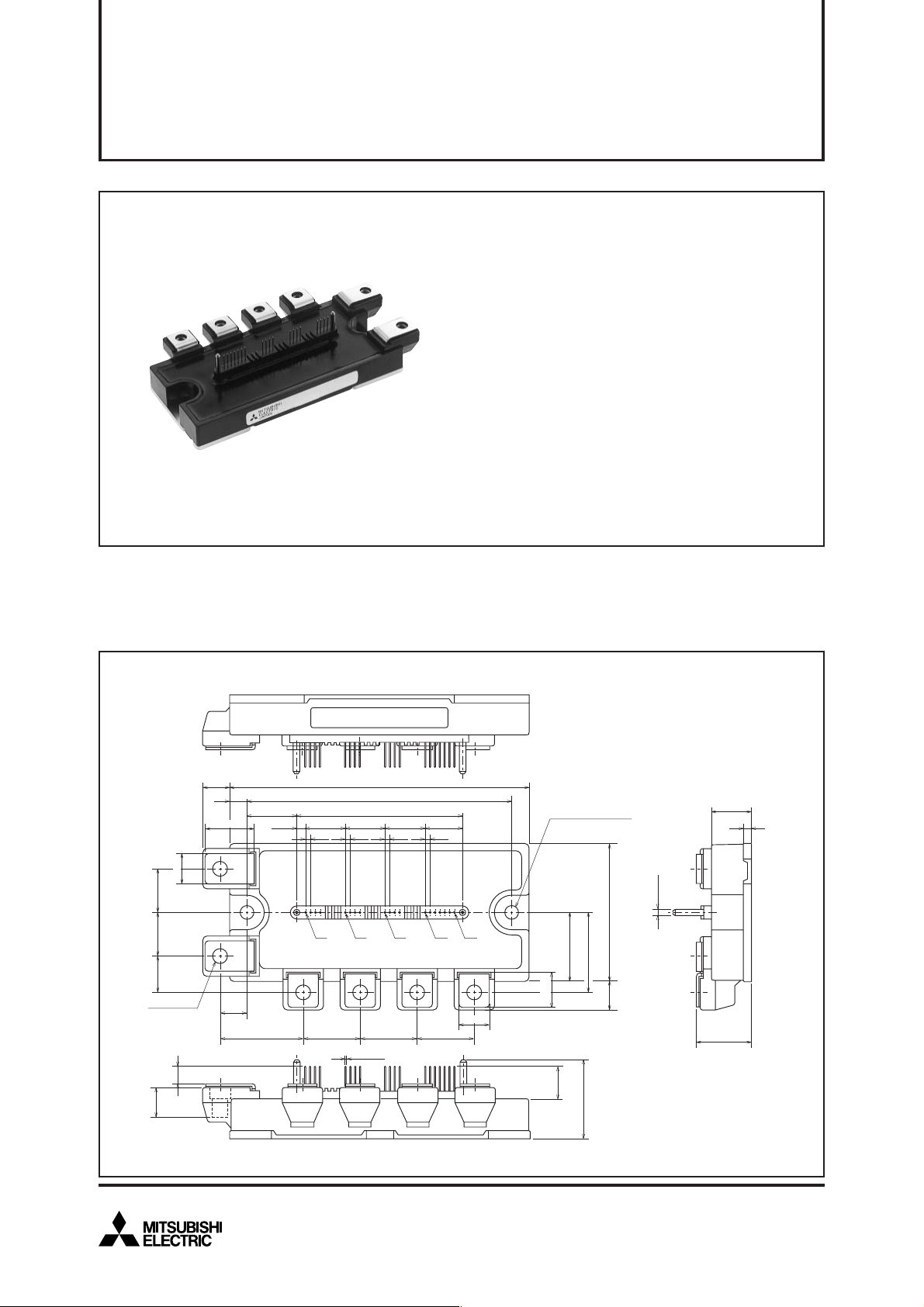
PACKAGE OUTLINES Dimensions in mm
LABEL
11
(19.75)
12
17.5 17.5
14.5
6-M5 NUTS
(7)
12
(SCREWING DEPTH)
120
7
19.75 66.5
3.25
NP
1591319
B
10.75
32.75 23 23 23
106
1616
UVW
19-■0.5
16 15.25
6-23-23-23-2
2-φ5.5
MOUNTING HOLES
2-φ2.5
55
32
27.5
(13.5)
12
13
3.15
11.75
Te rminal code
1. VUPC
2. UFO
3. UP
4. VUP1
5. VVPC
6. VFO
7. VP
16
+
22
–
8. VVP1
9. VWPC
10. WFO
11. WP
12. VWP1
13. VNC
14. VN1
1
0.5
3
15. Br
16. UN
17. VN
18. WN
19. Fo
May 2009
1
INTERNAL FUNCTIONS BLOCK DIAGRAM
V
Br
Fo
V
NC
V
N1
W
N
N
MITSUBISHI <INTELLIGENT POWER MODULES>
PM25RL1A120
FLAT-BASE TYPE
INSULATED PACKAGE
WPV
U
N
V
WPC
WF
WP1
O
V
VPC
VPV
VF
VP1
O
V
UPC
UPV
UF
UP1
O
1.5k
Gnd In Fo Vcc
Gnd Si Out OT
Gnd In Fo Vcc
Gnd Si Out OT
BNWVUP
Gnd In Fo Vcc
Gnd Si Out OT
Gnd In Fo Vcc
Gnd Si Out OT
1.5k 1.5k 1.5k
Gnd In Fo Vcc
Gnd Si Out OT
Gnd In Fo Vcc
Gnd Si Out OT
Gnd In Fo Vcc
Gnd Si Out OT
MAXIMUM RATINGS (Tj = 25°C, unless otherwise noted)
INVERTER PART
Symbol Parameter Condition Ratings Unit
VCES
±IC
±ICP
PC
Tj
Collector-Emitter Voltage
Collector Current
Collector Current (Peak)
Collector Dissipation
Junction Temperature
*: TC measurement point is just under the chip.
V
D = 15V, VCIN = 15V
T
C = 25°C (Note-1)
T
C = 25°C
T
C = 25°C (Note-1)
1200
25
50
128
–20 ~ +150
V
A
A
W
°C
BRAKE PART
Symbol Parameter Condition Ratings Unit
VCES
IC
ICP
PC
IF
VR(DC)
Tj
Collector-Emitter Voltage
Collector Current
Collector Current (Peak)
Collector Dissipation
FWDi Forward Current
FWDi Rated DC Reverse Voltage
Junction Temperature
V
D = 15V, VCIN = 15V
T
C = 25°C (Note-1)
T
C = 25°C
T
C = 25°C (Note-1)
T
C = 25°C
T
C = 25°C
1200
25
50
128
25
1200
–20 ~ +150
CONTROL PART
Symbol
VD
VCIN
V
FO
IFO
Supply Voltage
Input Voltage
Fault Output Supply Voltage
Fault Output Current
Parameter Condition Ratings Unit
Applied between : V
Applied between : UP-VUPC, VP-VVPC, WP-VWPC
Applied between : UFO-VUPC, VFO-VVPC, WFO-VWPC
Sink current at UFO, VFO, WFO, FO terminals
UP1-VUPC, VVP1-VVPC
VWP1-VWPC, VN1-VNC
UN • VN • WN • Br-VNC
FO-VNC
20
20
20
20
May 2009
2
V
A
A
W
A
V
°C
V
V
V
mA
TOTAL SYSTEM
Symbol
V
CC(PROT)
V
CC(surge)
Tstg
Viso
Parameter
Supply Voltage Protected by
SC
Supply Voltage (Surge)
Storage Temperature
Isolation Voltage
V
D = 13.5 ~ 16.5V
Inverter Part, T
Applied between : P-N, Surge value
60Hz, Sinusoidal, Charged part to Base, AC 1 min.
Condition
j = +125°C Start
THERMAL RESISTANCES
Symbol
Rth(j-c)Q
Rth(j-c)F
Rth(j-c)Q
Rth(j-c)F
Rth(c-f)
Junction to case Thermal
Resistances
Contact Thermal Resistance
Parameter
Inverter IGBT part (per 1 element) (Note-1)
Inverter FWDi part (per 1 element) (Note-1)
Brake IGBT part (Note-1)
Brake FWDi upper part (Note-1)
Case to fin, (per 1 module)
Thermal grease applied (Note-1)
* If you use this value, Rth(f-a) should be measured just under the chips.
Condition
MITSUBISHI <INTELLIGENT POWER MODULES>
PM25RL1A120
FLAT-BASE TYPE
INSULATED PACKAGE
Min.
—
—
—
—
—
Ratings
800
1000
–40 ~ +125
2500
Limits
Typ. Max.
—
—
—
—
—
0.038
0.97
1.60
0.97
1.60
Unit
V
V
°C
V
rms
Unit
°C/W
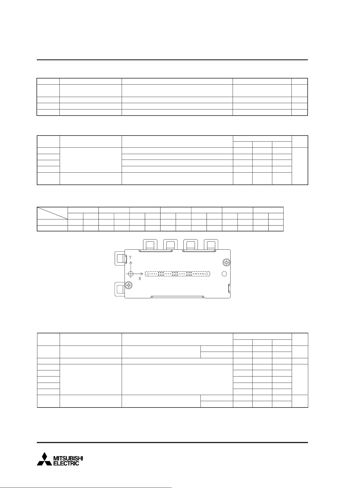
(Note-1) T
axis
C (under the chip) measurement point is below.
arm
X
Y
IGBT
27.0
–7.0
UP
FWDi
27.0
–0.2
VP WP UN VN WN BR
IGBT
FWDi
IGBT
66.9
66.9
86.5
–6.0
0.8
–6.0
FWDi
86.5
0.8
IGBT
39.2
4.0
FWDi
33.2
4.8
Bottom view
ELECTRICAL CHARACTERISTICS (Tj = 25°C, unless otherwise noted)
INVERTER PART
Symbol
CE(sat)
V
VEC
ton
trr
tc(on)
toff
tc(off)
ICES
Parameter
Collector-Emitter Saturation
Voltage
FWDi Forward Voltage
Switching Time
Collector-Emitter Cutoff
Current
D = 15V, IC = 25A
V
V
CIN = 0V, Pulsed (Fig. 1)
–I
C = 25A, VD = 15V, VCIN = 15V (Fig. 2)
D = 15V, VCIN = 0V↔15V
V
V
CC = 600V, IC = 25A
T
j = 125°C
Inductive Load (Fig. 3,4)
VCE = V
CES
, VD = 15V
Condition
(Fig. 5)
IGBT
54.3
4.0
FWDi
60.7
4.8
T
j = 25°C
T
j = 125°C
T
j = 25°C
T
j = 125°C
IGBT
FWDi
73.9
80.3
4.0
4.8
Min. Typ. Max.
—
—
—
0.3
—
—
—
—
—
—
(unit : mm)
IGBT
20.0
–7.0
Limits
1.65
1.85
2.3
0.8
0.3
0.4
1.2
0.4
—
—
Di
21.8
5.8
2.15
2.35
3.3
2.0
0.8
1.0
2.8
1.2
10
Unit
V
V
µs
1
mA
May 2009
3
 Loading...