


Sep.1998
6.0 Introduction to Intelligent
Power Modules (IPM)
Mitsubishi Intelligent Power Modules (IPMs) are advanced hybrid
power devices that combine high
speed, low loss IGBTs with optimized gate drive and protection circuitry. Highly effective over-current
and short-circuit protection is realized through the use of advanced
current sense IGBT chips that allow continuous monitoring of power
device current. System reliability is
further enhanced by the IPM’s integrated over temperature and under
voltage lock out protection. Compact, automatically assembled Intelligent Power Modules are designed to reduce system size, cost,
and time to market. Mitsubishi
Electric introduced the first full line
of Intelligent Power Modules in November, 1991. Continuous improvements in power chip, packaging, and control circuit technology
have lead to the IPM lineup shown
in Table 6.1.
6.0.1 Third Generation Intelli-
gent Power Modules
Mitsubishi third generation intelligent power module family shown in
Table 6.1 represents the industries
most complete line of IPMs. Since
their original introduction in 1993
the series has been expanded to
include 36 types with ratings ranging from 10A 600V to 800A 1200V.
The power semiconductors used in
these modules are based on the
field proven H-Series IGBT and diode processes. In Table 6.1 the
third generation family has been divided into two groups, the “Low
Profile Series” and “High Power
Series” based on the packaging
technology that is used. The third
generation IPM has been optimized
for minimum switching losses in order to meet industry demands for
acoustically noiseless inverters
with carrier frequencies up to
20kHz. The built in gate drive and
protection has been carefully designed to minimize the components
required for the user supplied interface circuit.
6.0.2 V-Series High Power IPMs
The V-Series IPM was developed
in order to address newly emerging
industry requirements for higher reliability, lower cost and reduced
EMI. By utilizing the low inductance
packaging technology developed
for the U-Series IGBT module (described in Section 4.1.5) combined
with an advanced super soft freewheel diode and optimized gate
drive and protection circuits the VSeries IPM family achieves improved performance at reduced
cost. The detailed descriptions of
IPM operation and interface requirements presented in Sections
6.1 through 6.8 apply to V-Series
as well as third generation IPMs.
The only exception being that VSeries IPMs have a unified short
circuit protection function that takes
the place of the separate short circuit and over current functions described in Sections 6.4.4 and 6.4.5.
The unified protection was made
Third Generation Low Profile Series - 600V
PM10CSJ060 10 Six IGBTs
PM15CSJ060 15 Six IGBTs
PM20CSJ060 20 Six IGBTs
PM30CSJ060 30 Six IGBTs
PM50RSK060 50 Six IGBTs + Brake ckt.
PM75RSK060 75 Six IGBTs + Brake ckt.
Third Generation Low Profile Series - 1200V
PM10CZF120 10 Six IGBTs
PM10RSH120 10 Six IGBTs + Brake ckt.
PM15CZF120 15 Six IGBTs
PM15RSH120 15 Six IGBTs + Brake ckt.
PM25RSK120 25 Six IGBTs + Brake ckt.
Third Generation High Power Series - 600V
PM75RSA060 75 Six IGBTs + Brake ckt.
PM100CSA060 100 Six IGBTs
PM100RSA060 100 Six IGBTs + Brake ckt.
PM150CSA060 150 Six IGBTs
PM150RSA060 150 Six IGBTs + Brake ckt.
PM200CSA060 200 Six IGBTs
PM200RSA060 200 Six IGBTs + Brake ckt.
PM200DSA060 200 Two IGBTs: Half Bridge
PM300DSA060 300 Two IGBTs: Half Bridge
PM400DAS060 400 Two IGBTs: Half Bridge
PM600DSA060 600 Two IGBTs: Half Bridge
PM800HSA060 800 One IGBT
Third Generation High Power Series - 1200V
PM25RSB120 25 Six IGBTs + Brake ckt.
PM50RSA120 50 Six IGBTs + Brake ckt.
PM75CSA120 75 Six IGBTs
PM75DSA120 75 Two IGBTs: Half Bridge
PM100CSA120 100 Six IGBTs
PM100DSA120 100 Two IGBTs: Half Bridge
PM150DSA120 150 Two IGBTs: Half Bridge
PM200DSA120 200 Two IGBTs: Half Bridge
PM300DSA120 300 Two IGBTs: Half Bridge
PM400HSA120 400 Two IGBTs: Half Bridge
PM600HSA120 600 One IGBT
PM800HSA120 800 One IGBT
V-Series High Power - 600V
PM75RVA060 75 Six IGBTs + Brake ckt.
PM100CVA060 100 Six IGBTs
PM150CVA060 150 Six IGBTs
PM200CVA060 200 Six IGBTs
PM300CVA060 300 Six IGBTs
PM400DVA060 400 Two IGBTs: Half Bridge
PM600DVA060 600 Two IGBTs: Half Bridge
V-Series High Power - 1200V
PM50RVA120 50 Six IGBTs + Brake ckt.
PM75CVA120 75 Six IGBTs
PM100CVA120 100 Six IGBTs
PM150CVA120 150 Six IGBTs
PM200DVA120 200 Two IGBTs: Half Bridge
PM300DVA120 300 Two IGBTs: Half Bridge
Type Number Amps Power Circuit Type Number Amps Power Circuit
Table 6.1 Mitsubishi Intelligent Power Modules
MITSUBISHI SEMICONDUCTORS POWER MODULES MOS
USING INTELLIGENT POWER MODULES
Sep.1998
possible by an advanced RTC
(Real Time Control) current clamping circuit that eliminates the need
for the over current protection function. In V-Series IPMs a unified
short circuit protection with a delay
to avoid unwanted operation replaces the over current and short
circuit modes of the third generation devices.
6.1 Structure of Intelligent
Power Modules
Mitsubishi Intelligent Power Modules utilize many of the same field
proven module packaging technologies used in Mitsubishi IGBT
modules. Cost effective implementation of the built in gate drive and
protection circuits over a wide
range of current ratings was
achieved using two different packaging techniques. Low power devices use a multilayer epoxy isolation system while medium and high
power devices use ceramic isolation. These packaging technologies
are described in more detail in Sections 6.1.1 and 6.1.2. IPM are
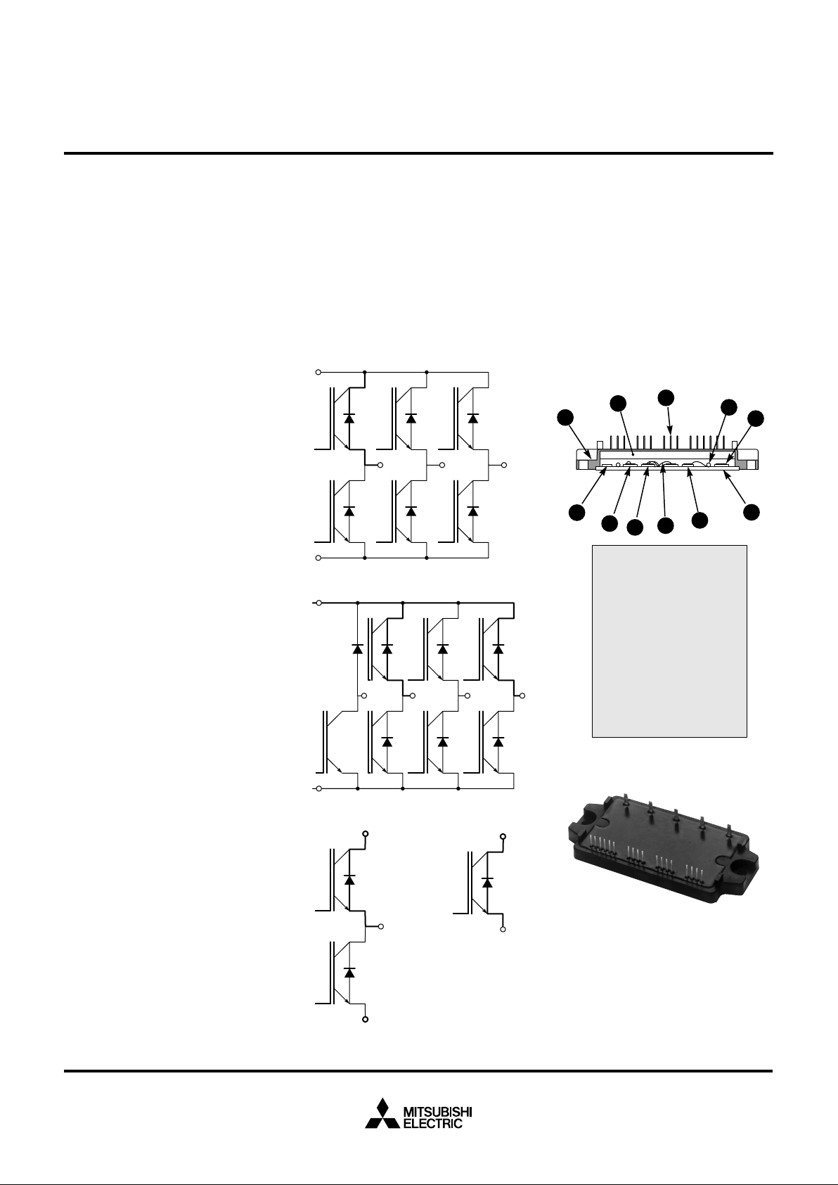
available in four power circuit configurations, single (H), dual (D), six
pack (C), and seven pack (R).
Table 6.1 indicates the power circuit of each IPM and Figure 6.1
shows the power circuit configurations.
6.1.1 Multilayer Epoxy Construc-
tion
Low power IPM (10-50A, 600V and
10-15A, 1200V) use a multilayer
epoxy based isolation system. In
this system, alternate layers of copper and epoxy are used to create a
shielded printed circuit directly on
the aluminum base plate. Power
chips and gate control circuit components are soldered directly to the
substrate eliminating the need for a
separate printed circuit board and
ceramic isolation materials. Modules constructed using this technique are easily identified by their
extremely low profile packages.
This package design is ideally
suited for consumer and industrial
applications where low cost and
compact size are important.
Figure 6.2 shows a cross section
of this type of IPM package. Figure
6.3 is a PM20CSJ060 20A, 600V
IPM.
P
UVW
C2E1
C1
E2
E
C
N
TYPE C
TYPE D
TYPE H
P
N
U
TYPE R
V WB
Figure 6.2 Multi-Layer Epoxy
Construction
Figure 6.1 Power Circuit
Configuration
Figure 6.3 PM20CSJ060
1.
2.
3.
4.
5.
6.
7.
8.
9.
10.
11.
Case
Epoxy Resin
Input Signal Terminal
SMT Resistor
Gate Control IC
SMT Capacitor
IGBT Chip
Free-wheel Diode Chip
Bond Wire
Copper Block
Baseplate with Epoxy
Based Isolation
11
10
9
8
6
7
1
2
3
4
5
MITSUBISHI SEMICONDUCTORS POWER MODULES MOS
USING INTELLIGENT POWER MODULES
Sep.1998
6.1.2 Ceramic Isolation Con-
struction
Higher power IPMs are constructed
using ceramic isolation material. A
direct bond copper process in
which copper patterns are bonded
directly to the ceramic substrate
without the use of solder is used in
these modules. This substrate provides the improved thermal characteristics and greater current carrying capabilities that are needed in
these higher power devices. Gate
drive and control circuits are contained on a separate PCB mounted
directly above the power devices.
The PCB is a multilayer construction with special shield layers for
EMI noise immunity. Figure 6.4
shows the structure of a ceramic
isolated Intelligent Power Module.
Figure 6.5 is a PM75RSA060 75 A,
600V IPM.
Figure 6.4 Ceramic Isolation Construction
Figure 6.5 PM75RSA060
SILICON CHIP
DBC PLATE
BASE
PLATE
SILICON GEL
CASE
MAIN
TERMINAL
EPOXY
RESIN
GUIDE
PIN
INPUT SIGNAL
TERMINAL
INTERCONNECT
TERMINAL
ELECTRODE
ALUMINUM WIRE
SHIELD
LAYER
RESISTOR
CONTROL BOARD
PCB
SHIELD
LAYER
SIGNAL
TRACE
MITSUBISHI SEMICONDUCTORS POWER MODULES MOS
USING INTELLIGENT POWER MODULES
Sep.1998
6.1.3 V-Series IPM Construction
V-Series IPMs are similar to the ceramic isolated types described
in Section 6.1.2 except that an insert molded case similar to the
U-Series IGBT is used. Like the
U-Series IGBT described in Section 4.1.5, the V-Series IPM
has lower internal inductance and
improved power cycle durability.
Figure 6.6 is a cross section drawing showing the construction of the
V-Series IPM. The insert molded
case makes the V-Series IPM is
easier to manufacture and lower in
cost. Figure 6.7 shows a
PM150CV A120 which is a 150A
1200V V-Series IPM.
6.1.4 Advantages of Intelligent
Power Module
IPM (Intelligent Power Module)
products were designed and developed to provide advantages to
Customers by reducing design, development, and manufacturing
costs as well as providing improvement in system performance and
reliability over conventional IGBTs.
Design and development effort is
simplified and successful drive coordination is assured by the integration of the drive and protection
circuitry directly into the IPM. Reduced time to market is only one of
the additional benefits of using an
IPM. Others include increased system reliability through automated
IPM assembly and test and reduction in the number of components
that must be purchased, stored,
and assembled. Often the system
size can be reduced through
smaller heatsink requirements as a
result of lower on-state and switching losses. All IPMs use the same
standardized gate control interface
with logic level control circuits allowing extension of the product line
without additional drive circuit design. Finally, the ability of the IPM
to self protect in fault situations reduce the chance of device destruction during development testing as
well as in field stress situations.
6.2 IPM Ratings and Characteristics
IPM datasheets are divided into
three sections:
• Maximum Ratings
• Characteristics (electrical,
thermal, mechanical)
• Recommended Operating
Conditions
The limits given as maximum rating
must not be exceeded under any
circumstances, otherwise destruction of the IPM may result.
Key parameters needed for system
design are indicated as electrical,
thermal, and mechanical characteristics.
The given recommended operating
conditions and application circuits
should be considered as a preferable design guideline fitting most
applications.
POWER TERMINALS
SILICONE GEL
COVER
INSERT MOLD CASE
DBC AIN CERAMIC
SUBSTRATE
SILICON CHIPS
BASE PLATE
PRINTED CIRCUIT
BOARD
ALUMINUM
BOND WIRES
SIGNAL TERMINALS
Figure 6.6 V-Series IPM Construction Figure 6.7 PM150CVA120
MITSUBISHI SEMICONDUCTORS POWER MODULES MOS
USING INTELLIGENT POWER MODULES

Sep.1998
6.2.1 Maximum Ratings
Symbol Parameter Definition
Inverter Part
V
CC
Supply Voltage Maximum DC bus voltage applied between P-N
V
CES
Collector-Emitter Voltage Maximum off-state collector-emitter voltage at applied control input off signal
±I
C
Collector-Current Maximum DC collector and FWDi current @ Tj ≤ 150°C
±I
CP
Collector-Current (peak) Maximum peak collector and FWDi current @ Tj ≤ 150°C
P
C
Collector Dissipation Maximum power dissipation per IGBT switch at Tj = 25°C
T
j
Junction Temperature Range of IGBT junction temperature during operation
Brake Part
V
R(DC)
FWDi Reverse Voltage Maximum reverse voltage of FWDi
I
F
FWDi Forward Current Maximum FWDi DC current at Tj ≤ 150°C
Control Part
V
D
Supply Voltage Maximum control supply voltage
V
CIN
Input Voltage Maximum voltage between input (I) and ground (C) pins
V
FO
Fault Output Supply Voltage Maximum voltage between fault output (FO) and ground (C) pins
I
FO
Fault Output Current Maximum sink current of fault output (FO) pin
Total System
V
CC(prot)
Supply Voltage Protected Maximum DC bus voltage applied between P-N with guaranteed OC and SC protection
by OC & SC
T
C
Module Case Operating Range of allowable case temperature at specified reference point during operation
Temperature
T
stg
Storage Temperature Range of allowable ambient temperature without voltage or current
V
iso
Isolation Voltage Maximum isolation voltage (AC 60Hz 1 min.) between baseplate and module terminals
(all main and signal terminals externally shorted together)
6.2.2 Thermal Resistance
Symbol Parameter Definition
R
th(j-c)
Junction to Case Maximum value of thermal resistance between junction and case per switch
Thermal Resistance
R
th(c-f)
Contact Thermal Maximum value of thermal resistance between case and fin (heatsink) per IGBT/FWDi pair
Resistance with thermal grease applied according to mounting recommendations
6.2.3 Electrical Characteristics
Symbol Parameter Definition
Inverter and Brake Part
VCE(sat) Collector-Emitter IGBT on-state voltage at rated collector current under specified conditions
Saturation Voltage
V
EC
FWDi Forward Voltage FWDi forward voltage at rated current under specified conditions
t
on
Turn-On Time
t
rr
FWDi Recovery Time Inductive load switching times under rated conditions
t
c(on)
Turn-On Crossover Time (See Figure 6.10)
t
off
Turn-Off Time
t
c(off)
Turn-Off Crossover Time
I
CES
Collector-Emitter Cutoff Collector-Emitter current in off-state at VCE = V
CES
under specified conditions
MITSUBISHI SEMICONDUCTORS POWER MODULES MOS
USING INTELLIGENT POWER MODULES

Sep.1998
The following test circuits are used
to evaluate the IPM characteristics.
1. VCE(sat) and V
EC
To ensure specified junction
temperature, Tj, measurements
of VCE(sat) and VEC must be
performed as low duty factor
pulsed tests. (See Figures 6.8
and 6.9)
6.2.3 Electrical Characteristics (continued)
Symbol Parameter Definition
Control Part
V
D
Supply Voltage Range of allowable control supply voltage in switching operation
I
D
Circuit Current Control supply current in stand-by mode
V
CIN(on)
Input ON-Voltage A voltage applied between input (I) and ground (C) pins less than this value will turn on the IPM
V
CIN(off)
Input OFF-Voltage A voltage applied between input (I) and ground (C) pins higher than this value will turn off the IPM
f
PWM
PWM Input Frequency Range of PWM frequency for VVVF inverter operations
t
dead
Arm Shoot Through Time delay required between high and low side input off/on signals to prevent an
Blocking Time arm shoot through
OC Over-Current Trip Level Collector that will activate the over-current protection
SC Short-Circuit Trip Level Collector current that will activate the short-circuit protection
t
off(OC)
Over-Current Delay Time Time delay after collector current exceeds OC trip level until OC protection is activated
OT Over-Temperature Trip Level Baseplate temperature that will activate the over-temperature protection
OT
r
Over-Temperature Temperature that the baseplate must fall below to reset an over-temperature fault
Reset Level
UV Control Supply Control supply voltage below this value will activate the undervoltage protection
Undervoltage Trip Level
UV
r
Control Supply Control supply voltage that must exceed to reset an undervoltage fault
Undervoltage Reset Level
I
FO(H)
Fault Output Inactive Current Fault output sink current when no fault has occurred
I
FO(L)
Fault Output Active Current Fault Output sink current when a fault has occurred
t
FO
Fault Output Pulsed Width Duration of the generated fault output pulse
V
SXR
SXR Terminal Output Voltage Regulated power supply voltage on SXR terminal for driving the external optocoupler
6.2.4 Recommended Operation Conditions
Symbol Parameter Definition
V
CC
Main Supply Voltage Recommended DC bus voltage range
V
D
Control Supply Voltage Recommended control supply voltage range
V
CIN(on)
Input ON-Voltage Recommended input voltage range to turn on the IPM
V
CIN(off)
Input OFF-Voltage Recommended input voltage range to turn off the IPM
f
PWM
PWM Input Frequency Recommended range of PWM carrier frequency using the recommended application circuit
t
DEAD
Arm Shoot Through Recommended time delay between high and low side off/on signals to the optocouplers
Blocking Time using the recommended application circuit
VX1
SXR
CX1
VXC
E1(E2)
C1(C2)
V
D
V
I
C
VX1
SXR
CX1
VXC
E1(E2)
C1(C2)
V
D
V
I
C
Figure 6.8 VCE(sat) Test
Figure 6.9 VEC Test
6.2.5 Test Circuits and Conditions
MITSUBISHI SEMICONDUCTORS POWER MODULES MOS
USING INTELLIGENT POWER MODULES
Sep.1998
2. Half-Bridge Test Circuit and
Switching Time Definitions.
Figure 6.10 shows the stan-
dard half-bridge test circuit and
switching waveforms. Switching times and FWDi recovery
characteristics are defined as
shown in this figure.
3. Overcurrent and
Short-Circuit Test
I
trip
levels and timing specifications in short circuit and
overcurrent are defined as
shown in Figure 6.11. By using
a fixed load resistance the supply voltage, VCC, is gradually
increased until OC and SC trip
levels are reached.
Precautions:
A. Before applying any main bus
voltage, VCC, the input terminals should be pulled up by resistors to their corresponding
control supply (or SXR) pin,
each input signal should be
kept in OFF state, and the control supply should be provided.
After this, the specified ON and
OFF level for each input signal
should be applied. The control
supply should also be applied
to the non-operating arm of the
module under test and inputs
of these arms should be kept
to their OFF state.
B. When performing OC and SC
tests the applied voltage, VCC,
must be less than V
CC(prot)
and the turn-off surge voltage
spike must not be allowed to
rise above the V
CES
rating of
the device. (These tests must
not be attempted using a
curve tracer.)
+
I
C
INTEGRATED
GATE
CONTROL
CIRCUIT
INTEGRATED
GATE
CONTROL
CIRCUIT
+
+
t
d (on)
I
CIN
(t
on
=
t
d (on
)
+ tr)
t
r
t
d (off)
(t
off
= t
d (off)
+
tf)
t
f
t
c (off)
t
c (on)
10%
90%
10%
90%
I
C
t
rr
I
rr
V
CE
I
C
V
CE
OFF
SIGNAL
ON
PULSE
V
CC
V
D
V
D
Figure 6.10 Half-Bridge Test Circuit and Switching Time Definitions
ON
PULSE
SC
OC
INPUT
SIGNAL
NORMAL
OPERATION
OVER
CURRENT
SHORT
CIRCUIT
V
C
ON
PULSE
R*
R IS SIZED TO CAUSE
SC AND OC CONDITIONS
*
V
CC
+
t
off
(OC)
I
C
INTEGRATED
GATE
CONTROL
CIRCUIT
SC
OC
SC
OC
I
C
I
C
I
C
Figure 6.11 Over-Current and Short-Circuit Test Circuit
MITSUBISHI SEMICONDUCTORS POWER MODULES MOS
USING INTELLIGENT POWER MODULES

Sep.1998
6.3 Area of Safe Operation for
Intelligent Power Modules
The IPMs built-in gate drive and
protection circuits protect it from
many of the operating modes that
would violate the Safe Operation
Area (SOA) of non-intelligent IGBT
modules. A conventional SOA definition that characterizes all possible combinations of voltage, current, and time that would cause
power device failure is not required. In order to define the SOA
for IPMs, the power device capability and control circuit operation
must both be considered. The resulting easy to use short circuit and
switching SOA definitions for Intelligent Power Modules are summarized
in this section.
6.3.1 Switching SOA
Switching or turn-off SOA is normally defined in terms of the maximum allowable simultaneous voltage and current during repetitive
turn-off switching operations. In the
case of the IPM the built-in gate
drive eliminates many of the dangerous combinations of voltage
and current that are caused by improper gate drive. In addition, the
maximum operating current is limited by the over current protection
circuit. Given these constraints the
switching SOA can be defined using the waveform shown in Figure
6.12. This waveform shows that the
IPM will operate safely as long as
the DC bus voltage is below the
data sheet V
CC(prot)
specification,
the turn-off transient voltage across
C-E terminals of each IPM switch is
maintained below the V
CES
specification, Tj is less than 125°C, and
the control power supply voltage is
between 13.5V and 16.5V. In this
waveform IOC is the maximum current that the IPM will allow without
causing an Over Current (OC) fault
to occur. In other words, it is just
below the OC trip level. This waveform defines the worst case for
hard turn-off operations because
the IPM will initiate a controlled
slow shutdown for currents higher
than the OC
trip level.
6.3.2 Short Circuit SOA
The waveform in Figure 6.13 depicts typical short circuit operation.
The standard test condition uses a
minimum impedance short circuit
which causes the maximum short
circuit current to flow in the device.
In this test, the short circuit current
(ISC) is limited only by the device
characteristics. The IPM is guaranteed to survive non-repetitive short
circuit and over current conditions
as long as the initial DC bus voltage is less than the V
CC(prot)
specification, all transient voltages
across C-E terminals of each IPM
switch are maintained less than the
V
CES
specification, Tj is less than
125°C, and the control supply voltage is between 13.5V and 16.5V.
The waveform shown depicts the
controlled slow shutdown that is
used by the IPM in order to help
minimize transient voltages.
Note:
The condition VCE ≤ V
CES
has to
be carefully checked for each IPM
switch. For easing the design another rating is given on the data
sheets, V
CC(surge)
, i.e., the maximum allowable switching surge
voltage applied between the P and
N terminals.
6.3.3 Active Region SOA
Like most IGBTs, the IGBTs used in
the IPM are not suitable for linear
or active region operation. Normally device capabilities in this
mode of operation are described in
terms of FBSOA (Forward Biased
Safe Operating Area). The IPM’s
internal gate drive forces the IGBT
to operate with a gate voltage of either zero for the off state or the
control supply voltage (VD) for the
on state. The IPMs under-voltage
lock out prevents any possibility of
active or linear operation by automatically turning the power device
off if VD drops to a level
that could cause desaturation of
the IGBT.
Figure 6.13 Short-Circuit
Operation
Figure 6.12 Turn-Off Waveform
I
OC
≤V
CES
≤V
CC(PROT)
t
off(OC)
≤V
CES
≤V
CES
≤V
CC(PROT)
I
SC
MITSUBISHI SEMICONDUCTORS POWER MODULES MOS
USING INTELLIGENT POWER MODULES

Sep.1998
6.4. IPM Self Protection
6.4.1 Self Protection Features
IPM (Intelligent Power Modules)
have sophisticated built-in protection circuits that prevent the power
devices from being damaged
should the system malfunction or
be over stressed. Our design and
applications engineers have developed fault detection and shut down
schemes that allow maximum utilization of power device capability
without compromising reliability.
Control supply under-voltage, overtemperature, over-current, and
short-circuit protection are all provided by the IPM's internal gate
control circuits. A fault output signal
is provided to alert the system controller if any of the protection circuits are activated. Figure 6.14 is a
block diagram showing the IPMs
internally integrated functions. This
diagram also shows the isolated interface circuits and control power
supply that must be provided by
the user. The internal gate control
circuit requires only a simple +15V
DC supply. Specially designed gate
drive circuits eliminate the need for
a negative supply to off bias the
IGBT. The IPM control input is designed to interface with
optocoupled transistors with a minimum of external components. The
operation and timing of each protection feature is described in Sections 6.4.2 through 6.4.5.
6.4.2 Control Supply
Under-Voltage Lock-Out
The Intelligent Power Module's internal control circuits operate from
an isolated 15V DC supply. If, for
any reason, the voltage of this supply drops below the specified under-voltage trip level (UVt), the
power devices will be turned off
and a fault signal will be generated.
Small glitches less than the specified t
dUV
in length will not affect the
operation of the control circuitry
and will be ignored by the undervoltage protection circuit. In order
for normal operation to resume, the
supply voltage must exceed the under-voltage reset level (UVr). Operation of the under-voltage protection circuit will also occur during
power up and power down of the
control supply. This operation is
normal and the system controller's
program should take the fault output delay (tfo) into account. Figure
6.15 is a timing diagram showing
the operation of the under-voltage
lock-out protection circuit. In this
diagram an active low input signal
is applied to the input pin of the
IPM by the system controller. The
effects of control supply power up,
power down and failure on the
power device gate drive and fault
output are shown.
Caution:
1. Application of the main bus
voltage at a rate greater than
20V/µs before the control
power supply is on and stabilized may cause destruction of
the power devices.
2. Voltage ripple on the control
power supply with dv/dt in excess of 5V/µs may cause a
false trip of the UV lock-out.
6.4.3 Over-Temperature
Protection
The Intelligent Power Module has a
temperature sensor mounted on
the isolating base plate near the
IGBT chips. If the temperature of
the base plate exceeds the overtemperature trip level (OT) the
IPMs internal control circuit will
protect the power devices by disabling the gate drive and ignoring
the control input signal until the
over temperature condition has
subsided. In six and seven pack
modules all three low side devices
will be turned off and a low side
fault signal will be generated. High
side switches are unaffected and
can still be turned on and off by the
system controller. Similarly, in dual
type modules only the low side device is disabled. The fault output
will remain as long as the overtemperature condition exists. When
the temperature falls below the
over-temperature reset level (OTr),
and the control input is high (offstate) the power device will be enabled and normal operation will resume at the next low (on) input signal. Figure 6.16 is a timing diagram
showing the operation of the over-
GATE
CONTROL
CIRCUIT
GATE DRIVE
OVER TEMP
UV LOCK-OUT
OVER CURRENT
SHORT CIRCUIT
ISOLATED
POWER
SUPPLY
ISOLATING
INTERFACE
CIRCUIT
ISOLATING
INTERFACE
CIRCUIT
CURRENT
SENSE
IGBT
TEMPERATURE
SENSOR
SENSE
CURRENT
INTELLIGENT POWER MODULE
INPUT
SIGNAL
FAULT
OUTPUT
COLLECTOR
EMITTER
Figure 6.14 IPM Functional Diagram
MITSUBISHI SEMICONDUCTORS POWER MODULES MOS
USING INTELLIGENT POWER MODULES

Sep.1998
temperature protection circuit.
The over temperature function provides effective protection against
overloads and cooling system failures in most applications. However,
it does not guarantee that the maximum junction temperature rating of
the IGBT chip will never be exceeded. In cases of abnormally
high losses such as failure of the
system controller to properly regulate current or excessively high
switching frequency it is possible
for IGBT chip to exceed T
j(max)
before the base plate reaches the OT
trip level.
Caution:
Tripping of the over-temperature
protection is an indication of stressful operation. Repetitive tripping
should be avoided.
6.4.4 Over-Current Protection
The IPM uses current sense IGBT
chips to continuously monitor
power device current. If the current
though the Intelligent Power Module exceeds the specified
overcurrent trip level (OC) for a period longer than t
off(OC)
the IPMs
internal control circuit will protect
the power device by disabling the
gate drive and generating a fault
output signal. The timing of the
over-current protection is shown in
Figure 6.17. The t
off(OC)
delay is
implemented in order to avoid tripping of the OC protection on short
pulses of current above the OC
level that are not dangerous for the
power device. When an over-cur-
rent is detected a controlled shutdown is initiated and a fault output
is generated. The controlled shutdown lowers the turn-off di/dt which
helps to control transient voltages
that can occur during
shut down from high fault currents.
Most Intelligent Modules use the
two step shutdown depicted in Figure 6.17. In the two step shutdown,
the gate voltage is reduced to an
intermediate voltage causing the
current through the device to drop
slowly to a low level. Then, about
5µs later, the gate voltage is reduced to zero completing the shut
down. Some of the large six and
seven pack IPMs use an active
ramp of gate voltage to achieve the
desired reduction in turn off di/dt
under high fault currents. The oscillographs in Figure 6.18 illustrate
Figure 6.15 Operation of Under-Voltage Lockout
INPUT
SIGNAL
BASE PLATE
TEMPERATURE
(Tb)
FAULT OUTPUT
CURRENT
(I
FO
)
INTERNAL
GATE
VOLTAGE
V
GE
OT
OT
r
Figure 6.16 Operation of Over-Temperature
INPUT
SIGNAL
CONTROL
SUPPLY
VOLTAGE
FAULT
OUTPUT
CURRENT
(I
FO
)
INTERNAL
GATE
VOLTAGE
V
GE
CONTROL SUPPLY ON SHORT
GLITCH
IGNORED
POWER SUPPLY
FAULT AND
RECOVERY
CONTROL SUPPLY OFF
UV
r
UV
t
t
FO
t
dUV
t
FO
t
dUV
MITSUBISHI SEMICONDUCTORS POWER MODULES MOS
USING INTELLIGENT POWER MODULES
 Loading...