

Mitsubishi MH4M365CNXJ-5, MH4M365CNXJ-6, MH4M365CXJ-6, MH4M365CXJ-7, MH4M365CXJ-5 Datasheet
...
MITSUBISHI LSIs
MH4M365CXJ/CNXJ-5,-6,-7
HYPER PAGE MODE 150994944-BIT ( 4194304-WORD BY 36-BIT ) DYNAMIC RAM
PIN CONFIGURATION (TOP VIEW)
DESCRIPTION
The MH4M365CXJ/CNXJ is 4194304-word x 36-bits dynamic
RAM. This consists of eight industry standard 4M x 4 dynamic
RAMs in SOJ and four industry 4M x 1 dyanmic RAMs in SOJ.
The mounting of SOJ on a single in-line package provides any
application where high densities and large quantities of memory
are required. This is a socket-type memory module,suitable for
easy interchange or addition of modules.
FEATURES
Type name
MH4M365CXJ/CNXJ-5
MH4M365CXJ/CNXJ-6
MH4M365CXJ/CNXJ-7
access
time
(max.ns)
Address
time
(max.ns)
access
time
(max.ns)
506013152530 90
70 20 35 130
access
Cycle
time
(min.ns)
110
Power
dissipa-
tion
(typ.mW)
7240
5920
5200
RAS
CAS
72pin single in-line package
Single 5.0V ± 10% supply
Low stand-by power dissipation
44mW (Max) CMOS lnput level
Low operating power dissipation
MH4M365CXJ/CNXJ- 5 9.15W (Max)
MH4M365CXJ/CNXJ- 6 7.48W (Max)
MH4M365CXJ/CNXJ- 7 6.51W (Max)
Hyper-page mode , RAS-only refresh , CAS before RAS
refresh, Hidden refresh capabilities
All inputs and output directly TTL compatible
2048 refresh cycles every 32ms (A0 ~ A10)
MH4M365CXJ Gold plating
MH4M365CNXJ Nickel+solder plating
APPLICATION
Main memory unit for computers, Microcomputer memory,
Refresh memory for CRT
1.Vss
2.DQ0
3.DQ16
4.DQ1
5.DQ17
6.DQ2
7.DQ18
8.DQ3
11.NC
10.Vcc
11.NC
12.A0
13.A1
14.A2
15.A3
16.A4
17.A5
18.A6
19.A10
20.DQ4
21.DQ20
22.DQ5
23.DQ21
24.DQ6
25.DQ22
26.DQ7
27.DQ23
28.A7
29.NC
30.Vcc
31.A8
32.A9
33.NC
34.RAS2
35.MP2
36.MP0
37.MP1
38.MP3
39.Vss
40.CAS0
41.CAS2
42.CAS3
43.CAS1
44.RAS0
45.NC
46.NC
47.W
48.NC
49.DQ8
50.DQ24
51.DQ9
52.DQ25
53.DQ10
54.DQ26
55.DQ11
56.DQ27
57.DQ12
58.DQ28
59.Vcc
60.DQ29
61.DQ13
62.DQ30
63.DQ14
64.DQ31
65.DQ15
66.NC
67.PD1
68.PD2
69.PD3
70.PD4
71.NC
72.Vss
[Double side]
1
2
3
4
5
6
7
8
9
10
11
12
13
14
15
16
17
18
19
20
21
22
23
24
25
26
27
28
29
30
31
32
33
34
35
36
37
38
39
40
41
42
43
44
45
46
47
48
49
50
51
52
53
54
55
56
57
58
59
60
61
62
63
64
65
66
67
68
69
70
71
72
MIT-DS-0086-1.1
PD1
PD2
PD3
PD4
MITSUBISHI
ELECTRIC
( / 15 )
1
- 5 - 6
Vss Vss
NCNC
Vss
NC
Vss
NC
- 7
Vss
NC
Vss
NC
Outline 72N9D-C
NC: NO CONNECTION
Nov.8.96

MH4M365CXJ/CNXJ-5,-6,-7
HYPER PAGE MODE 150994944-BIT ( 4194304-WORD BY 36-BIT ) DYNAMIC RAM
FUNCTION
in addition to normal read, write, a number of other
functions, e.g., hyper page mode, RAS only refresh,
Table 1 Input conditions for each mode
Operation
Read ACT ACT NAC
Early write
RAS-only refresh
Hidden refresh
CAS before RAS refresh
Standby
Note : ACT : active, NAC : nonactive, DNC : don' t care, VLD : valid, IVD : Invalid,APD : applied, OPN : open
RAS
ACT ACT ACT
ACT
ACT
ACT ACT DNC
NAC
CAS
NAC
ACT
DNC
W
DNC
NAC
DNC
BLOCK DIAGRAM
The input conditions for each are shown in Table 1.
Inputs
Row
address
Column
APD APD
APD APD
APD
APD
DNC DNC
DNC
address
DNC
DNC
DNC
Input/Output
Input
VLD OPN
DNC
DNC
DNC OPN
Output
VLDOPN
OPN
VLDOPN
OPN
MITSUBISHI LSIs
DQ0
DQ1
DQ2
DQ3
DQ4
DQ5
DQ6
DQ7
DQ8
DQ9
DQ10
DQ11
DQ12
DQ13
DQ14
DQ15
MP0 MP1 MP2 MP3
DQ16
DQ17
DQ18
DQ19
2 4 6 8 20 22 24 26 49 5153 55 57 6163 65 3 5 7 9 2123 25 27 50 52 54 56 58 60 62 6436 37 35 38
M5M
417405CJ
40 44 43 34 474241
CAS0
RAS0
M5M
417405CJ
M5M
417405CJ
M5M
417405CJ
M5M
44105CJ
M5M
44105CJ
M5M
44105CJ
M5M
44105CJ
M5M
417405CJ
12 13 14 15 16 17 18 28 31 32 19
CAS1 CAS2 CAS3 W
A0A1A2A3A4A5A6A7A8A9A10
DQ20
DQ21
DQ22
M5M
417405CJ
DQ23
DQ24
DQ25
DQ26
M5M
417405CJ
DQ27
DQ28
DQ29
DQ30
M5M
417405CJ
RAS2
DQ31
MIT-DS-0086-1.1
MITSUBISHI
ELECTRIC
( / 15 )
2
Nov.8.96

HYPER PAGE MODE 150994944-BIT ( 4194304-WORD BY 36-BIT ) DYNAMIC RAM
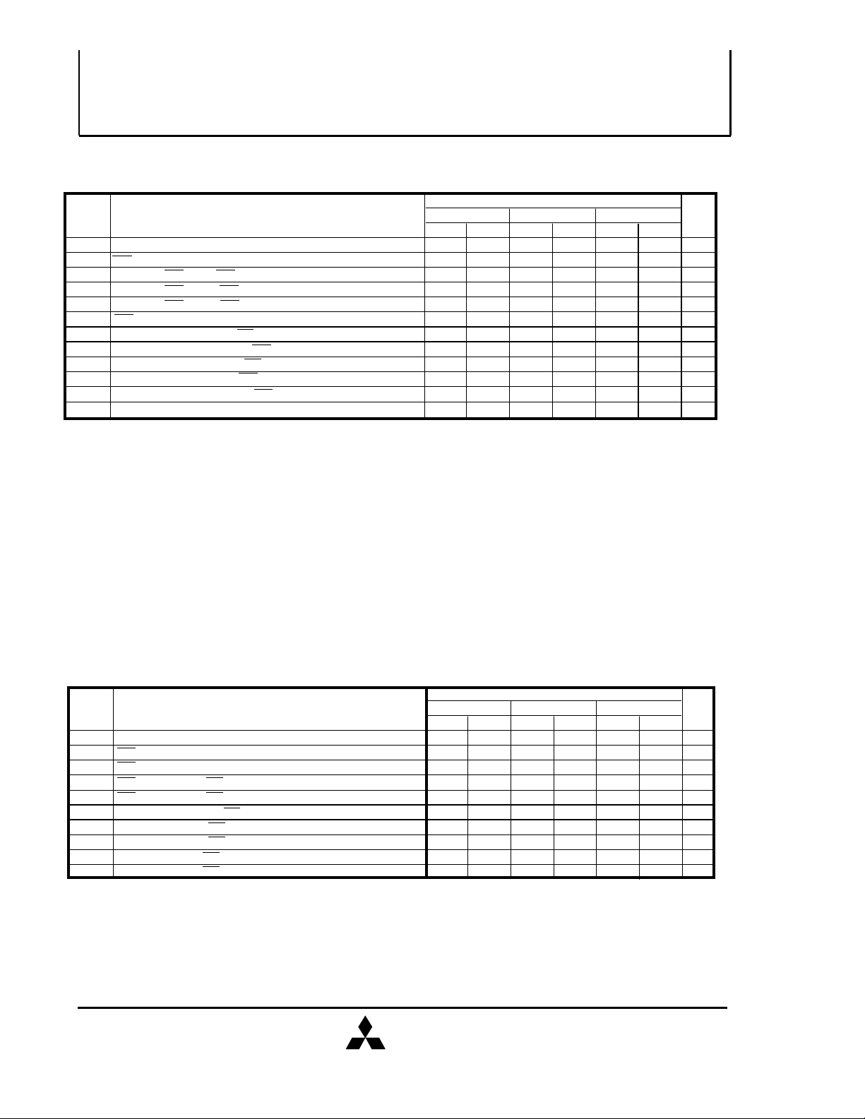
ABSOLUTE MAXIMUM RATINGS
Symbol
Vcc
V I
V0
I 0
Pd
Topr
Tstg
Supply voltage
Input voltage
Output voltage
Output current
Power dissipation
Operating temperature
Storage temperature
Parameter Conditions Ratings Unit
MITSUBISHI LSIs
MH4M365CXJ/CNXJ-5,-6,-7
With respect to Vss
Ta=25 C
-1 ~ 7
-1 ~ 7
-1 ~ 7
50
12
0 ~ 70
-40 ~ 125
V
V
V
mA
W
C
C
RECOMMENDED OPERATING CONDITIONS
Symbol
Vcc
Vss
VIH
VIL
Note 1 : All voltage values are with respect to Vss
Supply voltage
Supply voltage
High-level input voltage, all inputs
Low-level input voltage, all inputs
ELECTRICAL CHARACTERISTICS
Symbol
VOH
VOL
IOZ
I I
ICC1 (AV)
ICC2
ICC3 (AV)
ICC4(AV)
ICC6(AV)
Note 2: Current flowing into an IC is positive, out is negative.
3: Icc1 (AV), Icc3 (AV) and Icc4 (AV) are dependent on cycle rate. Maximum current is measured at the fastest cycle rate.
4: Icc1 (AV) and Icc4 (AV) are dependent on output loading. Specified values are obtained with the output open.
5: Column Address can be changed once or less while RAS=VIL and CAS=VIH .
High-level output voltage
Low-level output voltage
Off-state output current
Input current
Average supply current
from Vcc operating
Supply current from Vcc , stand-by
Average supply current
from Vcc refreshing
Average supply current
from Vcc
Hyper-Page-Mode
Average supply current
from Vcc
CAS before RAS refresh
mode
Parameter
Parameter
(Note 3,4,5)
(Note 3,5)
(Note 3,4,5)
(Note 3)
(Ta=0 ~ 70°C, Vcc=5.0V ± 10%, Vss=0V, unless otherwise noted) (Note 2)
MH4M365C -5
MH4M365C -6
MH4M365C -7
(Note 6)
MH4M365C -5
MH4M365C -6
MH4M365C -7
MH4M365C -5
MH4M365C -6
MH4M365C -7
MH4M365C -5
MH4M365C -6
MH4M365C -7
(Ta=0 ~ 70 °C, unless otherwise noted) (Note 1)
Limits
Min Nom Max
5.5
5.0
4.5
0
0
0
2.4
-1
IOH=-5.0mA
IOL=4.2mA
Q floating 0V ≤ VOUT ≤ 5.5V
0V ≤ VIN ≤ 6 V, Other inputs pins=0V
RAS, CAS cycling
tRC=tWC=min.
output open
RAS= CAS =VIH, output open
RAS= CAS ≥ Vcc - 0.2 V
RAS cycling, CAS= VIH
tRC=min.
output open
RAS=VIL, CAS cycling
tPC=min.
output open
CAS before RAS refresh cycling
tRC=min.
output open
5.5
0.8
Test conditions
Unit
V
V
V
V
Limits
Min Max
Typ
2.4
0
-20
-120
1660
1360
1180
1660
1360
1180
1620
1320
1060
1580
1300
1140
Vcc
120
0.4
20
Unit
V
V
µA
µA
mA
24
mA
8
mA
mA
mA
MIT-DS-0086-1.1
MITSUBISHI
ELECTRIC
( / 15 )
3
Nov.8.96

MITSUBISHI LSIs
MH4M365CXJ/CNXJ-5,-6,-7
HYPER PAGE MODE 150994944-BIT ( 4194304-WORD BY 36-BIT ) DYNAMIC RAM
CAPACITANCE
Symbol Parameter
CI (W)
CI (RAS)
CI (CAS)
CI / O
(Ta=0 ~ 70 °C, Vcc=5.0V ± 10%, Vss=0V, unless otherwise noted)
Input capacitance,address inputsCI (A)
Input capacitance, write control input
Input capacitance, RAS input
Input capacitance, CAS input
Input/Output capacitance, data ports
SWITCHING CHARACTERISTICS
Symbol
tCAC
tRAC
tAA
tCPA
tOHC
tOHR
tCLZ
tWEZ
tOFF
tREZ
Access time from CAS
Access time from RAS
Column address access time
Access time from CAS precharge
Output hold time from CAS 5
Output hold time from RAS
Output low impedance time from CAS low (Note 7) 5
Output disable time after WE high
Output disable time after CAS high
Output disable time after RAS high
Parameter
Test conditions
VI=Vss
f=1MHZ
Vi=25mVrms
(Ta=0 ~ 70 °C, Vcc = 5V ± 10%, Vss=0V, unless otherwise noted , see notes 6,14,15)
MH4M365C -5
Min Max
(Note 7,8)
(Note 7,9)
(Note 7,10)
(Note 7,11)
(Note 13)
(Note 12)
(Note 12,13)
(Note 12,13)
13
50
25
30
5
5
13
13
13
Limits
Min Max
Typ
78
84
42
42
22
Limits
MH4M365C -6 MH4M365C -7
Min Max
5
55 ns
Min Max
15
60
30
35
5
15
15
15
Unit
pF
pF
pF
pF
pF
Unit
ns
20
ns
70
ns
35
ns
40
ns5
ns
ns
20
ns
20
ns
20
Note 6: An initial pause of 500µs is required after power-up followed by a minimum of eight initialization cycles (any combination of cycles
containing a RAS clock such as RAS-Only refresh).
Note the RAS may be cycled during the initial pause . And any 8 RAS or RAS/CAS cycles are required after prolonged periods
(greater than 32 ms) of RAS inactivity before proper device operation is achieved.
7: Measured with a load circuit equivalent to VOH=2.4V(IOH=-5mA) / VOL=0.4V(IOL=-4.2mA) load 100pF.
The reference levels for measuring of output signal are 2.0V(VOH) and 0.8V(VOL).
8: Assumes that tRCD ≥ tRCD(max) and tASC ≥ tASC(max) and tCP ≥t CP(max).
9: Assumes that tRCD ≤ tRCD(max) and tRAD ≤ tRAD(max). If tRCD or tRAD is greater than the maximum recommended value shown in this table,
tRAC will increase by amount that tRCD exceeds the value shown.
10: Assumes that tRAD ≥ tRAD(max) and tASC ≤ tASC(max).
11: Assumes that tCP ≤ tCP(max) and tASC ≥ tASC(max).
12: tWEZ(max) ,tOFF(max) and tREZ(max)defines the time at which the output achieves the high impedance state ( IOUT ≤ I ± 10 µA I)
and is not reference to VOH(min) or VOL(max).
13: Output is disabled after both RAS and CAS go to high.
MIT-DS-0086-1.1
MITSUBISHI
Nov.8.96
ELECTRIC
( / 15 )
4
MH4M365CXJ/CNXJ-5,-6,-7
HYPER PAGE MODE 150994944-BIT ( 4194304-WORD BY 36-BIT ) DYNAMIC RAM
TIMING REQUIREMENTS (For Read, Write, Refresh, and Hyper-Page Mode Cycles)
(Ta=0 ~ 70°C, Vcc = 5V ± 10%, Vss=0V, unless otherwise noted See notes 14,15)
MITSUBISHI LSIs
40
20
5
0
10
15
0
0
10
10
1
Limits
32
45
30
13
50
Min Max
32
50
50
20
5
0
13
35
15
0
0
10
10
50
1
Unit
13
Symbol
tREF
tRP
tRCD
tCRP
tRPC
tCPN
tRAD
tASR
tASC
tRAH
tCAH
tT
Note 14: The timing requirements are assumed tT =3ns.
15: VIH(min) and VIL(max) are reference levels for measuring timing of input signals.
16: tRCD(max) is specified as a reference point only. If tRCD is less than tRCD(max), access time is tRAC. If tRCD is greater than tRCD(max), access
time is controlled exclusively by tCAC or tAA.
17: tRAD(max) is specified as a reference point only. If tRAD ≤ tRAD(max) and tASC ≤ tASC(max), access time is controlled exclusively by tAA.
18: tASC(max) is specified as a reference point only. If tRCD ≥ tRCD(max) and tASC ≥ tASC(max), access time is controlled exclusively by tCAC.
19: tT is measured between VIH(min) and VIL(max).
Refresh cycle time
RAS high pulse width
Delay time, RAS low to CAS low
Delay time, CAS high to RAS low
Delay time, RAS high to CAS low
CAS high pulse width
Column address delay time from RAS low
Row address setup time before RAS low
Column address setup time before CAS low
Row address hold time after RAS low
Column address hold time after CAS low
Transition time
Parameter
(Note16)
(Note17)
(Note18)
(Note19)
MH4M365C -5 MH4M365C -6 MH4M365C -7
Min Max Min Max
32
30
18
5
8
13
8
8
37
0
25
0
10
0
50
1
ms
ns
ns
ns
ns
ns
ns
ns
ns
ns
ns
ns
Read and Refresh Cycles
Symbol
Read cycle time
tRC
RAS low pulse width
tRAS
CAS low pulse width
tCAS
CAS hold time after RAS low
tCSH
RAS hold time after CAS low
tRSH
Read Setup time before CAS low
tRCS
Read hold time after CAS high (Note 20)
tRCH
Read hold time after RAS high
tRRH
Column address to RAS hold time
tRAL
Column address to CAS hold time
tCAL
Note 20: Either tRCH or tRRH must be satisfied for a read cycle.
Parameter
(Note 20)
MIT-DS-0086-1.1
MH4M365C -5 MH4M365C -6 MH4M365C -7
Min Max Min Max
90
50
8
40
13
0
0
0
25
13 18
MITSUBISHI
ELECTRIC
( / 15 )
5
10000
10000
110
60
10
48
30
Limits
15
0
0
0
10000
10000
Min Max
130
10000
70
10000
13
55
20
0
0
0
35
23
Unit
ns
ns
ns
ns
ns
ns
ns
ns
ns
ns
Nov.8.96
 Loading...