Mitsubishi MH32D64AKQJ-10 Datasheet
2,147,483,684
-BIT (33,554,432-WORD BY 64-BIT) Double Data Rate Synchronous DRAM Module
Preliminary Spec.
APPLICATION
Type name
133MHz
MH32D64AKQJ-10
MH32D64AKQJ-75
Frequency
100MHz
Data Rate(DDR) Synchronous DRAM mounted module.
main
[component level]
+ 0.75ns
+ 0.8ns
- Module 2bank Configration
Some contents are subject to change without notice.
MITSUBISHI LSIs
MH32D64AKQJ-75,-10
DESCRIPTION
The MH32D64AKQJ is 33554432 - word x 64-bit Double
This consists of 8 industry standard 16M x 16 DDR
Synchronous DRAMs in TSOP with SSTL_2 interface which
achieves very high speed data rate up to 133MHz.
This socket-type memory module is suitable for
memory in computer systems and easy to interchange or
add modules.
FEATURES
Max.
CLK
Access Time
- Utilizes industry standard 16M X 16 DDR Synchronous DRAMs
in TSOP package , industry standard EEPROM(SPD) in
TSSOP package
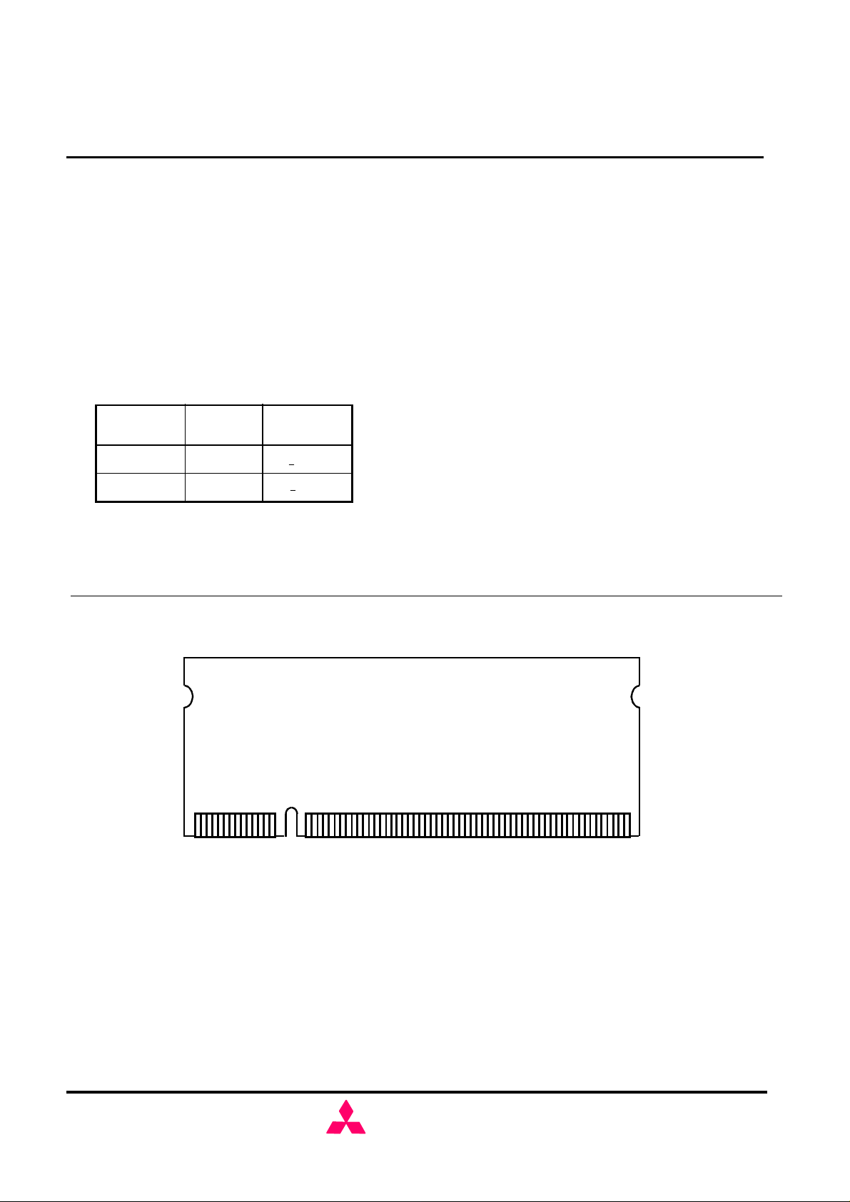
- 200pin SO-DIMM
- Vdd=Vddq=2.5v±0.2V
- Double data rate architecture; two data transfers per
clock cycle
- Bidirectional, data strobe (DQS) is transmitted/received
with data
- Differential clock inputs (CLK and /CLK)
- DLL aligns DQ and DQS transitions with CLK transition edges of DQS
- Commands entered on each positive CLK edge
- Data and data mask referenced to both edges of DQS
- 4bank operation concontrolled byBA0,BA1(Bank Address
,discrete)
- /CAS latency- 2.0/2.5 (programmable)
- Burst length- 2/4/8 (programmable)
- Burst Type - sequential/interleave(programmable)
- Auto precharge / All bank precharge controlled by A10
- 8192 refresh cycles /64ms
- Auto refresh and Self refresh
- Row address A0-12 / Column address A0-8
- SSTL_2 Interface
Main memory unit for Note PC, Mobile etc.
PCB Outline
(Front)
(Back)
1
2
199
200
MIT-DS-0422-0.0
MITSUBISHI
ELECTRIC
17.May.2001
1
2,147,483,684
-BIT (33,554,432-WORD BY 64-BIT) Double Data Rate Synchronous DRAM Module
Preliminary Spec.
Some contents are subject to change without notice.
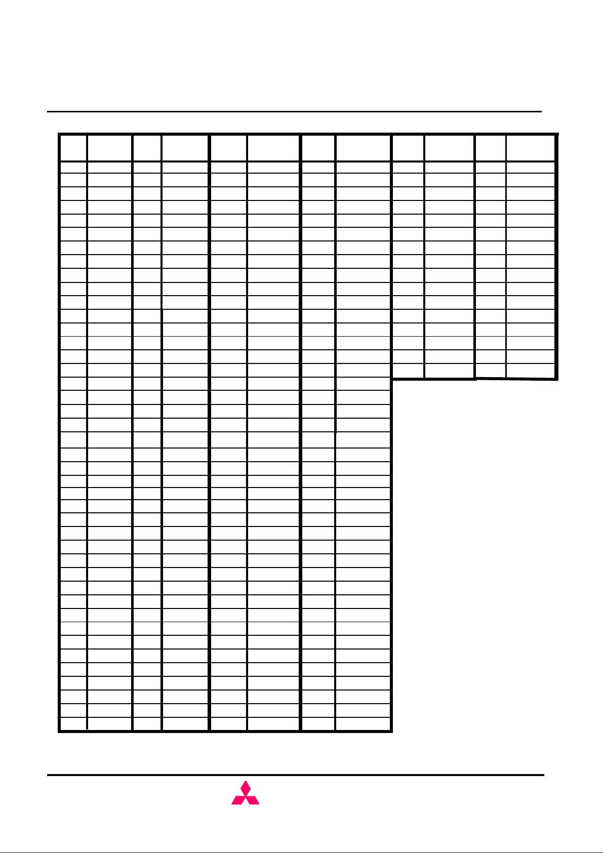
PIN CONFIGURATION
PIN
NO.
PIN
NAME
1 Vref 2 Vref 85
DQ10
Vdd
39 Vss 40
41 DQ16 42
43 DQ17 44
45 Vdd 46
47 DQS2 48
49 DQ18 50
51 Vss 52
53 DQ19 54
55 DQ24 56
57 Vdd 58
59 DQ25 60
61 DQS3 62
63 Vss 64
65 DQ26 66
67 DQ27 68
69 Vdd 70
71 NC 72
73 NC 74
75 Vss 76
77 NC 78
79 NC 80
81 Vdd 82
PIN
NO.
30
PIN
NAME
Vss
DQ4
DQ5
Vdd
DM0
DQ6
Vss
DQ7
DQ12
DQ13
DM1
Vss
DQ14
DQ15
Vdd
Vdd
Vss
Vss
DQ20
DQ21
Vdd
DM2
DQ22
Vss
DQ23
DQ28
Vdd
DQ29
DM3
Vss
DQ30
DQ31
Vdd
NC
NC
Vss
NC
NC
Vdd
NC
PIN
NO.
103
105 10621 Vdd
107 10823 DQ9 24
109 11025 DQS1 26
111 11227 Vss 28
113 11429
115 11631 DQ11 32
117 11833 34
119 12035 CK0 36
121 12237 /CK0 38
123
125
127
129
131
133
135
137
139
141
143
145
147
149
151
153
155
157
159
161
163
165
16783 NC 84
PIN
NAME
NC
Vss
CK2
/CK2
Vdd
CKE1
NC
A12
A9
Vss
A7
A5
A3
A1
Vdd
A10/AP
BA0
/WE
/S0
NC
Vss
DQ32
DQ33
Vdd
DQS4
DQ34
Vss
DQ35
DQ40
Vdd
DQ41
DQS5
Vss
DQ42
DQ43
Vdd
Vdd
Vss
Vss
DQ48
DQ49
Vdd
MH32D64AKQJ-75,-10
PIN
NO.
86 169
883 Vss 4 87
905 DQ0 6 89
927 DQ1 8 91
949 Vdd 10 93
9611 DQS0 12 95
9813 DQ2 14 97
10015 Vss 16 99
10217 DQ3 18 101
10419 DQ8 20
124
126
128
130
132
134
136
138
140
142
144
146
148
150
152
154
156
158
160
162
164
166
168
PIN
NAME
NC
Vss
Vss
Vdd
Vdd
CKE0
NC
A11
A8
Vss
A6
A4
A2
A0
Vdd
BA1
/RAS
/CAS
/S1
NC
Vss
DQ36
DQ37
Vdd
DM4
DQ38
Vss
DQ39
DQ44
Vdd
DQ45
DM5
Vss
DQ46
DQ47
Vdd
/CK1
CK1
Vss
DQ52
DQ53
Vdd
PIN
NO.
171
173
175
177
179
181
183
185
187
189
191
193
195
197
199
PIN
NAME
DQS6
DQ50
Vss
DQ51
DQ56
Vdd
DQ57
DQS7
Vss
DQ58
DQ5922
Vdd
SDA
SCL
VddSPD
VddID
NC: No Connect
MITSUBISHI LSIs
PIN
NO.
170
172
174
176
178
180
182
184
186
188
190
192
194
196
198
200
PIN
NAME
DM6
DQ54
Vss
DQ55
DQ60
Vdd
DQ61
DM7
Vss
DQ62
DQ63Vdd
Vdd
SA0
SA1
SA2
NC
MIT-DS-0422-0.0
MITSUBISHI
ELECTRIC
17.May.2001
2
2,147,483,684
-BIT (33,554,432-WORD BY 64-BIT) Double Data Rate Synchronous DRAM Module
Preliminary Spec.
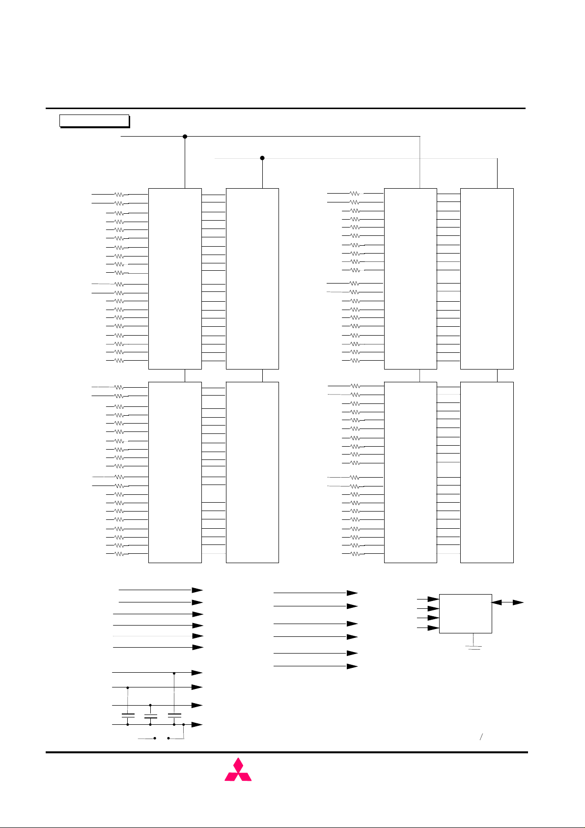
Block Diagram
Some contents are subject to change without notice.
/S0
/S1
MITSUBISHI LSIs
MH32D64AKQJ-75,-10
DQS0 LDQS
DM0
DQ0
DQ1
DQ2
DQ3
DQ4
DQ5
DQ6
DQ7
DQS1 UDQS
DM1
DQ8
DQ9
DQ10
DQ11
DQ12
DQ13
DQ14
DQ15
DQS2 LDQS
DM2
DQ16
DQ17
DQ18
DQ19
DQ20
DQ21
DQ22
DQ23
DQS3 UDQS
DM3
DQ24
DQ25
DQ26
DQ27
DQ28
DQ29
DQ30
DQ31
22Ω
LDM
I/O 0
I/O 1
I/O 2
I/O 3
I/O 4
I/O 5
I/O 6
I/O 7
UDM
I/O 8
I/O 9
I/O 10
I/O 11
I/O 12
I/O 13
I/O 14
I/O 15
LDM
I/O 0
I/O 1
I/O 2
I/O 3
I/O 4
I/O 5
I/O 6
I/O 7
UDM
I/O 8
I/O 9
I/O 10
I/O 11
I/O 12
I/O 13
I/O 14
I/O 15
/S
D0
/S
D1
LDQS
LDM
I/O 0
I/O 1
I/O 2
I/O 3
I/O 4
I/O 5
I/O 6
I/O 7
UDQS
UDM
I/O 8
I/O 9
I/O 10
I/O 11
I/O 12
I/O 13
I/O 14
I/O 15
LDQS
LDM
I/O 0
I/O 1
I/O 2
I/O 3
I/O 4
I/O 5
I/O 6
I/O 7
UDQS
UDM
I/O 8
I/O 9
I/O 10
I/O 11
I/O 12
I/O 13
I/O 14
I/O 15
/S
D4
/S
D5
DQS4
DM4 LDM
DQ32
DQ33
DQ34
DQ35
DQ36
DQ37
DQ38
DQ39
DQS5 UDQS
DM5
DQ40
DQ41
DQ42
DQ43
DQ44
DQ45
DQ46
DQ47
DQS6 LDQS
DM6
DQ48
DQ49
DQ50
DQ51
DQ52
DQ53
DQ54
DQ55
DQS7
DM7
DQ56
DQ57
DQ58
DQ59
DQ60
DQ61
DQ62
DQ63
LDQS
LDM
I/O 0
I/O 1
I/O 2
I/O 3
I/O 4
I/O 5
I/O 6
I/O 7
UDM
I/O 8
I/O 9
I/O 10
I/O 11
I/O 12
I/O 13
I/O 14
I/O 15
LDM
I/O 0
I/O 1
I/O 2
I/O 3
I/O 4
I/O 5
I/O 6
I/O 7
UDQS
UDM
I/O 8
I/O 9
I/O 10
I/O 11
I/O 12
I/O 13
I/O 14
I/O 15
/S
D2
/S
/S /S
D3
LDQS
I/O 0
I/O 1
I/O 2
I/O 3
I/O 4
I/O 5
I/O 6
I/O 7
UDQS
UDM
I/O 8
I/O 9
I/O 10
I/O 11
I/O 12
I/O 13
I/O 14
I/O 15
LDQS
LDM
I/O 0
I/O 1
I/O 2
I/O 3
I/O 4
I/O 5
I/O 6
I/O 7
UDQS
UDM
I/O 8
I/O 9
I/O 10
I/O 11
I/O 12
I/O 13
I/O 14
I/O 15
/S
D6
D7
CKE0
CKE1
/RAS
/CAS
/WE
BA0,BA1,A<12:0>
VddSPD
Vref
Vdd
Vss
VddID
MIT-DS-0422-0.0
D0 - D3
D4 - D7
D0 - D7
D0 - D7
D0 - D7
D0 - D7
SPD
D0 - D7
D0 - D7
D0 - D7
CK0
/CK0
CK1
/CK1
CK2
/CK2
MITSUBISHI
ELECTRIC
4loads
4loads
0loads
SERIAL PD
SCL
SA0
SA1
SA2
NOTE: DQ wiring may differ from that
described in this drawing; however
DQ/DM/DQS relationships are
maintained as shown.
Vdd ID strap connections:
(for memory device Vdd, VddQ)
Strap out (open): Vdd=VddQ
Strap in (closed): Vdd=VddQ
A0
A1
A2
WP
17.May.2001
3
SDA

2,147,483,684
-BIT (33,554,432-WORD BY 64-BIT) Double Data Rate Synchronous DRAM Module
Preliminary Spec.
PIN FUNCTION
Bank Address: BA0-1 specifies one of four banks in SDRAM to which a command
Data Input/Output: Data bus
SYMBOL
DESCRIPTION
Some contents are subject to change without notice.
TYPE
Clock: CK0-2 and /CK0-2 are differential clock inputs. All address and control
CK0-2,/CK0-2 Input
CKE0-1
Input
input signals are sampled on the crossing of the positive edge of CK0-2 and
negative edge of /CK0-2. Output (read) data is referenced to the crossings of
CK0-2 and /CK0-2 (both directions of crossing).
Clock Enable: CKE0-1 controls internal clock. When CKE0-1 is low, internal
clock for the following cycle is ceased. CKE0-1 is also used to select auto /
self refresh. After self refresh mode is started, CKE0-1 becomes
asynchronous input. Self refresh is maintained as long as CKE0-1 is low.
MITSUBISHI LSIs
MH32D64AKQJ-75,-10
/S0-1
Input
/RAS, /CAS, /WE Input
A0-12 Input
BA0-1 Input
DQ 0-64 Input / Output
DQS0-7
DM0-7
Input / Output
Input
Vdd, Vss Power Supply
Vddspd
Power Supply Power Supply for SPD
Vref Input
Chip Select : When /S0-1 is high, any command means No Operation.
Combination of /RAS, /CAS, /WE defines basic commands.
A0-11 specify the Row / Column Address in conjunction with BA0,1. The Row
Address is specified by A0-12. The Column Address is specified by A0-8.
A10 is also used to indicate precharge option. When A10 is high at a read / write
command, an auto precharge is performed. When A10 is high at a precharge
command, all banks are precharged.
is applied. BA0-1 must be set with ACT, PRE, READ, WRITE commands.
Data Strobe: Output with read data, input with write data. Edge-aligned with read
data, centered in write data. Used to capture write data.
Input Data Mask: DM is an input mask signal for write data. Input data is masked when DM0-7 is
sampled HIGH along with that input data during a WRITE access. DM0-7 is sampled on both
edges of DQS0-7. Although DM pins are input only, the DM0-7 loading matches the DQ0-63 and
DQS0-7 loading.
Power Supply for the memory array and peripheral circuitry.
SSTL_2 reference voltage.
SDA
SCL
SA0-2
VddID
MIT-DS-0422-0.0
Input / Output
Input / Output
Input
Output
This is a bidirectional pin used to transfer data into or out of the SPD EEPROM.
A resistor must be connected to Vdd to act as a pullup.
This signal is used to clock data into and out of the SPD EEPROM. A resistor
may be connected from the SCL to Vdd to act as a pullup.
Address pins used to select the Serial Presence Detect.
Vdd identification flag
MITSUBISHI
ELECTRIC
17.May.2001
4

2,147,483,684
-BIT (33,554,432-WORD BY 64-BIT) Double Data Rate Synchronous DRAM Module
Preliminary Spec.
BASIC FUNCTIONS
The MH32D64AKQJ provides basic functions, bank (row) activate, burst read / write, bank (row)
burst read (auto-precharge,
READA
)
WRITE command starts burst write to the active bank indicated by BA. Total data length to be
the burst write (auto-precharge,
WRITEA
).
PRE command deactivates the active bank indicated by BA. This command also terminates
(precharge all,
PREA
).
generated internally. After this command, the banks are precharged automatically.
Some contents are subject to change without notice.
MITSUBISHI LSIs
MH32D64AKQJ-75,-10
precharge, and auto / self refresh. Each command is defined by control signals of /RAS, /CAS
and /WE at CLK rising edge. In addition to 3 signals, /CS ,CKE and A10 are used as chip
select, refresh option, and precharge option, respectively. To know the detailed definition of
commands, please see the command truth table.
/CK0
CK0
/S0
Chip Select : L=select, H=deselect
/RAS
/CAS
/WE
CKE0
A10
Command
Command
Command
Refresh Option @refresh command
Precharge Option @precharge or read/write command
define basic commands
Activate (ACT) [/RAS =L, /CAS =/WE =H]
ACT command activates a row in an idle bank indicated by BA.
Read (READ) [/RAS =H, /CAS =L, /WE =H]
READ command starts burst read from the active bank indicated by BA. First output data
appears after /CAS latency. When A10 =H at this command, the bank is deactivated after the
Write (WRITE) [/RAS =H, /CAS =/WE =L]
written is set by burst length. When A10 =H at this command, the bank is deactivated after
Precharge (PRE) [/RAS =L, /CAS =H, /WE =L]
burst read /write operation. When A10 =H at this command, all banks are deactivated
Auto-Refresh (REFA) [/RAS =/CAS =L, /WE =CKE0 =H]
REFA command starts auto-refresh cycle. Refresh address including bank address are
MIT-DS-0422-0.0
MITSUBISHI
17.May.2001
ELECTRIC
5
2,147,483,684
-BIT (33,554,432-WORD BY 64-BIT) Double Data Rate Synchronous DRAM Module
Preliminary Spec.
COMMAND TRUTH TABLE
Some contents are subject to change without notice.
MITSUBISHI LSIs
MH32D64AKQJ-75,-10
CKE
COMMAND MNEMONIC
Deselect DESEL H X H X X X X X X
No Operation NOP H X L H H H X X X
Row Address Entry &
Bank Activate
Single Bank Precharge PRE H H L L H L V L X
Precharge All Banks PREA H H L L H L H X
Column Address Entry
& Write
Column Address Entry
& Write with
Auto-Precharge
Column Address Entry
& Read
ACT H H L L H H V V V
WRITE H H L H L L V L V
WRITEA H H L H L L V H V
READ H H L H L H V L V
n-1
CKE
n
/S /RAS /CAS /WE BA0,1
A10
/AP
X
A0-9,
11
note
Column Address Entry
& Read with
Auto-Precharge
Auto-Refresh
Self-Refresh Entry REFS H L L L L H X X X
Self-Refresh Exit REFSX
Burst Terminate TERM H H L H H L X X X
Mode Register Set MRS H H L L L L L L V
H=High Level, L=Low Level, V=Valid, X=Don't Care, n=CLK cycle number
NOTE:
1. Applies only to read bursts with autoprecharge disabled; this command is undefined (and should
not be used) for read bursts with autoprecharge enabled, and for write bursts.
2. BA0-BA1 select either the Base or the Extended Mode Register (BA0 = 0, BA1 = 0 selects Mode
Register; BA0 = 1, BA1 = 0 selects Extended Mode Register; other combinations of BA0-BA1 are
reserved; A0-A11 provide the op-code to be written to the selected Mode Register.
READA H H L H L H V H V
REFA H H L L L H X X X
L H H X X X X X X
L H L H H H X X X
1
2
MIT-DS-0422-0.0
MITSUBISHI
ELECTRIC
17.May.2001
6
2,147,483,684
-BIT (33,554,432-WORD BY 64-BIT) Double Data Rate Synchronous DRAM Module
Preliminary Spec.
Notes
Some contents are subject to change without notice.
MH32D64AKQJ-75,-10
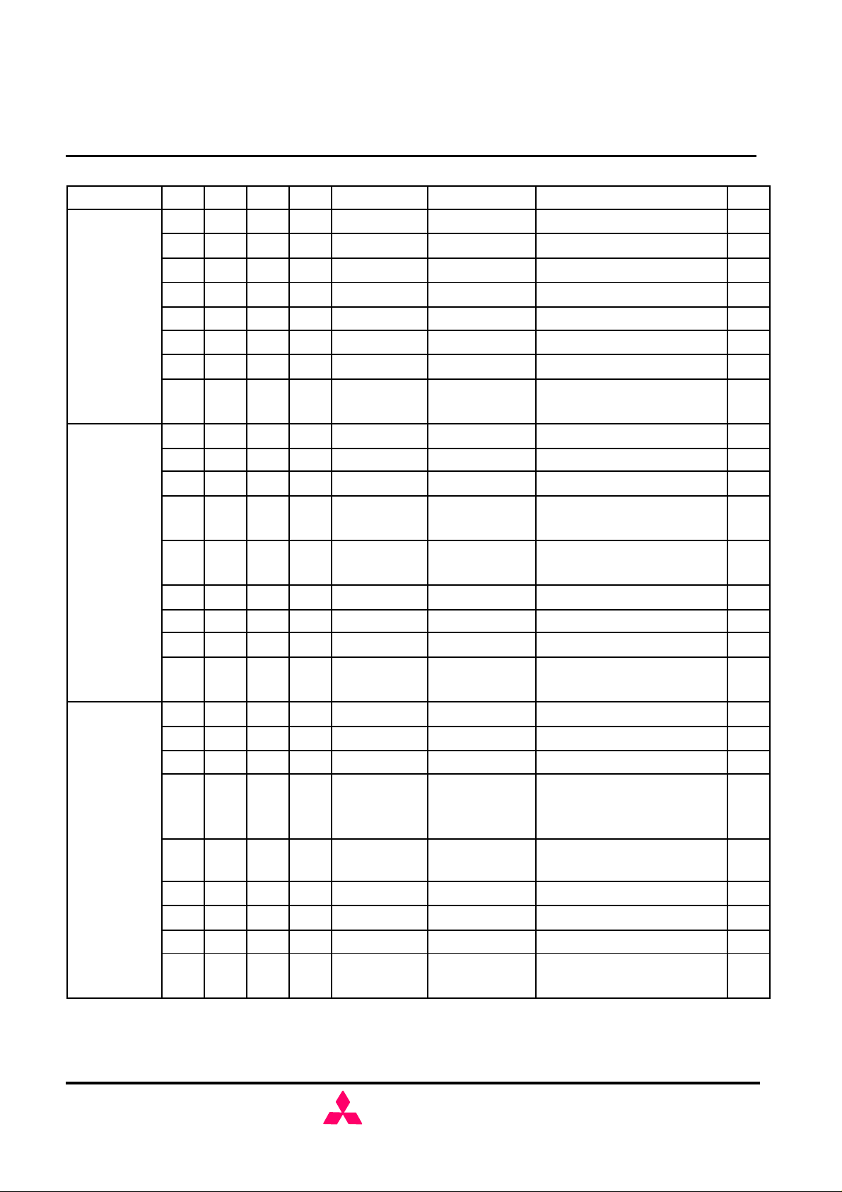
FUNCTION TRUTH TABLE
Current State /S /RAS /CAS /WE Address Command Action
IDLE H X X X X DESEL NOP
L H H H X NOP NOP
L H H L BA TERM ILLEGAL
MITSUBISHI LSIs
2
L H L X BA, CA, A10 READ / WRITE ILLEGAL
L L H H BA, RA ACT Bank Active, Latch RA
L L H L BA, A10 PRE / PREA NOP
L L L H X REFA Auto-Refresh
L L L L
ROW ACTIVE H X X X X DESEL NOP
L H H H X NOP NOP
L H H L BA TERM NOP
L H L H BA, CA, A10 READ / READA
L H L L BA, CA, A10
L L H H BA, RA ACT Bank Active / ILLEGAL
L L H L BA, A10 PRE / PREA Precharge / Precharge All
L L L H X REFA ILLEGAL
L L L L
READ
(Auto-
Precharge
Disabled)
H X X X X DESEL NOP (Continue Burst to END)
L H H H X NOP NOP (Continue Burst to END)
L H H L BA TERM Terminate Burst
L H L H BA, CA, A10 READ / READA
L H L L BA, CA, A10
L L H H BA, RA ACT Bank Active / ILLEGAL
Op-Code,
Mode-Add
Op-Code,
Mode-Add
MRS Mode Register Set
Begin Read, Latch CA,
Determine Auto-Precharge
WRITE /
WRITEA
MRS ILLEGAL
WRITE
WRITEA
Begin Write, Latch CA,
Determine Auto-Precharge
Terminate Burst, Latch CA,
Begin New Read, Determine
Auto-Precharge
ILLEGAL
2
4
5
5
2
3
2
L L H L BA, A10 PRE / PREA Terminate Burst, Precharge
L L L H X REFA ILLEGAL
L L L L
MIT-DS-0422-0.0
Op-Code,
Mode-Add
MITSUBISHI
ELECTRIC
MRS ILLEGAL
17.May.2001
7
2,147,483,684
-BIT (33,554,432-WORD BY 64-BIT) Double Data Rate Synchronous DRAM Module
Preliminary Spec.
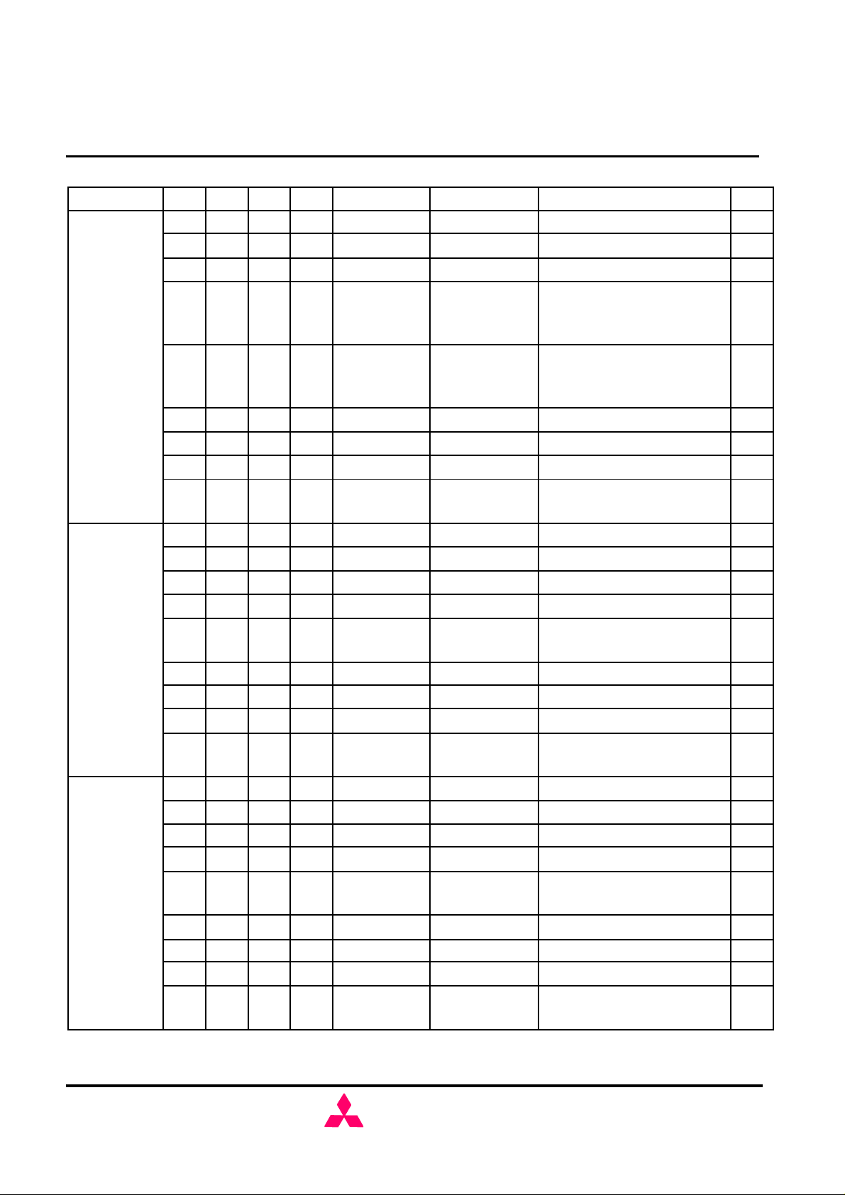
FUNCTION TRUTH TABLE (continued)
Notes
Some contents are subject to change without notice.
MITSUBISHI LSIs
MH32D64AKQJ-75,-10
Current State
WRITE
(Auto-
Precharge
Disabled)
READ with
AUTO
PRECHARGE
/S
/RAS /CAS /WE Address Command Action
H X X X X DESEL NOP (Continue Burst to END)
L H H H X NOP NOP (Continue Burst to END)
L H H L BA TERM ILLEGAL
Terminate Burst, Latch CA,
L H L H BA, CA, A10 READ / READA
L H L L BA, CA, A10
L L H H BA, RA ACT Bank Active / ILLEGAL
L L H L BA, A10 PRE / PREA Terminate Burst, Precharge
L L L H X REFA ILLEGAL
L L L L
H X X X X DESEL NOP (Continue Burst to END)
L H H H X NOP NOP (Continue Burst to END)
L H H L BA TERM ILLEGAL
L H L H BA, CA, A10 READ / READA ILLEGAL
Op-Code,
Mode-Add
WRITE /
WRITEA
MRS ILLEGAL
Begin Read, Determine AutoPrecharge
Terminate Burst, Latch CA,
Begin Write, Determine AutoPrecharge
3
3
2
WRITE with
AUTO
PRECHARGE
L H L L BA, CA, A10
L L H H BA, RA ACT Bank Active / ILLEGAL
L L H L BA, A10 PRE / PREA PRECHARGE/ILLEGAL
L L L H X REFA ILLEGAL
L L L L
H X X X X DESEL NOP (Continue Burst to END)
L H H H X NOP NOP (Continue Burst to END)
L H H L BA TERM ILLEGAL
L H L H BA, CA, A10 READ / READA ILLEGAL
L H L L BA, CA, A10
L L H H BA, RA ACT Bank Active / ILLEGAL
L L H L BA, A10 PRE / PREA PRECHARGE/ILLEGAL
L L L H X REFA ILLEGAL
L L L L
Op-Code,
Mode-Add
Op-Code,
Mode-Add
WRITE /
WRITEA
MRS ILLEGAL
WRITE /
WRITEA
MRS ILLEGAL
ILLEGAL
ILLEGAL
2
2
2
2
MIT-DS-0422-0.0
MITSUBISHI
ELECTRIC
17.May.2001
8
2,147,483,684
-BIT (33,554,432-WORD BY 64-BIT) Double Data Rate Synchronous DRAM Module
Preliminary Spec.
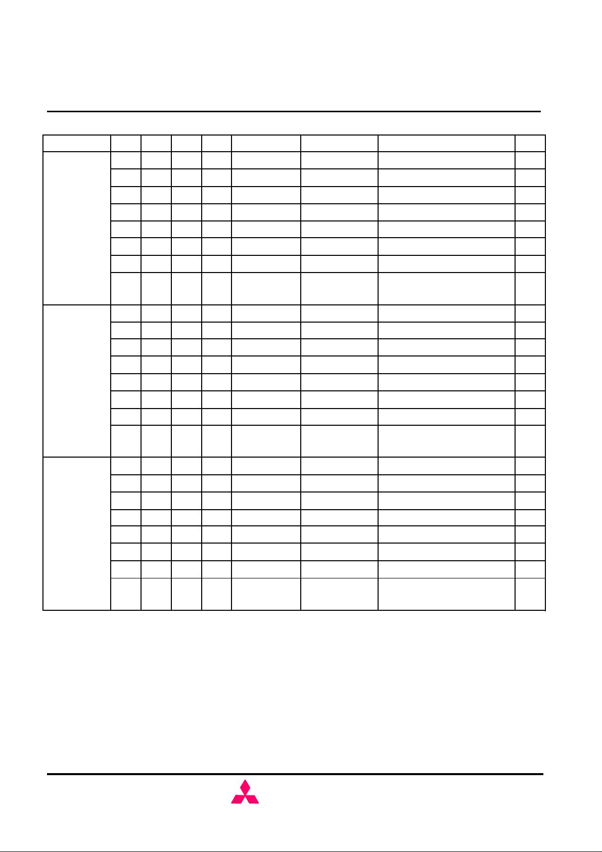
FUNCTION TRUTH TABLE (continued)
Notes
Some contents are subject to change without notice.
MH32D64AKQJ-75,-10
Current State /S /RAS /CAS /WE Address Command Action
MITSUBISHI LSIs
PRE -
CHARGING
ROW
ACTIVATING
H X X X X DESEL NOP (Idle after tRP)
L H H H X NOP NOP (Idle after tRP)
L H H L BA TERM ILLEGAL
L H L X BA, CA, A10 READ / WRITE ILLEGAL
L L H H BA, RA ACT ILLEGAL
L L H L BA, A10 PRE / PREA NOP (Idle after tRP)
L L L H X REFA ILLEGAL
L L L L
H X X X X DESEL NOP (Row Active after tRCD)
L H H H X NOP NOP (Row Active after tRCD)
L H H L BA TERM ILLEGAL
L H L X BA, CA, A10 READ / WRITE ILLEGAL
L L H H BA, RA ACT ILLEGAL
L L H L BA, A10 PRE / PREA ILLEGAL
L L L H X REFA ILLEGAL
L L L L
Op-Code,
Mode-Add
Op-Code,
Mode-Add
MRS ILLEGAL
MRS ILLEGAL
2
2
2
4
2
2
2
2
WRITE RECOVERING
H X X X X DESEL NOP
L H H H X NOP NOP
L H H L BA TERM ILLEGAL
L H L X BA, CA, A10 READ / WRITE ILLEGAL
L L H H BA, RA ACT ILLEGAL
L L H L BA, A10 PRE / PREA ILLEGAL
L L L H X REFA ILLEGAL
L L L L
Op-Code,
Mode-Add
MRS ILLEGAL
2
2
2
2
MIT-DS-0422-0.0
MITSUBISHI
ELECTRIC
17.May.2001
9
2,147,483,684
-BIT (33,554,432-WORD BY 64-BIT) Double Data Rate Synchronous DRAM Module
Preliminary Spec.
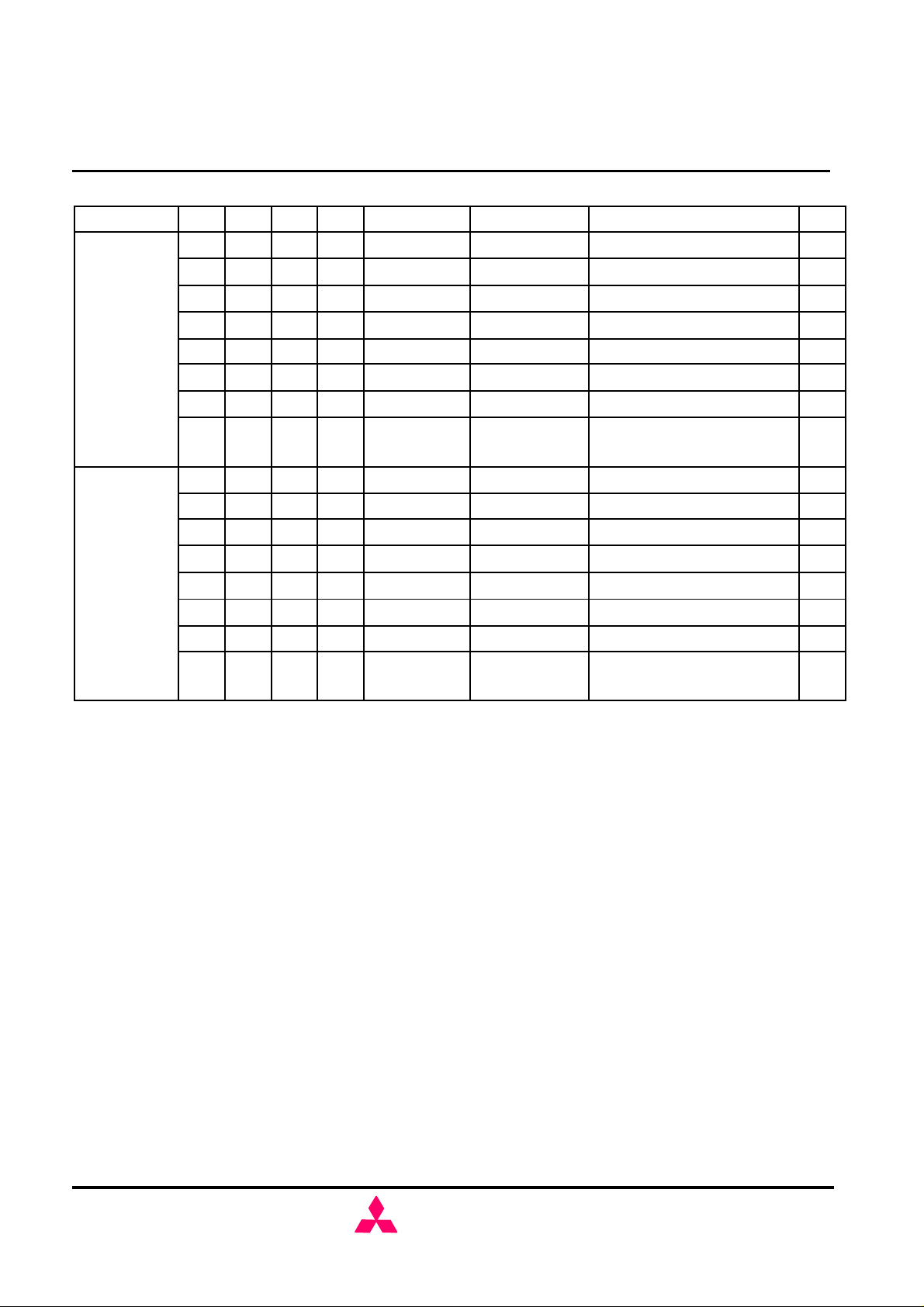
FUNCTION TRUTH TABLE (continued)
Notes
Some contents are subject to change without notice.
MH32D64AKQJ-75,-10
Current State /S /RAS /CAS /WE Address Command Action
MITSUBISHI LSIs
RE-
FRESHING
MODE
REGISTER
SETTING
H X X X X DESEL NOP (Idle after tRC)
L H H H X NOP NOP (Idle after tRC)
L H H L BA TERM ILLEGAL
L H L X BA, CA, A10 READ / WRITE ILLEGAL
L L H H BA, RA ACT ILLEGAL
L L H L BA, A10 PRE / PREA ILLEGAL
L L L H X REFA ILLEGAL
L L L L
H X X X X DESEL NOP (Idle after tRSC)
L H H H X NOP NOP (Idle after tRSC)
L H H L BA TERM ILLEGAL
L H L X BA, CA, A10 READ / WRITE ILLEGAL
L L H H BA, RA ACT ILLEGAL
L L H L BA, A10 PRE / PREA ILLEGAL
L L L H X REFA ILLEGAL
L L L L
Op-Code,
Mode-Add
Op-Code,
Mode-Add
MRS ILLEGAL
MRS ILLEGAL
ABBREVIATIONS:
H=High Level, L=Low Level, X=Don't Care
BA=Bank Address, RA=Row Address, CA=Column Address, NOP=No Operation
NOTES:
1. All entries assume that CKE was High during the preceding clock cycle and the current clock cycle.
2. ILLEGAL to bank in specified state; function may be legal in the bank indicated by BA, depending on the state of
that bank.
3. Must satisfy bus contention, bus turn around, write recovery requirements.
4. NOP to bank precharging or in idle state. May precharge bank indicated by BA.
5. ILLEGAL if any bank is not idle.
ILLEGAL = Device operation and/or data-integrity are not guaranteed.
MIT-DS-0422-0.0
MITSUBISHI
ELECTRIC
17.May.2001
10
2,147,483,684
-BIT (33,554,432-WORD BY 64-BIT) Double Data Rate Synchronous DRAM Module
Preliminary Spec.
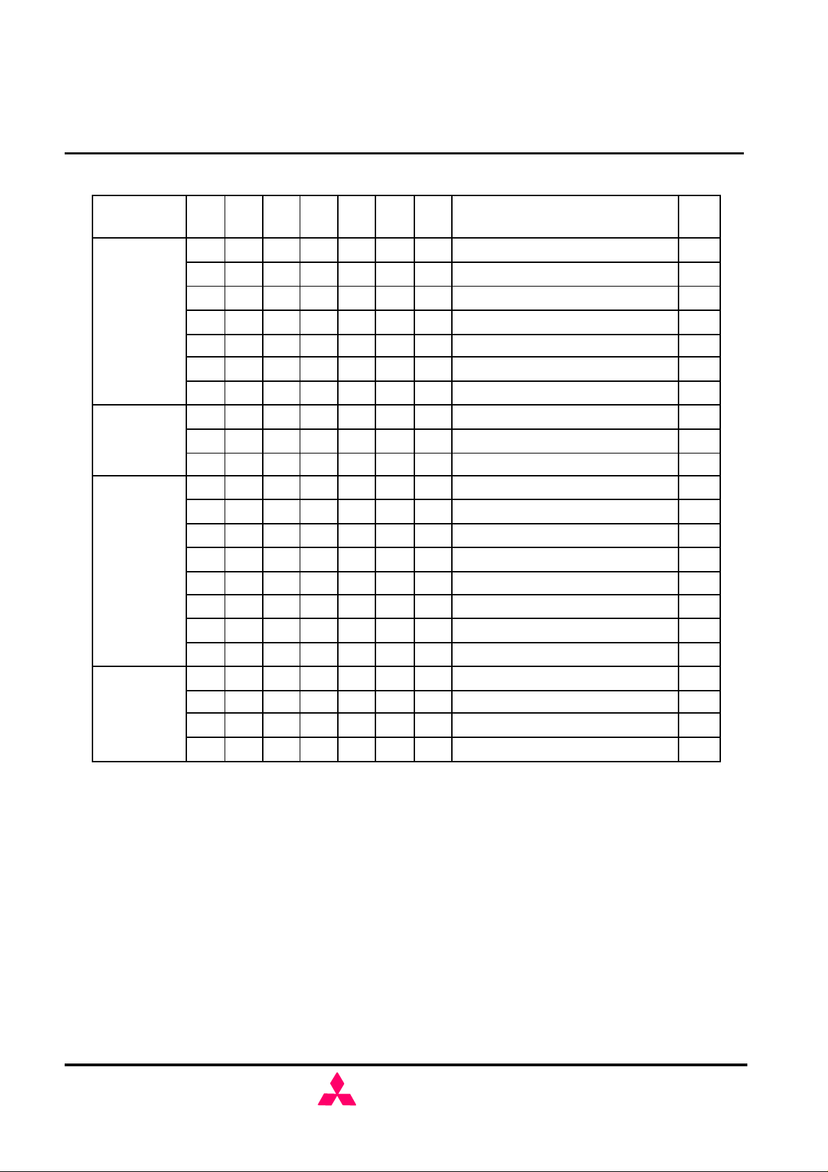
FUNCTION TRUTH TABLE for CKE
asynchronously
Notes
Some contents are subject to change without notice.
CKE0
Current State
SELF-
REFRESH
POWER
DOWN
ALL BANKS
IDLE
CKE0
n-1
H X X X X X X INVALID
L H H X X X X Exit Self-Refresh (Idle after tRC)
L H L H H H X Exit Self-Refresh (Idle after tRC)
L H L H H L X ILLEGAL
L H L H L X X ILLEGAL
L H L L X X X ILLEGAL
L L X X X X X NOP (Maintain Self-Refresh)
H X X X X X X INVALID
L H X X X X X Exit Power Down to Idle
L L X X X X X NOP (Maintain Self-Refresh)
H H X X X X X Refer to Function Truth Table
H L L L L H X Enter Self-Refresh
H L H X X X X Enter Power Down
H L L H H H X Enter Power Down
H L L H H L X ILLEGAL
H L L H L X X ILLEGAL
H L L L X X X ILLEGAL
L X X X X X X Refer to Current State =Power Down
/S0 /RAS /CAS
n
MITSUBISHI LSIs
MH32D64AKQJ-75,-10
/WE Add Action
1
1
1
1
1
1
1
2
2
2
2
2
2
2
2
ANY STATE
other than
listed above
ABBREVIATIONS:
H=High Level, L=Low Level, X=Don't Care
NOTES:
1. CKE Low to High transition will re-enable CK0 and other inputs
. A minimum setup time must be satisfied before any command other than EXIT.
2. Power-Down and Self-Refresh can be entered only from the All Banks Idle State.
3. Must be legal command.
MIT-DS-0422-0.0
H H X X X X X Refer to Function Truth Table
H L X X X X X Begin CLK Suspend at Next Cycle
L H X X X X X Exit CLK Suspend at Next Cycle
L L X X X X X Maintain CLK Suspend
MITSUBISHI
ELECTRIC
3
3
17.May.2001
11
2,147,483,684
-BIT (33,554,432-WORD BY 64-BIT) Double Data Rate Synchronous DRAM Module
Preliminary Spec.
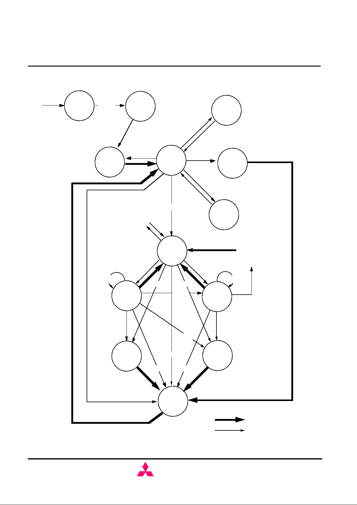
SIMPLIFIED STATE DIAGRAM
REGISTER
Some contents are subject to change without notice.
MITSUBISHI LSIs
MH32D64AKQJ-75,-10
POWER
APPLIED
POWER
ON
PREA
MODE
SET
PRE
CHARGE
ALL
MRS
MRS
Active
Power
Down
CKEH
CKEL
ACTIVE
IDLE
ACT
ROW
REFS
CKEH
REFSX
REFA
CKEL
SELF
REFRESH
AUTO
REFRESH
POWER
DOWN
BURST
STOP
WRITE READ
WRITE READ
WRITEA
WRITE
WRITEA READA
PRE PRE
PRE
READA
READ
READA
READ
READAWRITEA
PRE
CHARGE
TERM
Automatic Sequence
Command Sequence
MIT-DS-0422-0.0
MITSUBISHI
ELECTRIC
17.May.2001
12
 Loading...