

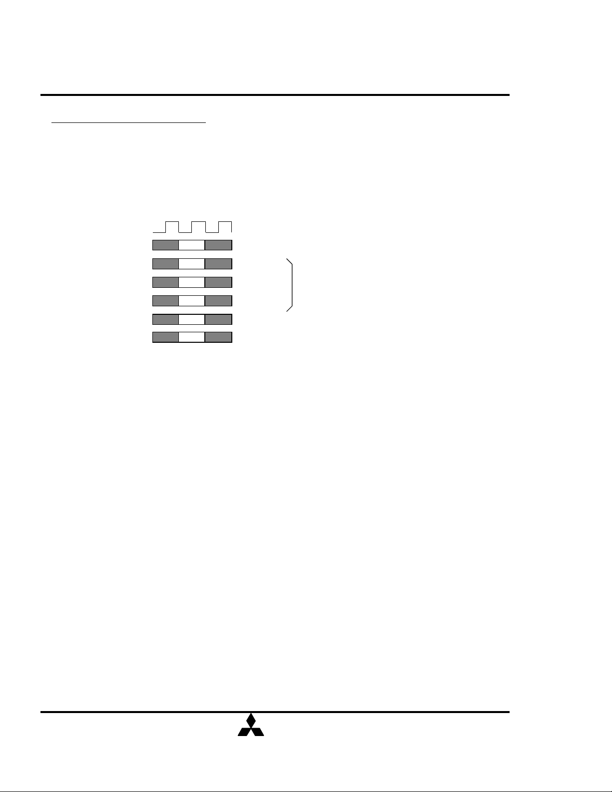
Preliminary Spec.
Some contents are subject to change without notice.
MH1S64CWXTJ-12,-15,-1539
DESCRIPTION
The MH1S64CWXTJ is 1048576-word by 64-bit
Synchronous DRAM module. This consists of four
industry standard 1Mx16 Synchronous DRAMs in
TSOP and one industory standard EEPROM in
TSSOP.
The mounting of TSOP on a card edge Dual Inline
package provides any application where high
densities and large quantities of memory are
required.
This is a socket type - memory modules, suitable for
easy interchange or addition of modules.
FEATURES
Frequency
-12
83MHz
-15 67MHz 9.5ns (CL=2)
CLK Access Time
(Component SDRAM)
8ns(CL=3)
MITSUBISHI LSIs
67108864-BIT (1048576-WORD BY 64-BIT)SynchronousDRAM
85pin
94pin
95pin
1pin
10pin
11pin
-1539 67MHz
Utilizes industry standard 1M x 16 Synchronous DRAMs
TSOP and industry standard EEPROM in TSSOP
168-pin (84-pin dual in-line package)
9ns (CL=3)
single 3.3V±0.3V power supply
Clock frequency 83MHz/67MHz
Fully synchronous operation referenced to clock rising
edge
Dual bank operation controlled by BA(Bank Address)
/CAS latency- 1/2/3(programmable)
Burst length- 1/2/4/8(programmable)
Burst type- sequential / interleave(programmable)
Column access - random
Auto precharge / All bank precharge controlled by A10
Auto refresh and Self refresh
4096 refresh cycle /64ms
LVTTL Interface
APPLICATION
main memory or graphic memory in computer systems
124pin
125pin
Back side
168pin
Front side
40pin
41pin
84pin
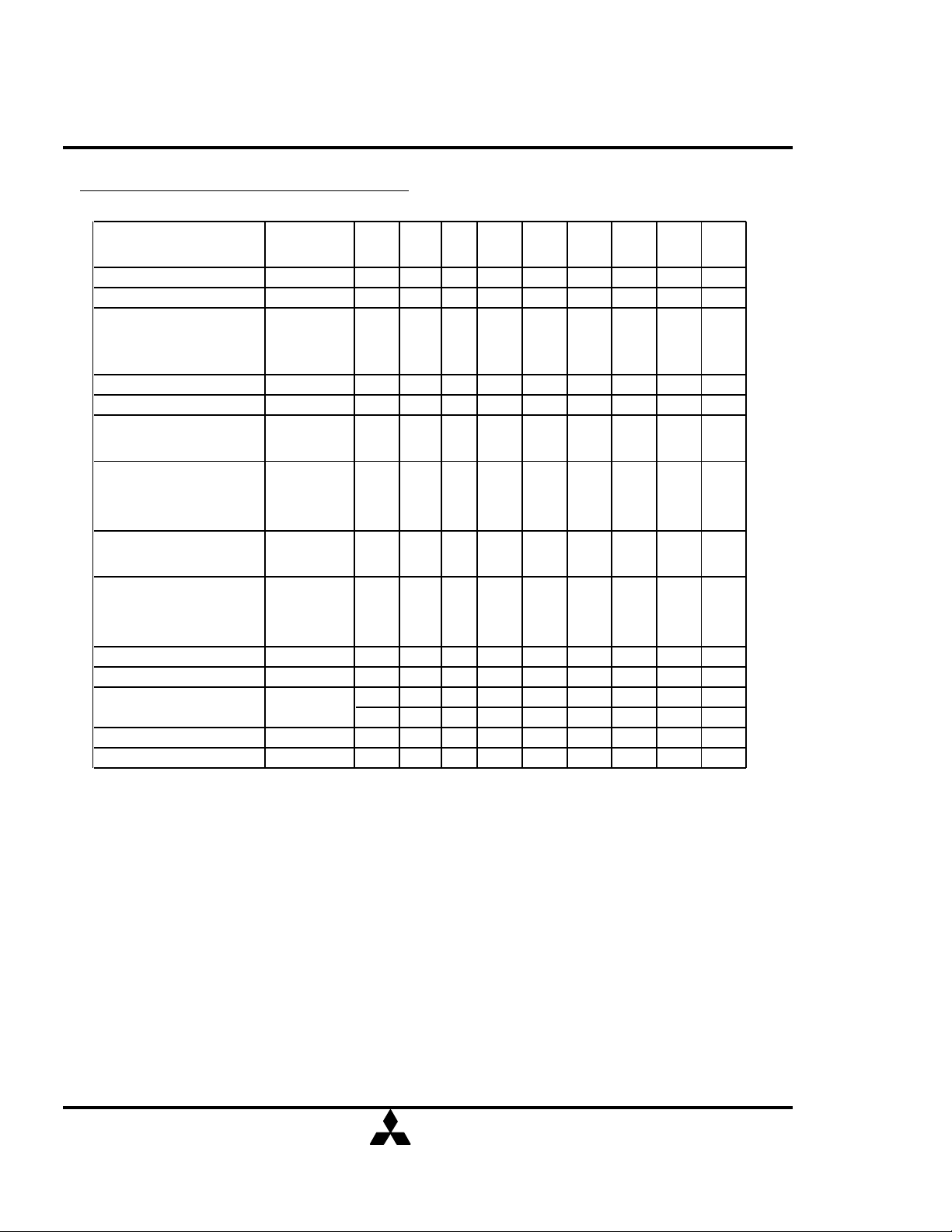
SPD table
Byte No.
MH1S64CWXTJ-12
MH1S64CWXTJ-15
MH1S64CWXTJ-1539
MIT-DS-0064-0.2
0 1 2 3 4 5 6 7 8 9
80 08 04 0C 08 01 40 00 01 C0
80 08 04 0C 08 01 40 00 01 F0 95 00 80
80 08 04 0C 08 01 40 00 01 F0
10 11 12
80
00 80
90
00 80
MITSUBISHI
ELECTRIC
( / 45 )
1
13
00
00
00
14
15
06
01
06
01
04 01
16
17
18
19
20
126
05
02
06
01
01
83
05
02
06
01
01
66
05 02 04 01 01 66
Oct.28.1996
127
06
06
04
Preliminary Spec.
Some contents are subject to change without notice.
MH1S64CWXTJ-12,-15,-1539
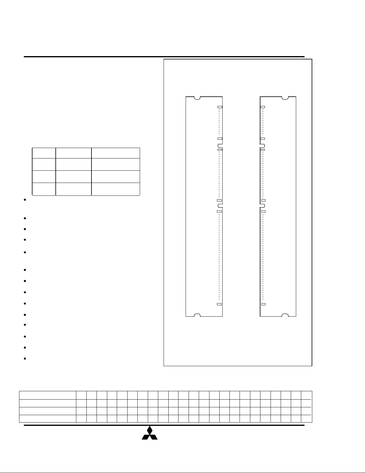
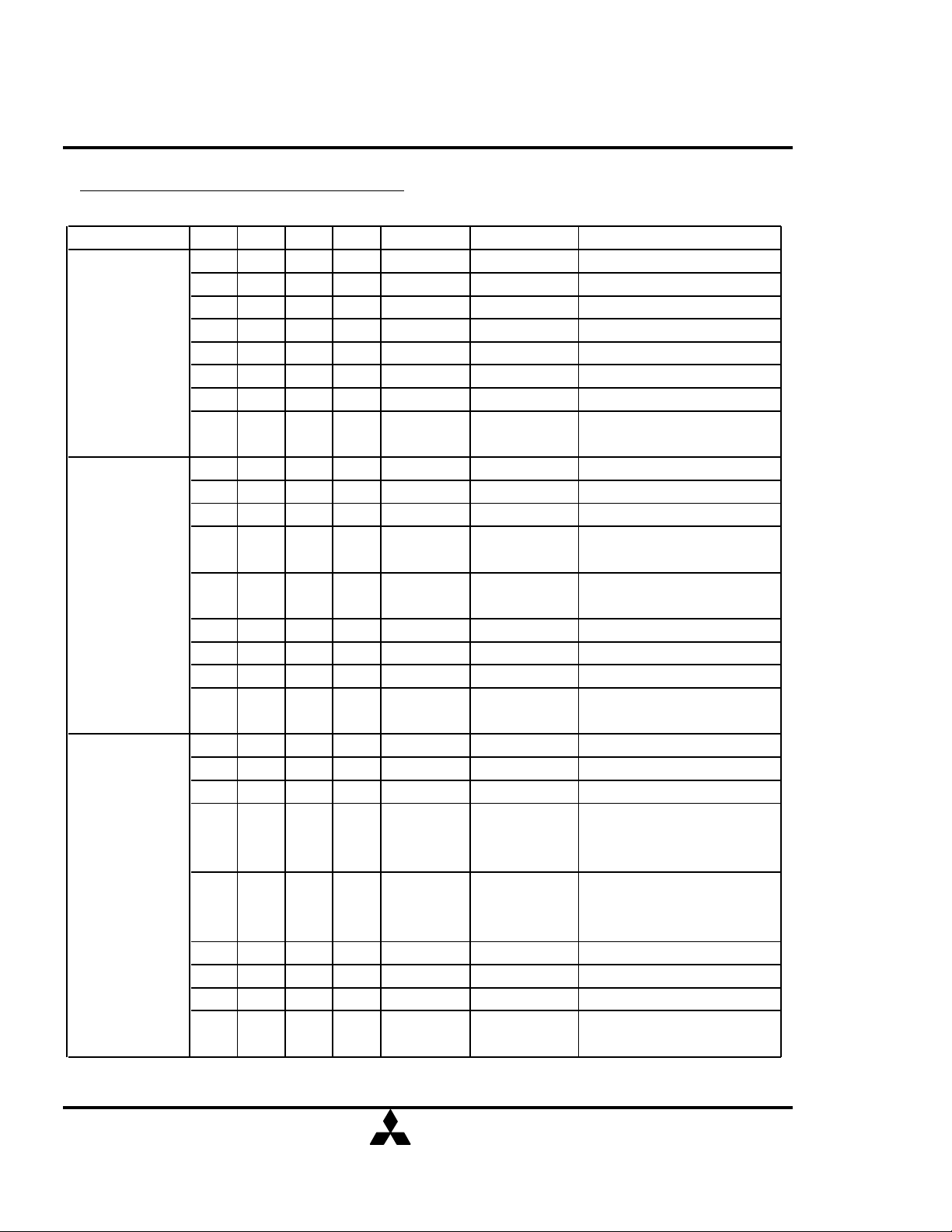
PIN CONFIGURATION
PIN NO. PIN NAME PIN NO. PIN NAME PIN NO. PIN NAME PIN NO. PIN NAME
1
2 DQ0 44 NC
3 DQ1 45 /S2
4 DQ2 46 DQMB2
5 DQ3 47 DQMB3
6 VDD 48 NC
7 DQ4 49 VDD
8 DQ5 50 NC
9 DQ6 51 NC
10 DQ7 52 NC
11 DQ8 53 NC
12
13 DQ9 55 DQ16
14 DQ10 56 DQ17
15 DQ11 57 DQ18
16 DQ12 58 DQ19
17 DQ13 59 VDD
18 VDD 60 DQ20
19 DQ14 61 NC
20 DQ15 62 NC
21 NC 63 NC
22 NC 64 VSS
23 VSS 65 DQ21
24 NC 66 DQ22
25 NC 67 DQ23
26 VDD 68
27
28 DQMB0 70 DQ25
29 DQMB1 71 DQ26
30 /S0 72 DQ27
31 NC 73 VDD
32 VSS 74 DQ28
33 A0 75 DQ29
34 A2 76 DQ30
35 A4 77 DQ31
36 A6 78 VSS
37 A8 79 NC
38
39
40 VDD 82 SDA
41 VDD 83 SCL
42 CK0 84 VDD
VSS
VSS
/WE
A10
NC
43
54 VSS
69 DQ24
80 NC
81 NC
MITSUBISHI LSIs
67108864-BIT (1048576-WORD BY 64-BIT)SynchronousDRAM
VSS 85
86
87
88
89
90
91
92
93
94
95
96
97
98
99
100
101
102
103
104
105
106
107
108
109
VSS 110
111
112
113
114
115
116
117
118
119
120
121
122
123
124
125
126
VSS 127
DQ32 128 CKE
DQ33 129
DQ34 130 DQMB6
DQ35 131 DQMB7
VDD 132
DQ36 133 VDD
DQ37 134 NC
DQ38 135 NC
DQ39 136 NC
DQ40 137 NC
VSS 138 VSS
DQ41 139 DQ48
DQ42 140 DQ49
DQ43 141 DQ50
DQ44 142 DQ51
DQ45 143 VDD
VDD 144 DQ52
DQ46 145 NC
DQ47 146 NC
NC 147 NC
NC 148 VSS
VSS 149 DQ53
NC 150 DQ54
NC 151 DQ55
VDD 152 VSS
/CAS 153 DQ56
DQMB4 154 DQ57
DQMB5 155 DQ58
NC
/RAS 157 VDD
VSS 158 DQ60
A1 159 DQ61
A3 160 DQ62
A5 161 DQ63
A7 162 VSS
A9 163 NC
BA
NC
VDD 166 SA1
NC
NC
156 DQ59
164 NC
165 SA0
167 SA2
168 VDD
VSS
NC
NC
NC = No Connection
MIT-DS-0064-0.2
MITSUBISHI
ELECTRIC
( / 45 )
2
Oct.28.1996
Preliminary Spec.
Some contents are subject to change without notice.
MH1S64CWXTJ-12,-15,-1539
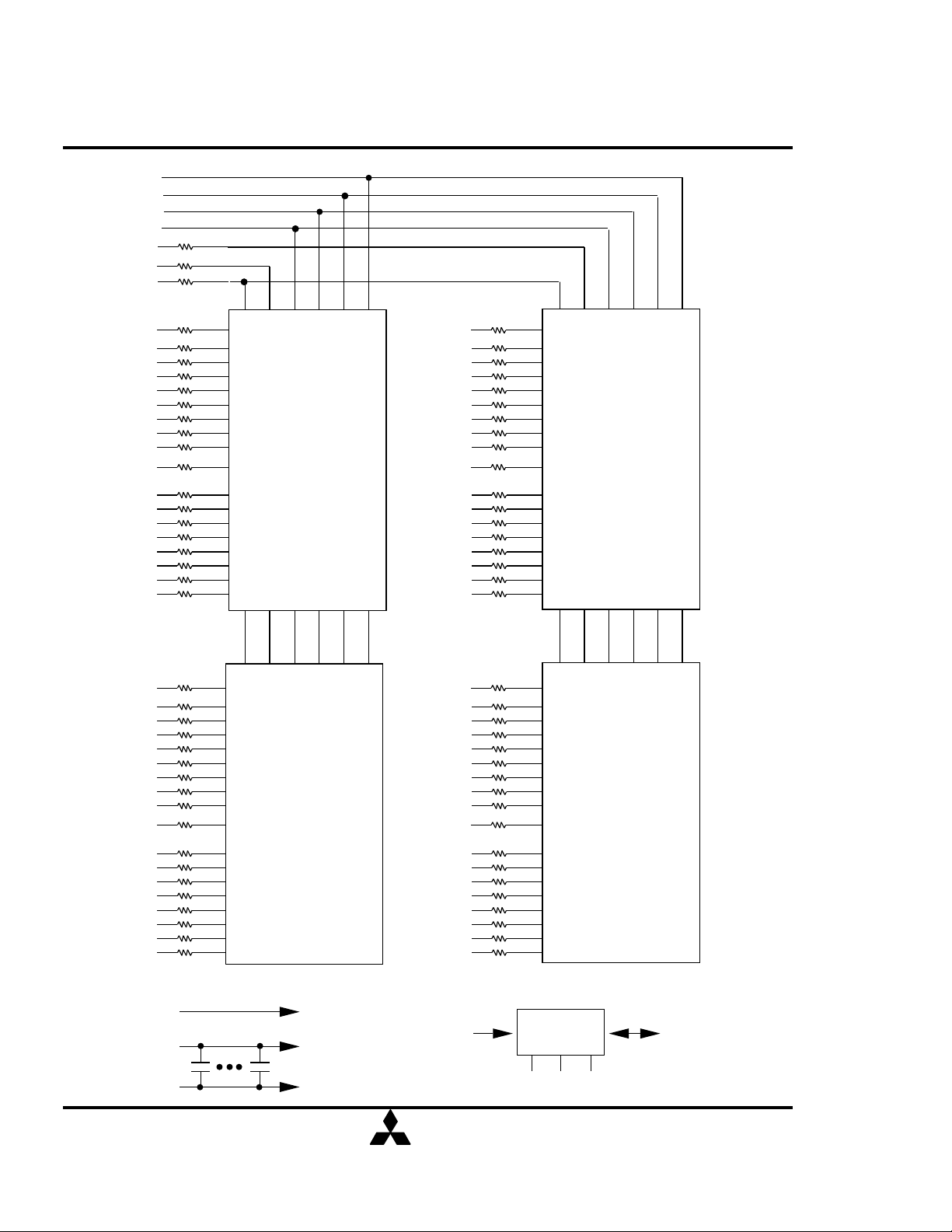
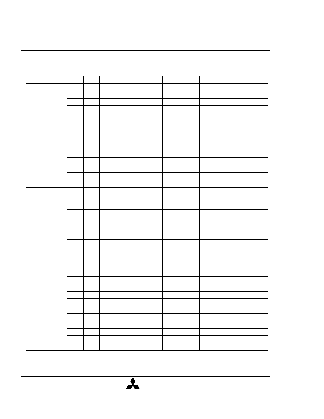
Block Diagram
CKE
/WE
/CAS
/RAS
/S2
/S0
CK0
MITSUBISHI LSIs
67108864-BIT (1048576-WORD BY 64-BIT)SynchronousDRAM
DQMB0
DQ0
DQ1
DQ2
DQ3
DQ4
DQ5
DQ6
DQ7
DQMB4
DQ32
DQ33
DQ34
DQ35
DQ36
DQ37
DQ38
DQ39
DQMB1
DQ8
DQ9
DQ10
DQ11
DQ12
DQ13
DQ14
DQ15
DQMB5
DQ40
DQ41
DQ42
DQ43
DQ44
DQ45
DQ46
DQ47
CLK CS RAS CAS WE CKE
DQML DQML
DQ0~DQ7
DQMU
DQ8~DQ15
CLK CS RAS CAS WE CKE
DQML DQML
DQ0~DQ7
DQMU
DQ8~DQ15
D0
D2
D1
DQMB2
DQ16
DQ17
DQ18
DQ19
DQ20
DQ21
DQ22
DQ23
DQMB6
DQ48
DQ49
DQ50
DQ51
DQ52
DQ53
DQ54
DQ55
DQMB3
DQ24
DQ25
DQ26
DQ27
DQ28
DQ29
DQ30
DQ31
DQMB7
DQ56
DQ57
DQ58
DQ59
DQ60
DQ61
DQ62
DQ63
CLK CS RAS CAS WE CKE
I/O0
I/O1
I/O2
DQ0~DQ7
I/O3
I/O4
I/O5
I/O6
I/O7
DQMU
DQ8~DQ15
CLK CS RAS CAS WE CKE
DQ0~DQ7
DQMU
DQ8~DQ15
D4
D2
D3
BA,A(10:0) D0 to D3
Vcc
Vss
MIT-DS-0064-0.2
D0 to D3
D0 to D3
SCL
MITSUBISHI
ELECTRIC
3
( / 45 )
SERIAL PD
A0 A1 A2
SA0 SA1 SA2
SDA
Oct.28.1996
Preliminary Spec.
Some contents are subject to change without notice.
MH1S64CWXTJ-12,-15,-1539
PIN FUNCTION
MITSUBISHI LSIs
67108864-BIT (1048576-WORD BY 64-BIT)SynchronousDRAM
CK
(CK0)
CKE Input
/S
(/S0 &/S2)
/RAS,/CAS,/WE Input Combination of /RAS,/CAS,/WE defines basic commands.
A0-10 Input
Input
Input
Master Clock:All other inputs are referenced to the rising
edge of CK
Clock Enable:CKE controls internal clock.When CKE is
low,internal clock for the following cycle is ceased. CKE is
also used to select auto / self refresh. After self refresh
mode is started, CKE E becomes asynchronous input.Self
refresh is maintained as long as CKE is low.
Chip Select: When /S is high,any command means
No Operation.
A0-10 specify the Row/Column Address in conjunction with
BA.The Row Address is specified by A0-10.The Column
Address is specified by A0-7.A10 is also used to indicate
precharge option.When A10 is high at a read / write
command, an auto precharge is performed. When A10 is
high at a precharge command, both banks are precharged.
BA Input
DQ0-63
DQMB0-7 Input
Vdd,Vss
SLA
SDA
MIT-DS-0064-0.2
Bank Address:BA is not simply BA.BA specifies the bank
to which a command is applied.BA must be set with
ACT,PRE,READ,WRITE commands
Input/Output
Power Supply Power Supply for the memory mounted module.
Input
Output
Data In and Data out are referenced to the rising edge of
CK
Din Mask/Output Disable:When DQMB is high in burst
write.Din for the current cycle is masked.When DQMB is high
in burst read,Dout is disabled at the next but one cycle.
Serial clock for serial PD
Serial data for serial PD
MITSUBISHI
ELECTRIC
( / 45 )
4
Oct.28.1996
Preliminary Spec.
Some contents are subject to change without notice.
MITSUBISHI LSIs
MH1S64CWXTJ-12,-15,-1539
67108864-BIT (1048576-WORD BY 64-BIT)SynchronousDRAM
BASIC FUNCTIONS
The MH1S64CWXTJ provides basic functions,bank(row)activate,burst read / write,
bank(row)precharge,and auto / self refresh.
Each command is defined by control signals of /RAS,/CAS and /WE at CK rising edge. In
addition to 3 signals,/S,CKE and A10 are used as chip select,refresh option,and
precharge option,respectively.
To know the detailed definition of commands please see the command truth table.
CK
/S Chip Select : L=select, H=deselect
/RAS Command
/CAS Command
/WE
CKE
A10
Command
Refresh Option @refresh
command
Precharge Option @precharge or read/write
command
define basic commands
Activate(ACT) [/RAS =L, /CAS = /WE =H]
ACT command activates a row in an idle bank indicated by BA.
Read(READ) [/RAS =H,/CAS =L, /WE =H]
READ command starts burst read from the active bank indicated by BA.First output
data appears after /CAS latency. When A10 =H at this command,the bank is
deactivated after the burst read(auto-precharge,READA).
Write(WRITE) [/RAS =H, /CAS = /WE =L]
WRITE command starts burst write to the active bank indicated by BA. Total data
length to be written is set by burst length. When A10 =H at this command, the bank is
deactivated after the burst write(auto-precharge,WRITEA).
Precharge(PRE) [/RAS =L, /CAS =H,/WE =L]
PRE command deactivates the active bank indicated by BA. This command also
terminates burst read / write operation. When A10 =H at this command, both banks are
deactivated(precharge all, PREA).
Auto-Refresh(REFA) [/RAS =/CAS =L, /WE =CKE =H]
PEFA command starts auto-refresh cycle. Refresh address including bank address are
generated internally. After this command, the banks are precharged automatically.
MIT-DS-0064-0.2
MITSUBISHI
ELECTRIC
( / 45 )
5
Oct.28.1996
Preliminary Spec.
Some contents are subject to change without notice.
MH1S64CWXTJ-12,-15,-1539
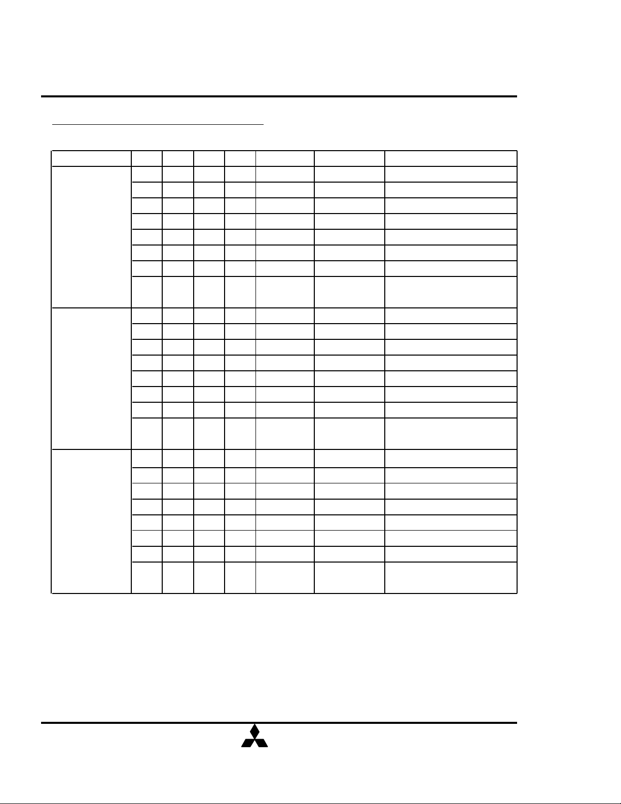
COMMAND TRUTH TABLE
MITSUBISHI LSIs
67108864-BIT (1048576-WORD BY 64-BIT)SynchronousDRAM
COMMAND MNEMONIC
Deselect DESEL H X H X X X X X X
No Operation NOP H X L H H H X X X
Row Adress Entry &
Bank Activate
Single Bank Precharge PRE H X L L H L V L X
Precharge All Bank
Column Address Entry
& Write
Column Address Entry
& Write with Auto-
Precharge
Column Address Entry
& Read
Column Address Entry
& Read with Auto
Precharge
Auto-Refresh REFA H H L HL L H X X X
Self-Refresh Entry REFS H L L L L H X X X
Self-Refresh Exit REFSX L H H
Burst Terminate TERM
Mode Register Set
ACT H X L L H H V V V
PREA
WRITE
WRITEA H X L H L L V H V
READ H X L H L H V L V
READA H X L H L H V H V
MRS
CK
n-1CKn
H X L L H L V H X
H X L LH H L V L V
L H L H H H X X X
H X L H H L X X X
H X L L L L L L
/S
/RAS
LX
/CAS
/WE
X X X X X
BA
A10 A0-9
V*1
H =High Level, L = Low Level, V = Valid, X = Don't Care, n = CK cycle number
NOTE:
1.A7-9 = 0, A0-6 = Mode Address
MIT-DS-0064-0.2
MITSUBISHI
ELECTRIC
( / 45 )
6
Oct.28.1996
Preliminary Spec.
Some contents are subject to change without notice.
MH1S64CWXTJ-12,-15,-1539
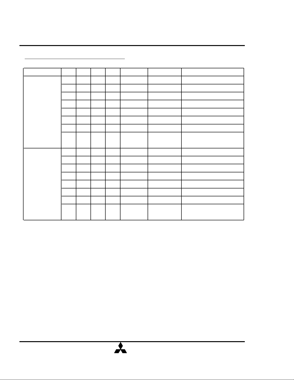
FUNCTION TRUTH TABLE
MITSUBISHI LSIs
67108864-BIT (1048576-WORD BY 64-BIT)SynchronousDRAM
Current State /S /RAS /CAS /WE Address
IDLE H X X X X DESEL NOP
L H H H X NOP NOP
L H H L
L H L X
L L H H
L L H L
L L L H X REFA
L L L L
ROW ACTIVE H X X X X DESEL NOP
L H H H X NOP NOP
L H H L BA TBST NOP
L H L H BA,CA,A10 READ/READA
L H L L BA,CA,A10
L L H H BA,RA ACT Bank Active/ILLEGAL*2
L L H L BA,A10 PRE/PREA Precharge/Precharge All
L L L H X REFA ILLEGAL
L L L L
READ H X X X X DESEL NOP(Continue Burst to END)
L H H H X NOP NOP(Continue Burst to END)
L H H L
L H L H BA,CA,A10 READ/READA
L H L L BA,CA,A10 WRITE/WRITEA
L L H H BA,RA ACT Bank Active/ILLEGAL*2
L L H L BA,A10 PRE/PREA Terminate Burst,Precharge
L L L H X REFA ILLEGAL
L L L L
BA TBST ILLEGAL*2
BA,CA,A10
BA,RA
BA,A10 PRE/PREA NOP*4
Op-Code,
Mode-Add
Op-Code,
Mode-Add
BA
Op-Code,
Mode-Add
Command
READ/WRITE ILLEGAL*2
ACT Bank Active,Latch RA
Auto-Refresh*5
MRS Mode Register Set*5
Begin Read,Latch CA,
Determine Auto-Precharge
WRITE/
WRITEA
MRS ILLEGAL
TBST Terminate Burst
MRS ILLEGAL
Begin Write,Latch CA,
Determine Auto-Precharge
Terminate Burst,Latch CA,
Begin New Read,Determine
Auto-Precharge*3
Terminate Burst,Latch CA,
Begin Write,Determine AutoPrecharge*3
Action
MIT-DS-0064-0.2
MITSUBISHI
ELECTRIC
( / 45 )
7
Oct.28.1996
Preliminary Spec.
Some contents are subject to change without notice.
MH1S64CWXTJ-12,-15,-1539
67108864-BIT (1048576-WORD BY 64-BIT)SynchronousDRAM
FUNCTION TRUTH TABLE(continued)
MITSUBISHI LSIs
Current State /S /RAS /CAS /WE Address
WRITE H X X X X DESEL NOP(Continue Burst to END)
L H H H X NOP NOP(Continue Burst to END)
L H H L BA TBST Terminate Burst
L H L H BA,CA,A10
L H L L BA,CA,A10
L L H H BA,RA ACT Bank Active/ILLEGAL*2
L L H L BA,A10 PRE/PREA Terminate Burst,Precharge
L L L H X REFA ILLEGAL
L L L L
READ with H X X X X DESEL NOP(Continue Burst to END)
AUTO L H H H X NOP NOP(Continue Burst to END)
PRECHARGE L H H L BA TBST ILLEGAL
L H L H BA,CA,A10 READ/READA ILLEGAL
L H L L BA,CA,A10
L L H H BA,RA ACT Bank Active/ILLEGAL*2
L L H L BA,A10 PRE/PREA ILLEGAL*2
L L L H X REFA ILLEGAL
L L L L
WRITE with H X X X X DESEL NOP(Continue Burst to END)
AUTO L H H H X NOP NOP(Continue Burst to END)
PRECHARGE L H H L
L H L H BA,CA,A10 READ/READA ILLEGAL
L H L L BA,CA,A10
L L H H
L L H L BA,A10 PRE/PREA ILLEGAL*2
L L L H X REFA ILLEGAL
L L L L
Op-Code,
Mode-Add
Op-Code,
Mode-Add
BA
BA,RA
Op-Code,
Mode-Add
Command
Terminate Burst,Latch CA,
READ/READA
WRITE/
WRITEA
MRS ILLEGAL
WRITE/
WRITEA
MRS ILLEGAL
TBST ILLEGAL
WRITE/
WRITEA
ACT Bank Active/ILLEGAL*2
MRS ILLEGAL
Begin Read,Determine AutoPrecharge*3
Terminate Burst,Latch CA,
Begin Write,Determine AutoPrecharge*3
ILLEGAL
ILLEGAL
Action
MIT-DS-0064-0.2
MITSUBISHI
ELECTRIC
( / 45 )
8
Oct.28.1996
Preliminary Spec.
Some contents are subject to change without notice.
MH1S64CWXTJ-12,-15,-1539
67108864-BIT (1048576-WORD BY 64-BIT)SynchronousDRAM
FUNCTION TRUTH TABLE(continued)
MITSUBISHI LSIs
Current State /S /RAS /CAS /WE Address
PRE - H X X X X DESEL NOP(Idle after tRP)
CHARGING L H H H X NOP NOP(Idle after tRP)
L H H L BA TBST ILLEGAL*2
L H L X BA,CA,A10 READ/WRITE ILLEGAL*2
L L H H BA,RA ACT ILLEGAL*2
L L H L BA,A10 PRE/PREA NOP*4(Idle after tRP)
L L L H X REFA ILLEGAL
L L L L
ROW H X X X X DESEL NOP(Row Active after tRCD
ACTIVATING L H H H X NOP NOP(Row Active after tRCD
L H H L BA TBST ILLEGAL*2
L H L X BA,CA,A10 READ/WRITE ILLEGAL*2
L L H H BA,RA ACT ILLEGAL*2
L L H L BA,A10 PRE/PREA ILLEGAL*2
L L L H X REFA ILLEGAL
L L L L
Op-Code,
Mode-Add
Op-Code,
Mode-Add
Command
MRS ILLEGAL
MRS ILLEGAL
Action
WRITE RE- H X X X X DESEL NOP
COVERING L H H H X NOP NOP
L H H L BA TBST ILLEGAL*2
L H L X BA,CA,A10 READ/WRITE ILLEGAL*2
L L H H BA,RA ACT ILLEGAL*2
L L H L BA,A10 PRE/PREA ILLEGAL*2
L L L H X REFA ILLEGAL
L L L L
MIT-DS-0064-0.2
Op-Code,
Mode-Add
MITSUBISHI
MRS ILLEGAL
ELECTRIC
( / 45 )
9
Oct.28.1996
Preliminary Spec.
Some contents are subject to change without notice.
MH1S64CWXTJ-12,-15,-1539
67108864-BIT (1048576-WORD BY 64-BIT)SynchronousDRAM
FUNCTION TRUTH TABLE(continued)
Current State /S /RAS /CAS /WE Address Command Action
RE- H X X X X DESEL NOP(Idle after tRC)
FRESHING L H H H X NOP
L H H L BA TBST ILLEGAL
L H L X BA,CA,A10 READ/WRITE ILLEGAL
L L H H BA,RA ACT ILLEGAL
L L H L BA,A10 PRE/PREA ILLEGAL
L L L H X REFA ILLEGAL
L L L L
MODE H X X X X DESEL NOP(Idle after tRSC)
REGISTER L H H H X NOP NOP(Idle after tRSC)
SETTING L H H L BA TBST ILLEGAL
L H L X BA,CA,A10 READ/WRITE ILLEGAL
L L H H BA,RA ACT ILLEGAL
L L H L BA,A10 PRE/PREA ILLEGAL
L L L H X REFA ILLEGAL
L L L L
Op-Code,
MRS ILLEGAL
Mode-Add
Op-Code,
MRS ILLEGAL
Mode-Add
NOP(Idle after tRC)
MITSUBISHI LSIs
ABBREVIATIONS:
H = Hige Level, L = Low Level, X = Don't Care
BA = Bank Address, RA = Row Address, CA = Column Address, NOP = No Operation
NOTES:
1. All entries assume that CKE was High during the preceding clock cycle and the current
clock cycle.
2. ILLEGAL to bank in specified state; function may be legal in the bank indicated by BA,
depending on the state of that bank.
3. Must satisfy bus contention, bus turn around, write recovery requirements.
4. NOP to bank precharging or in idle state.May precharge bank indicated by BA.
5. ILLEGAL if any bank is not idle.
ILLEGAL = Device operation and / or date-integrity are not guaranteed.
MIT-DS-0064-0.2
MITSUBISHI
Oct.28.1996
ELECTRIC
( / 45 )
10
Preliminary Spec.
Some contents are subject to change without notice.
MH1S64CWXTJ-12,-15,-1539
67108864-BIT (1048576-WORD BY 64-BIT)SynchronousDRAM
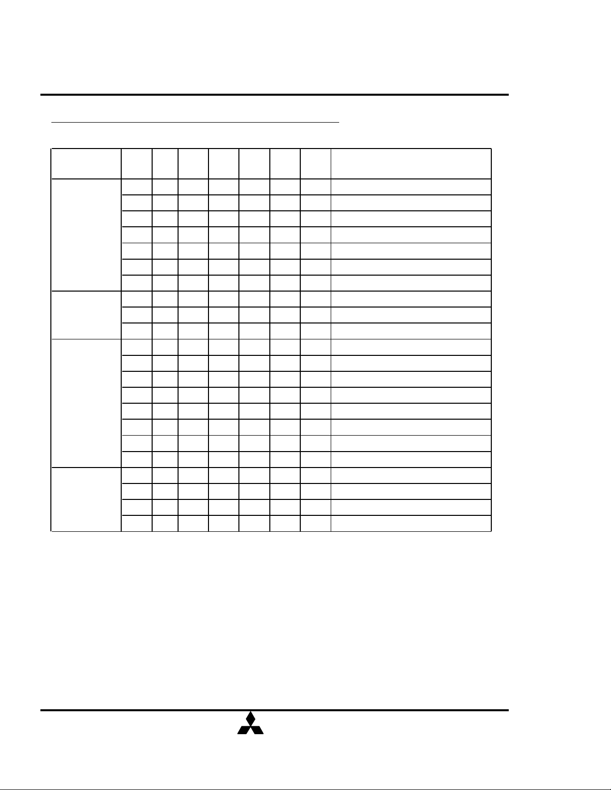
FUNCTION TRUTH TABLE FOR CKE
MITSUBISHI LSIs
Current State
SELF - H X X X X X X
REFRESH*1 L H H X X X X
POWER H X X X X X X
DOWN L H X X X X X
ALL BANKS H H X X X X X
IDLE*2 H L L L L H X
ANY STATE H H X X X X X
other than H L X X X X X
listed above L H X X X X X
CK
n-1CKn
L H L H H H X
L H L H H L X
L H L H L X X
L H L L X X X
L L X X X X X
L L X X X X X
H L H X X X X
H L L H H H X
H L L H H L X
H L L H L X X
H L L L X X X
L X X X X X X
L L X X X X X
/RAS /CAS /WE Add
/S
Action
INVALID
Exit Self-Refresh(Idle after tRC)
Exit Self-Refresh(Idle after tRC)
ILLEGAL
ILLEGAL
ILLEGAL
NOP(Maintain Self-Refresh)
INVALID
Exit Power Down to Idle
NOP(Maintain Self-Refresh)
Refer to Function Truth Table
Enter Self-Refresh
Enter Power Down
Enter Power Down
ILLEGAL
ILLEGAL
ILLEGAL
Refer to Current State = Power Down
Refer to Function Truth Table
Begin CK0 Suspend at Next Cycle*3
Exit CK0 Suspend at Next Cycle*3
Maintain CK0 Suspend
ABBREVIATIONS:
H = High Level, L = Low Level, X = Don't Care
NOTES:
1. CKE Low to High transition will re-enable CK and other inputs asynchronously.
A minimum setup time must be satisfied before any command other than EXIT.
2. Power-Down and Self-Refresh can be entered only form the All banks idle State.
3. Must be legal command.
MIT-DS-0064-0.2
MITSUBISHI
ELECTRIC
( / 45 )
11
Oct.28.1996
Preliminary Spec.
Some contents are subject to change without notice.
MH1S64CWXTJ-12,-15,-1539
67108864-BIT (1048576-WORD BY 64-BIT)SynchronousDRAM
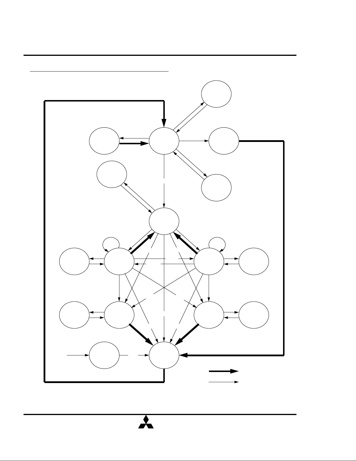
SIMPLIFIED STATE DIAGRAM
MITSUBISHI LSIs
SELF
REFRESH
REFS
REFSX
WRITE
SUSPEND
WRITEA
SUSPEND
MODE
REGISTER
SET
CLK
SUSPEND
CKEL
CKEH
WRITEA READA
CKEL
WRITEA
CKEH
MRS
IDLE
ACT
CKEL
CKEH
ROW
ACTIVE
WRITE READ
READA
READ
READA
PRE
WRITE
WRITEA
WRITE
WRITEA
PRE PRE
REFA
CKEL
CKEH
READ
READA
AUTO
REFRESH
POWER
DOWN
CKEL
CKEH
CKEL
CKEH
READ
SUSPEND
READA
SUSPEND
POWER
APPLIED
MIT-DS-0064-0.2
POWER
ON
PRE
PRE
CHARGE
MITSUBISHI
ELECTRIC
( / 45 )
12
Automatic Sequence
Command Sequence
Oct.28.1996
Preliminary Spec.
Some contents are subject to change without notice.
MITSUBISHI LSIs
MH1S64CWXTJ-12,-15,-1539
67108864-BIT (1048576-WORD BY 64-BIT)SynchronousDRAM
POWER ON SEQUENCE
Before starting normal operation, the following power on sequence is necessary to prevent a
SDRAM from damaged or malfunctioning.
1. Apply power and start clock. Attempt to maintain CKE high, DQMB0-7 high and NOP
condition at the inputs.
2. Maintain stable power, stable cock, and NOP input conditions for a minimum of 500É s.
3. Issue precharge commands for all banks. (PRE or PREA)
4. After all banks become idle state (after tRP), issue 8 or more auto-refresh commands.
5. Issue a mode register set command to initialize the mode register.
After these sequence, the SDRAM is idle state and ready for normal operation.
MODE REGISTER
Burst Length, Burst Type and /CAS Latency can be programmed by setting the mode
register(MRS). The mode register stores these date until the next MRS command, which may
be issue when both banks are in idle state. After tRSC from a MRS command, the SDRAM is
ready for new command.
LATENCY
MODE
BA A10 A9 A8 A7 A6 A5 A4 A3 A2 A1 A0
0 0 0 0 0
CL
0 0 0
0 0 1
0 1 0
0 1 1
1 0 0
1 0 1
1 1 0
1 1 1
/CAS LATENCY
LTMODE BT
R
1
2
3
R
R
R
R
BL
BURST
LENGTH
BURST
TYPE
CK
/S
/RAS
/CAS
/WE
BA, A10 -A0
BL
0 0 0
0 0 1
0 1 0
0 1 1
1 0 0
1 0 1
1 1 0
1 1 1
0
1
V
BT= 0 BT= 1
1
2
4
8
R
R
R
R
SEQUENTIAL
INTERLEAVED
1
2
4
8
R
R
R
R
MIT-DS-0064-0.2
R:Reserved for Future Use
( / 45 )
MITSUBISHI
ELECTRIC
13
Oct.28.1996
Preliminary Spec.
Some contents are subject to change without notice.
MH1S64CWXTJ-12,-15,-1539
CK
Command
Address
DQ
Read
Y
MITSUBISHI LSIs
67108864-BIT (1048576-WORD BY 64-BIT)SynchronousDRAM
Write
Y
Q0 Q1 Q2 Q3
D0 D1
D2
D3
Initial Address
A2 A1 A0
0 0 0
0 0 1
0 1 0
0 1 1
1 0 0
1 0 1
1 1 0
1 1 1
CL= 3
BL= 4
BL
8
/CAS Latency Burst Length Burst Length
Burst Type
Column Addressing
Sequential Interleaved
0 1 2 3 4 5 6 7 0 1 2 3 4 5 6 7
1 2 3 4 5 6 7 0 1 0 3 2 5 4 7 6
2 3 4 5 6 7 0 1 2 3 0 1 6 7 4 5
3 4 5 6 7 0 1 2 3 2 1 0 7 6 5 4
4 5 6 7 0 1 2 3 4 5 6 7 0 1 2 3
5 6 7 0 1 2 3 4 5 4 7 6 1 0 3 2
6 7 0 1 2 3 4 5 6 7 4 5 2 3 0 1
7 0 1 2
3 4 5 6 3 2 1 0
7 6 5 4
- 0 0
- 0 1
- 1 0
- 1 1
- - 0
- - 1
MIT-DS-0064-0.2
0 1 2 3
1 2 3 0
4
2 3 0 1
3 0
0 1
2
1 0
1 2
MITSUBISHI
ELECTRIC
( / 45 )
14
0 1 2 3
1 0 3 2
2 3 0 1
3 2
0 1
1 0
1 0
Oct.28.1996

Preliminary Spec.
Some contents are subject to change without notice.
MITSUBISHI LSIs
MH1S64CWXTJ-12,-15,-1539
67108864-BIT (1048576-WORD BY 64-BIT)SynchronousDRAM
OPERATION DESCRIPTION
BANK ACTIVATE
The SDRAM has two independent banks. Each bank is activated by the ACT command with
the bank address(BA). A row is indicated by the row address A10-0. The minimum activation
interval between one bank and the other bank is tRRD.
PRECHARGE
The PRE command deactivates indicated by BA. When both banks are active, the precharge
all command(PREA,PRE + A10=H) is available to deactivate them at the same time. After tRP
from the precharge, an ACT command can be issued.
Bank Activation and Precharge All (BL=4, CL=3)
CK
Command
A0-9
A10
BA
DQ
ACT
Xa
Xa
0
tRRD
tRCD
ACT
Xb
Xb
1
READ
Y
0
0
PRE
tRAS tRP
1
Qa0 Qa1 Qa2 Qa3
Precharge all
ACT
Xb
Xb
1
READ
After tRCD from the bank activation, a READ command can be issued. 1st output date is
available after the /CAS Latency from the READ, followed by (BL-1) consecutive date when
the Burst Length is BL. The start address is specified by A7-0, and the address sequence of
burst data is defined by the Burst Type. A READ command may be applied to any active bank,
so the row precharge time(tRP) can be hidden behind continuous output data(in case of BL=8)
by interleaving the dual banks. When A10 is high at a READ command, the
auto-precharge(READA) is performed. Any command (READ, WRITE, PRE, ACT) to the
same bank is inhibited till the internal precharge is complete. The internal precharge start
timing depends on /CAD Latency. The next ACT command can be issued after tRP from the
internal precharge timing.
MIT-DS-0064-0.2
MITSUBISHI
ELECTRIC
( / 45 )
15
Oct.28.1996

Preliminary Spec.
Some contents are subject to change without notice.
MH1S64CWXTJ-12,-15,-1539
Dual Bank Interleaving READ (BL=4, CL=3)
CK
MITSUBISHI LSIs
67108864-BIT (1048576-WORD BY 64-BIT)SynchronousDRAM
Command
A0-9
A10
BA
DQ
CK
Command
A0-9
A10
BA
ACT
tRCD
Xa
Xa
0
READ
Y
0
0
ACT
Xb
Xb
1
/CAS latency
READ
Qa0 Qa1 Qa2 Qa3 Qb0 Qb1 Qb2
Burst Length
READ with Auto-Precharge (BL=4, CL=3)
ACT
tRCD tRP
Xa
Xa
0
READ
Y
1
0
PRE
Y
0
0
1
0
ACT
Xa
Xa
0
DQ
CK
Command
CL=3
CL=2
MIT-DS-0064-0.2
Qa0 Qa1 Qa2 Qa3
Internal precharge begins
READ Auto-Precharge Timing (BL=4)
ACT READ
DQ Qa0 Qa1 Qa2 Qa3
DQ Qa0 Qa1 Qa2 Qa3
DQ Qa0 Qa1 Qa2 Qa3CL=1
Internal Precharge Start Timing
MITSUBISHI
ELECTRIC
( / 45 )
16
Oct.28.1996

Preliminary Spec.
Some contents are subject to change without notice.
MITSUBISHI LSIs
MH1S64CWXTJ-12,-15,-1539
67108864-BIT (1048576-WORD BY 64-BIT)SynchronousDRAM
WRITE
After tRCD from the bank activation, a WRITE command can be issued. 1st input data is set
at the same cycle as the WRITE. Following(BL-1) data are written into the RAM, when the
Burst Length is BL. The start address is specified by A7-0, and the address sequence of burst
data is defined by the Burst Type. A WRITE command may be applied to any active bank, so
the row precharge time(tRP) can be hidden behind continuous input data (in case of BL=4) by
interleaving the dual banks. From the last input data to the PRE command, the write recovery
time (tWR) is required. When A10 is high at a WRITE command, the auto-precharge(WRITEA)
is performed. Any command(READ, WRITE, PRE, ACT) to the same bank is inhibited till the
internal precharge is complete. The internal precharge begins at tWR after the last input data
cycle. The next ACT command can be issued after tRP from the internal precharge timing.
Dual Bank Interleaving WRITE (BL=4)
CK
Command
A0-9
A10
BA
DQ
CK
Command
A0-9
A10
ACT
tRCD
Xa
Xa
0
Write
ACT
tRCD
Y
Xb
0
Xb
0
1
Da0 Da1 Da2 Da3
Burst Length
WRITE with Auto-Precharge (BL=4)
ACT
tRCD tRP
Xa
Xa
Write
Y
1
Write
PRE
Y
tWR
0
0
1
0
Db0 Db1 Db2 Db3
ACT
Xa
Xa
BA
DQ
MIT-DS-0064-0.2
0
0
Da0 Da1 Da2 Da3
MITSUBISHI
0
tWR
Internal precharge begins
Oct.28.1996
ELECTRIC
17
( / 45 )

Preliminary Spec.
Some contents are subject to change without notice.
MITSUBISHI LSIs
MH1S64CWXTJ-12,-15,-1539
67108864-BIT (1048576-WORD BY 64-BIT)SynchronousDRAM
BURST INTERRUPTION
[ Read Interrupted by Read ]
Burst read option can be interrupted by new read of the same or the other bank. MH4S64CTJ
allows random column access. READ to READ interval is minimum 1 CK
Read Interrupted by Read (BL=4, CL=3)
CK
Command
A0-9
A10
BA
DQ
READ
Yi
0
0
READ
Yj
0
0
READ
Yk
0
1
Qai0 Qaj1 Qbk0 Qbk1
Qaj0 Qbk2 Qal0
READ
Yl
0
0
Qal1 Qal2 Qal3
[ Read Interrupted by Write ]
Burst read operation can be interrupted by write of the same or the other bank. Random
column access is allowed. In this case, the DQ should be controlled adequately by using the
DQMB0-7 to prevent the bus contention. The output is disabled automatically 2 cycle after
WRITE assertion.
Read Interrupted by Write (BL=4, CL=3)
CK
Command
READ
Write
A0-9
A10
BA
DQMB0-7
Q
D
MIT-DS-0064-0.2
Yi
0
0
Qai0
Yj
0
0
Daj0 Daj1 Daj2 Daj3
DQM control Write control
MITSUBISHI
Oct.28.1996
ELECTRIC
18
( / 45 )

Preliminary Spec.
Some contents are subject to change without notice.
MITSUBISHI LSIs
MH1S64CWXTJ-12,-15,-1539
67108864-BIT (1048576-WORD BY 64-BIT)SynchronousDRAM
[ Read Interrupted by Precharge ]
Burst read operation can be interrupted by precharge of the same or the other bank. Read
to PRE interval is minimum 1 CK. A PRE command disables the data output, depending on
the /CAS Latency. The figure below shows examples, when the dataout is terminated.
Read Interrupted by Precharge (BL=4)
CK
CL=4
CL=3
CL=2
Command
DQ
Command
DQ
Command
DQ
Command
DQ
Command
DQ
READ PRE
Q0 Q2 Q3Q1
READ
READ PRE
READ PRE
READ
PRE
Q0 Q1
Q0 Q1
Q0 Q1
PRE
Q0 Q2 Q3Q1
Q2 Q3
CL=
1
MIT-DS-0064-0.2
Command
DQ
Comman
d
DQ
Comman
d
DQ
READ PRE
Q0 Q1
REA
D
Q
Q
0
1
REA
D
PR
E
Q
Q
0
1
MITSUBISHI
ELECTRIC
19
( / 45 )
PRE
Q2Q
3
Oct.28.1996

Preliminary Spec.
Some contents are subject to change without notice.
MITSUBISHI LSIs
MH1S64CWXTJ-12,-15,-1539
67108864-BIT (1048576-WORD BY 64-BIT)SynchronousDRAM
[ Read Interrupted by Burst Terminate ]
Similarly to the precharge, burst terminate command can interrupt burst read operation and
disable the data output. READ to TERM interval is minimum 1 CK. The figure below shows
examples, when the dataout is terminated.
Read Interrupted by Burst Terminate (BL=4)
CK
CL=3
CL=2
Command
DQ
Command
DQ
Command
DQ
Command
DQ
Command
DQ
READ TERM
Q0 Q1
READ TERM
Q0 Q1 Q2
READ TERM
Q0
READ
Q0 Q1 Q2 Q3
READ
Q0 Q1 Q2
TERM
TERM
Q2 Q3
CL=1
MIT-DS-0064-0.2
Command
DQ
Command
DQ
Command
DQ
READ
TERM
READ
Q0 Q1 Q2 Q3
READ TERM
Q0
MITSUBISHI
ELECTRIC
20
( / 45 )
Q0
TERM
Oct.28.1996

Preliminary Spec.
Some contents are subject to change without notice.
MITSUBISHI LSIs
MH1S64CWXTJ-12,-15,-1539
67108864-BIT (1048576-WORD BY 64-BIT)SynchronousDRAM
[ Write Interrupted by Write ]
Burst write operation can be interrupted by new write of the same or the other bank.
Random column access is allowed. WRITE to WRITE interval is minimum 1 CK.
Write Interrupted by Write (BL=4)
CK
Command
A0-9
A10
BA
DQ
Write
Write
Yi
Yj
0
0
0
0
Dai0 Daj0 Daj1 Dbk0
Write
Yk
0
1
Dbk1 Dbk2
Write
Yl
0
0
Dal0 Dal1 Dal2 Dal3
[ Write Interrupted by Read ]
Burst write operation can be interrupted by read of the same or the other bank.
Random column access is allowed. WRITE to READ interval is minimum 1 CK. The
input data on DQ at the interrupting READ cycle is "don't care".
Write Interrupted by Read (BL=4, CL=3)
CK
Command
Write
READ
Write
READ
A0-9
A10
BA
DQMB0-7
DQ
MIT-DS-0064-0.2
Yi
Yj
0
0
0
0
Qaj0
Qaj1Dai0 Dak0 Dak1
MITSUBISHI
Yk
0
0
Yl
0
1
Qbl0
Oct.28.1996
ELECTRIC
21
( / 45 )

Preliminary Spec.
Some contents are subject to change without notice.
MH1S64CWXTJ-12,-15,-1539
[ Write Interrupted by Precharge ]
Burst write operation can be interrupted by precharge of the same bank. Random
column access is allowed. Because the write recovery time(tWR) is required between
the last input data and the next PRE, 3rd data should be masked with DQMB0-7
shown as below.
Write Interrupted by Precharge (BL=4)
CK
MITSUBISHI LSIs
67108864-BIT (1048576-WORD BY 64-BIT)SynchronousDRAM
Command
A0-9
A10
BA
DQMB0-7
DQ
Write
Yi
0
0
Dai0 Dai1
PRE
tWR tRP
0
0
This data should be masked to satisfy tWR requirement.
ACT
Xb
Xb
0
[ Write Interrupted by Burst Terminate ]
Burst terminate command can terminate burst write operation. In this case, the write
recovery time is not required and the bank remains active. The figure below shows
the case 3 words of data are written. Random column access is allowed. WRITE to
TERM interval is minimum 1 CK.
Write Interrupted by Burst Terminate (BL=4)
Command
DQMB0-7
MIT-DS-0064-0.2
CK
A0-9
A10
BA
DQ
Write
Yi
0
0
Dai0 Dai1
Dai2
TERM
( / 45 )
MITSUBISHI
ELECTRIC
22
Oct.28.1996

Preliminary Spec.
Some contents are subject to change without notice.
MH1S64CWXTJ-12,-15,-1539
AUTO REFRESH
Single cycle of auto-refresh is initiated with a REFA(/CS=/RAS=/CAS=L,
/WE=/CKE=H) command. The refresh address is generated internally. 4096 REFA
cycle within 64ms refresh 16Mbit memory cells. The auto-refresh is performed on
each bank alternately(ping-pong refresh). Before performing an auto-refresh, both
banks must be in the idle state. Additional commands must not be supplied to the
device before tRC from the REFA command.
Auto-Refresh
CK
/S
/RAS
MITSUBISHI LSIs
67108864-BIT (1048576-WORD BY 64-BIT)SynchronousDRAM
NOP or DESLECT
/CAS
/WE
CKE
A0-10
BA
minimum tRC
Auto Refresh on Bank 0 Auto Refresh on Bank 1
MIT-DS-0064-0.2
MITSUBISHI
ELECTRIC
23
( / 45 )
Oct.28.1996

Preliminary Spec.
Some contents are subject to change without notice.
MH1S64CWXTJ-12,-15,-1539
SELF REFRESH
Self-refresh mode is entered by issuing a REFS command (/CS=/RAS=/CAS=L,
/WE=H, CKE=L). Once the self-refresh is initiated, it is maintained as log as CKE is
kept low.During the self-refresh mode, CKE is asynchronous and the only enabled
input (but asynchronous), all other inputs including CK0 are disabled and ignored, and
power consumption due to synchronous inputs is saved. To exit the self-refresh,
supplying stable CK0 inputs, asserting DESEL or NOP command and then asserting
CKE(REFSX). After tRC from REFSX both banks are in the idle state and a new
command can be issued after tRC, but DESEL or NOP commands must be asserted
till then.
Self-Refresh
CK
/S
MITSUBISHI LSIs
67108864-BIT (1048576-WORD BY 64-BIT)SynchronousDRAM
Stable CK
NOP
/RAS
/CAS
/WE
CKE
A0-10
BA
Self Refresh Entry Self Refresh Exit
new command
X
0
minimum tRC
for recovery
MIT-DS-0064-0.2
MITSUBISHI
ELECTRIC
24
( / 45 )
Oct.28.1996

Preliminary Spec.
Some contents are subject to change without notice.
MH1S64CWXTJ-12,-15,-1539
CLK SUSPEND
CKE controls the internal CLK at the following cycle. Figure below shows how CKE
works. By negating CKE, the next internal CLK is suspended. The purpose of CLK
suspend is power down, output suspend or input suspend. CKE is a synchronous
input except during the self-refresh mode. CLK suspend can be performed either
when the banks are active or idle, but a command at the following cycle is ignored.
CK
(ext.CLK)
CKE
int.CLK
MITSUBISHI LSIs
67108864-BIT (1048576-WORD BY 64-BIT)SynchronousDRAM
CK
CKE
Command
CKE
Command
CK
CKE
PRE
ACT
Power Down by CKE
Standby Power Down
NOP NOP NOP NOP NOP NOP
NOP
Active Power Down
NOP NOP NOP NOP NOP NOP
NOP
DQ Suspend by CKE
Command
MIT-DS-0064-0.2
DQ
Write
D0 D1 D2 D3
25
( / 45 )
READ
MITSUBISHI
ELECTRIC
Q0 Q1 Q2 Q3
Oct.28.1996

Preliminary Spec.
Some contents are subject to change without notice.
MH1S64CWXTJ-12,-15,-1539
DQM CONTROL
DQMB0-7 is a dual function signal defined as the data mask for writes and the output
disable for reads. During writes, DQMB0-7 masks input data word by word. DQMB0-7
to write mask latency is 0.
During reads, DQMB0-7 forces output to Hi-Z word by word. DQMB0-7 to output Hi-Z
latency is 2.
CK
MITSUBISHI LSIs
67108864-BIT (1048576-WORD BY 64-BIT)SynchronousDRAM
DQM Function
Command
DQMB0-7
DQ
Write
D0 D2 D3
masked by DQM=H
READ
Q0 Q1 Q3
disabled by DQM=H
MIT-DS-0064-0.2
MITSUBISHI
ELECTRIC
26
( / 45 )
Oct.28.1996

Preliminary Spec.
Some contents are subject to change without notice.
MH1S64CWXTJ-12,-15,-1539
ABSOLUTE MAXIMUM RATINGS
MITSUBISHI LSIs
67108864-BIT (1048576-WORD BY 64-BIT)SynchronousDRAM
Symbol Parameter
Vdd
VI
VO
IO
Pd
Topr
Tstg
Supply Voltage
Input Voltage
Output Voltage
Output Current
Power Dissipation
Operating Temperature
Storage Temperature
Condition Ratings Unit
with respect to Vss
with respect to Vss
with respect to Vss
Ta=25°C
RECOMMENDED OPERATING CONDITION
(Ta=0 ~ 70°C, unless otherwise noted)
Symbol
Vdd
Vss
Parameter
Supply Voltage
Supply Voltage
-0.5 ~ 4.6
-0.5 ~ 4.6
-0.5 ~ 4.6
50
4
0 ~ 70
-40 ~ 100
Limits
Min. Typ. Max.
3.0
0
3.3
0
3.6
0
V
V
V
mA
W
°C
°C
Unit
V
V
VIH
VIL
High-Level Input Voltage all inputs
Low-Level Input Voltage all inputs
2.0
-0.3
CAPACITANCE
(Ta=0 ~ 70°C, Vdd = 3.3 ± 0.3V, Vss = 0V, unless otherwise noted)
Symbol
CI(A)
CI(C)
CI(K)
CI/O
MIT-DS-0064-0.2
Parameter
Input Capacitance, address pin
Input Capacitance, control pin
Input Capacitance, CK pin
Input Capacitance, I/O pin
( / 45 )
Test Condition Limits(max.) Unit
VI = Vss
f=1MHz
Vi=25mVrms
MITSUBISHI
ELECTRIC
27
Vdd+0.3
30
30
15
12
0.8
V
V
pF
pF
pF
pF
Oct.28.1996

Preliminary Spec.
Some contents are subject to change without notice.
MH1S64CWXTJ-12,-15,-1539
67108864-BIT (1048576-WORD BY 64-BIT)SynchronousDRAM
AVERAGE SUPPLY CURRENT from Vdd
(Ta=0 ~70°C, Vdd = 3.3 ± 0.3V, Vss = 0V, unless otherwise noted)
MITSUBISHI LSIs
Symbol Parameter
Icc1s
Icc1d
Icc2h standby current, CKE=H
Icc2l standby current, CKE=L
Icc3 active standby current mA
Icc4
Icc5 auto-refresh current tRC=min, tCLK=min mA
Icc6 self-refresh current CKE <0.2V mA
operating current, single bank
operating current, dual bank
burst current
tRC=min.tCLK=min, BL=1, CL=3 mA
tRC=min.tCLK=min, BL=1, CL=3
both banks idle, tCLK=min, CKE=H
both banks idle, tCLK=min, CKE=L
both banks active, tCLK=min, CKE=H
tCLK=min, BL=4, CL=3, 1 bank idle(discerte)
Test Condition
Limits(max)
-12 -15 -1539
360 300
360
520 440
520
72 64
72
8 8
8
140 120
140
480 400
480
240 200
240
4
4
4
AC OPERATING CONDITIONS AND CHARACTERISTICS
(Ta=0 ~ 70°C, Vdd = 3.3 ± 0.3V, Vss = 0V, unless otherwise noted)
Symbol Parameter Test Condition
VOH(DC) High-Level Output Voltage(DC) IOH=-2mA 2.4 V
VOL(DC)
VOH(AC)High-Level Output Voltage(AC) CL=50pF,
IOZ Off-stare Output Current Q floating VO=0 ~ Vdd -10 10 uA
VOL(AC) Low-Level Output Voltage(AC) CL=50pF, IOL=2mA 0.8 V
Low-Level Output Voltage(DC)
Input Current
Ii
IOL=2mA 0.4 V
IOH=-2mA
VIH=0 ~ Vdd+0.3V
Limits
Min. Max.
2 V
-40
40 uA
Unit
Unit
mA
mA
mA
mA
MIT-DS-0064-0.2
MITSUBISHI
ELECTRIC
28
( / 45 )
Oct.28.1996

Preliminary Spec.
Some contents are subject to change without notice.
MITSUBISHI LSIs
MH1S64CWXTJ-12,-15,-1539
67108864-BIT (1048576-WORD BY 64-BIT)SynchronousDRAM
AC TIMING REQUIREMENTS
(Ta=0 ~ 70°C, Vdd = 3.3 ± 0.3V, Vss = 0V, unless otherwise noted)
Input Pulse Levels: 0.8V to 2.0V
Input Timing Measurement Level: 1.4V
Limits
Symbol Parameter -15 -1539 Unit
CL=1
tCLK CK cycle time
tCH CK High pulse width 4
tCL CK Low pilse width 4 4 ns
tT Transition time of CK 1 10 1 10 ns
tIS Input Setup time(all inputs) 3 3 ns
tIH Input Hold time(all inputs) 1 1.5 ns
tRC Row cycle time 100 120 ns
tRCD Row to Column Delay 30 30 ns
tRAS Row Active time 70 10000 80 10000 ns
tRP Row Precharge time 30 40 ns
tWR Write Recovery time 12 15 ns
tRRD Act to Act Deley time 24 30 ns
tRSC Mode Register Set Cycle time 24 30 ns
tPDE Power Down Exit time 12 15 ns
tREF Refresh Interval time 65.6 65.6 ms
CL=2
CL=3
-12
Min.
Max.
30
15
12
4
4
1 10
3
1
100
30
70 10000
30
12
24
24
12
65.6
Min. Max. Min. Max.
30 30
15 20
12
15
4 ns
ns
ns
ns
CK
Signal
MIT-DS-0064-0.2
MITSUBISHI
ELECTRIC
29
( / 45 )
1.4V
1.4V
Any AC timing is
referenced to the input
signal crossing through
1.4V.
Oct.28.1996

Preliminary Spec.
Some contents are subject to change without notice.
MH1S64CWXTJ-12,-15,-1539
67108864-BIT (1048576-WORD BY 64-BIT)SynchronousDRAM
SWITCHING CHARACTERISTICS
(Ta=0 ~ 70°C, Vdd = 3.3 ± 0.3V, Vss = 0V, unless otherwise noted)
Limits
Symbol Parameter -12
Min. Max. Min. Max. Min. Max.
CL=1 27 27 30 ns
tAC Access time from CK CL=2
CL=3 8
tCAC Column Access Time
tRAC Row Access Time
tOH
tOLZ
tOHZ
Output Hold time
from CK
Delay time, output low
impedance from CK
Delay time, output high
impedance from CK
3 3 3 ns
0 0 0 ns
3 8 3 8 3 10 ns
9.5
24.5
54.5
-15 -1539
MITSUBISHI LSIs
Uni
t
9.5 12 ns
8 9
ns
24.5 30 ns
54.5 60 ns
Output Load
Condition
VOUT
50Ω
50pF
CK
VTT=1.4V
tAC tOH
CK
Output Timing
Measurement
Reference Point
tOHZ
DQ
1.4V
1.4V
1.4V
1.4VDQ
MIT-DS-0064-0.2
MITSUBISHI
ELECTRIC
30
( / 45 )
Oct.28.1996

Preliminary Spec.
Some contents are subject to change without notice.
MH1S64CWXTJ-12,-15,-1539
WRITE CYCLE (single bank) BL=4
CK
/S
MITSUBISHI LSIs
67108864-BIT (1048576-WORD BY 64-BIT)SynchronousDRAM
tRC
/RAS
/CAS
/WE
CKE
DQMB
0-7
A0-9
A10
tRAS
tRCD
X
X
Y
tRP
X
X
BA
DQ
MIT-DS-0064-0.2
D D D D
MITSUBISHI
ELECTRIC
31
( / 45 )
tWR
Oct.28.1996
Preliminary Spec.
Some contents are subject to change without notice.
MH1S64CWXTJ-12,-15,-1539
MITSUBISHI LSIs
67108864-BIT (1048576-WORD BY 64-BIT)SynchronousDRAM
CK
/S
/RAS
/CAS
/WE
CKE
DQMB
0-7
WRITE CYCLE (dual bank)
tRC
tRAS
tRRD
tRCD
tRCD
BL=4
tRP
tRAS
A0-9
A10
BA
DQ
MIT-DS-0064-0.2
Xa
Xa
Y
Da
Xb
Xb
Da
Da Da
MITSUBISHI
ELECTRIC
32
( / 45 )
Y
tWR
Db Db Db Db
tWR
Oct.28.1996

Preliminary Spec.
Some contents are subject to change without notice.
MH1S64CWXTJ-12,-15,-1539
MITSUBISHI LSIs
67108864-BIT (1048576-WORD BY 64-BIT)SynchronousDRAM
CK
/S
/RAS
/CAS
/WE
CKE
DQMB
0-7
READ CYCLE (single bank)
tRC
tRAS
tRCD
BL=4, CL=3
tRP
A0-9
A10
BA
DQ
MIT-DS-0064-0.2
X
X
Y
tRAC
tCAC
Q Q
MITSUBISHI
X
X
QQ
Oct.28.1996
ELECTRIC
33
( / 45 )

Preliminary Spec.
Some contents are subject to change without notice.
MH1S64CWXTJ-12,-15,-1539
CK
/S
tRAS
tRRD
/RAS
MITSUBISHI LSIs
67108864-BIT (1048576-WORD BY 64-BIT)SynchronousDRAM
BL=4, CL=3READ CYCLE (dual bank)
tRC
tRP
tRAS
/CAS
/WE
CKE
DQMB
0-7
A0-9
A10
BA
Xa
Xa
tRCD
tRCD
Y
Xb
Xb
Y
Xa
Xa
DQ
MIT-DS-0064-0.2
tRAC
tCAC
tRAC
MITSUBISHI
ELECTRIC
34
( / 45 )
Qa Qa
tCAC
QaQa
Qb Qb QbQb
Oct.28.1996

Preliminary Spec.
Some contents are subject to change without notice.
MH1S64CWXTJ-12,-15,-1539
MITSUBISHI LSIs
67108864-BIT (1048576-WORD BY 64-BIT)SynchronousDRAM
CK
/S
/RAS
/CAS
/WE
CKE
DQMB
0-7
WRITE to READ (single bank)
tRAS
tRCD
BL=4, CL=3
A0-9
A10
BA
DQ
MIT-DS-0064-0.2
X
X
Y
D D D D
MITSUBISHI
Y
Q Q Q Q
tCAC
Oct.28.1996
ELECTRIC
35
( / 45 )

Preliminary Spec.
Some contents are subject to change without notice.
MH1S64CWXTJ-12,-15,-1539
MITSUBISHI LSIs
67108864-BIT (1048576-WORD BY 64-BIT)SynchronousDRAM
CK
/S
/RAS
/CAS
/WE
CKE
DQMB
0-7
WRITE to READ (dual bank)
tRC
tRAS
tRRD
tRCD
tRCD
BL=4, CL=3
tRP
tRAS
A0-9
A10
BA
DQ
MIT-DS-0064-0.2
Xa
Xa
Y
Da
Xb
Xb
Da
Da Da
MITSUBISHI
ELECTRIC
36
( / 45 )
Y
tWR
tCAC
Qb Qb
Xa
Xa
Qb
Oct.28.1996
Qb

Preliminary Spec.
Some contents are subject to change without notice.
MH1S64CWXTJ-12,-15,-1539
MITSUBISHI LSIs
67108864-BIT (1048576-WORD BY 64-BIT)SynchronousDRAM
CK
/S
/RAS
/CAS
/WE
CKE
DQMB
0-7
READ to WRITE (single bank)
tRAS
tRCD
for output diable
BL=4, CL=3
A0-9
A10
BA
DQ
MIT-DS-0064-0.2
X
X
Y
tRAC
tCAC
Q Q
MITSUBISHI
Y
tWR
D D D D
Oct.28.1996
ELECTRIC
37
( / 45 )

Preliminary Spec.
Some contents are subject to change without notice.
MH1S64CWXTJ-12,-15,-1539
MITSUBISHI LSIs
67108864-BIT (1048576-WORD BY 64-BIT)SynchronousDRAM
CK
/S
/RAS
/CAS
/WE
CKE
DQMB
0-7
READ to WRITE (dual bank)
tRC
tRAS
tRRD
tRCD
for output disable
BL=4, CL=3
tRP
tRAS
tRCD
A0-9
A1
0
BA
DQ
MIT-DS-0064-0.2
Xa
Xa
Y
tRAC
Xb
Xb
tCAC
Qa
MITSUBISHI
ELECTRIC
38
( / 45 )
Qa
Y
Db Db Db Db
Xa
Xa
tWR
Oct.28.1996

Preliminary Spec.
Some contents are subject to change without notice.
MH1S64CWXTJ-12,-15,-1539
WRITE with AUTO-PRECHARGE BL=4
CK
/S
/RAS
tRCD
/CAS
MITSUBISHI LSIs
67108864-BIT (1048576-WORD BY 64-BIT)SynchronousDRAM
tRC
tWR + tRP
/WE
CKE
DQMB
0-7
A0-9
A10
BA
DQ
X
X
Y
D D D D
X
X
internal precharge starts
this timing depends on
BL
MIT-DS-0064-0.2
MITSUBISHI
ELECTRIC
39
( / 45 )
Oct.28.1996

Preliminary Spec.
Some contents are subject to change without notice.
MH1S64CWXTJ-12,-15,-1539
READ with AUTO-PRECHARGE BL=4, CL=3
CK
/S
/RAS
tRCD
/CAS
MITSUBISHI LSIs
67108864-BIT (1048576-WORD BY 64-BIT)SynchronousDRAM
tRC
tRP
/WE
CKE
DQMB
0-7
A0-9
A10
BA
DQ
X
X
Y
tRAC
tCAC
Q Q
internal precharge starts @CL=3, BL=4
this timing depends on CL and BL
Q
Q
X
X
MIT-DS-0064-0.2
MITSUBISHI
ELECTRIC
40
( / 45 )
Oct.28.1996

Preliminary Spec.
Some contents are subject to change without notice.
MH1S64CWXTJ-12,-15,-1539
AUTO-REFRESH
CK
/S
tRP
/RAS
/CAS
MITSUBISHI LSIs
67108864-BIT (1048576-WORD BY 64-BIT)SynchronousDRAM
tRC
/WE
CKE
DQMB
0-7
A0-9
A10
BA
DQ
if any bank is active, it must be precharged
MIT-DS-0064-0.2
MITSUBISHI
ELECTRIC
41
( / 45 )
Oct.28.1996

Preliminary Spec.
Some contents are subject to change without notice.
MH1S64CWXTJ-12,-15,-1539
SELF-REFRESH ENTRY
CK
/S
tRP
/RAS
/CAS
MITSUBISHI LSIs
67108864-BIT (1048576-WORD BY 64-BIT)SynchronousDRAM
/WE
CKE
DQMB
0-7
A0-9
A10
BA
DQ
if any bank is active, it must be precharged
MIT-DS-0064-0.2
MITSUBISHI
ELECTRIC
42
( / 45 )
Oct.28.1996

Preliminary Spec.
Some contents are subject to change without notice.
MH1S64CWXTJ-12,-15,-1539
SELF-REFRESH EXIT
CK
/S
/RAS
/CAS
MITSUBISHI LSIs
67108864-BIT (1048576-WORD BY 64-BIT)SynchronousDRAM
NOP or DESEL
/WE
CKE
DQMB
0-7
A0-9
A10
BA
DQ
tRC
X
X
internal CLK re-start
MIT-DS-0064-0.2
MITSUBISHI
ELECTRIC
43
( / 45 )
Oct.28.1996
Preliminary Spec.
Some contents are subject to change without notice.
MH1S64CWXTJ-12,-15,-1539
MODE REGISTER SET BL=4, CL=3
CK
/S
MITSUBISHI LSIs
67108864-BIT (1048576-WORD BY 64-BIT)SynchronousDRAM
/RAS
/CAS
/WE
CKE
DQMB
0-7
A0-9
A10
tRP
mode
tRSC
tRCD
X
X
Y
BA
DQ
MIT-DS-0064-0.2
if any bank is active, it must be precharged
MITSUBISHI
ELECTRIC
44
( / 45 )
Q Q Q
tCAC
tRAC
Oct.28.1996

Preliminary Spec.
Some contents are subject to change without notice.
MH1S64CWXTJ-12,-15,-1539
Outline
MITSUBISHI LSIs
67108864-BIT (1048576-WORD BY 64-BIT)SynchronousDRAM
3.9MAX
133.35±0.13
127.35±0.13
1±0.13
2-R2±0.13
1.27±0.1
17.78±0.13
2-ø3±0.1
841
1.27±0.1
43x1.27=54.61±0.2
MIT-DS-0064-0.2
3±0.13
1±0.13
2±0.13
3±0.13
17.78±0.13
25.4±0.13
MITSUBISHI
ELECTRIC
( / 45 )
45
42.18±0.13
29x1.27=36.83±0.2
9x1.27=11.43±0.2 6.35±0.1
6.35±0.13
24.495±0.13
8.89±0.13
Oct.28.1996
 Loading...