

Page 1
MITSUBISHI SEMICONDUCTOR
MGFS36E2527
Specifications are subject to change without notice. 2.5-2.7GHz HBT HYBRID IC
DESCRIPTION
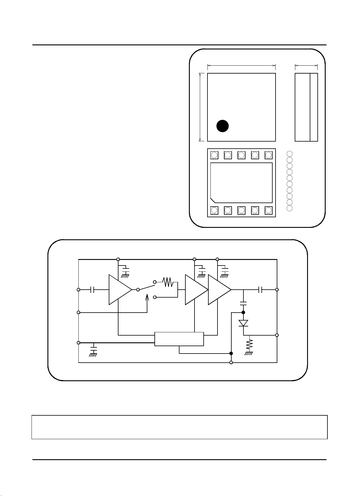
Outline Drawing
4.5 1.0
MGFS36E2527 is a GaAs RF amplifier designed
for WiMAX CPE.
FEATURES
• InGaP HBT Device
• 6V Operation
• 27dBm Linear Output Power
4.5
36E
2527
(Lot No.)
• 33dB Linear Gain
• Integrated Output Power Detector
• Integrated 1-bit 19dB Step Attenuator
• 50ohms Matched
• Surface Mount Package
• RoHS Compliant Package
APPLICATIONS
IEEE802.16-2004, IEEE802.16e-2005
10 89
1 2 3
67
54
(X-ray Top View)
1
2
3
4
5
6
7
8
9
10
Pin
Vc (Vcb)
Vc (Vc1)
Vc (Vc2)
Vc (Vc3)
Pout
Po_det
GND
Vref
Vcont
DIM IN mm
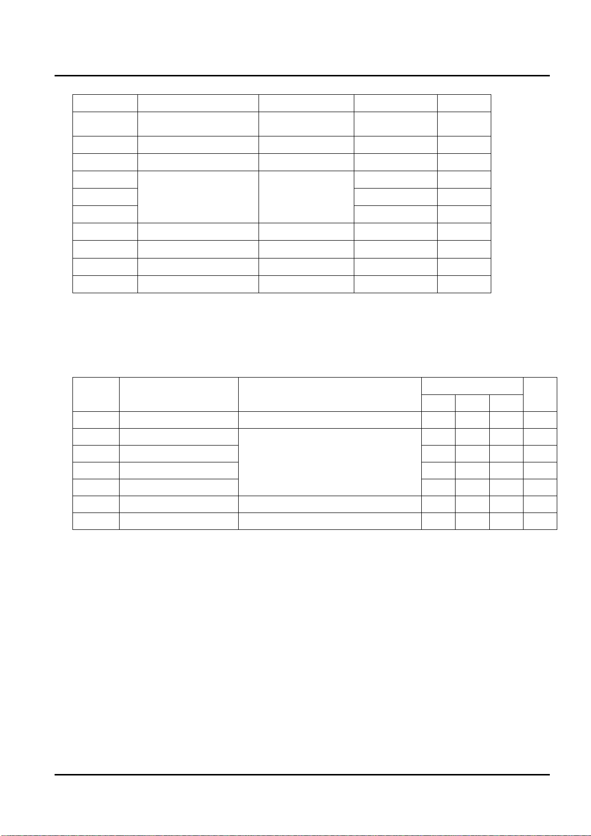
FUNCTIONAL BLOCK DIAGRAM
Pin
Vc1
Vc2
1000pF
Vc3
1000pF
1000pF
Pout
Vcont
(0/3V)
Po_det
Vcb
1000pF
Bias Circuit
33kohms
Vref
Mitsubishi Electric Corporation puts the maximum effort into making semiconductor products better and more reliable, but there is always the
possibility that trouble may occur with them. Trouble with semiconductors may lead to personal injury, fire or property damage. Remember to give
due consideration to safety when making your circuit designs, with appropriate measures such as (i)placement of substitutive, auxiliary, circuits,
(ii)use of non-flammable material or (iii)prevention against any malfunction or mishap.
MITSUBISHI ELECTRIC CORP.
(1/7) January-2008
Page 2
MITSUBISHI SEMICONDUCTOR
MGFS36E2527
Specifications are subject to change without notice. 2.5-2.7GHz HBT HYBRID IC
ABSOLUTE MAXIMUM RATINGS (Ta=25°C)
Symbol Parameter Conditions* Value Unit
Vc1, Vc2
Vc3, Vcb
Vref Reference Voltage Pout≤27.0dBm 3 V
Vcont ATT Control Voltage Pout≤27.0dBm 3.3 V
Ic1 80 mA
Ic2 Operation Current Pout≤27.0dBm 250 mA
Ic3 900 mA
Pin Input Power Pout≤27.0dBm 5 dBm
- Duty Cycle Pout≤27.0dBm 50 %
Collector Supply Voltage
Pout≤27.0dBm 8 V
Tc(op) Operation Temperature Pout≤27.0dBm -30~+85
Tstg Storage Temperature - -40~+125
*NOTE : Zin=Zout=50Ω
Each maximum rating is guaranteed independently.
Please take care that MGFS36E2527 is operated under these conditions at the worst
case on your terminal.
°C
°C
ELECTRICAL CHARACTERISTICS (Ta=25°C)
Symbol Parameter Test Conditions* Limits Unit
Min Typ Max
f Frequency - 2.5 2.7 GHz
Gp Gain Vc=6V, Vref=2.85V 33 dB
ηt
EVM EVM 64QAM OFDM Modulation 2.5 %
Vdet Power Detector Voltage Duty Cycle < 50% 2.0 V
ATT Control Gain Step Vcont=3V 19 dB
Ileak Leakage Current Vc=6V, Vref=0V 10
*NOTE : Zin=Zout=50Ω
Efficiency Pout=27dBm 12 %
µA
ESD RATING - Class 1A (HBM)
MOISTURE SENSITIVITY LEVEL - Level 3
THERMAL RESISTANCE : 30°C/W
MITSUBISHI ELECTRIC CORP.
(2/7) January-2008
Page 3
MITSUBISHI SEMICONDUCTOR
MGFS36E2527
Specifications are subject to change without notice. 2.5-2.7GHz HBT HYBRID IC
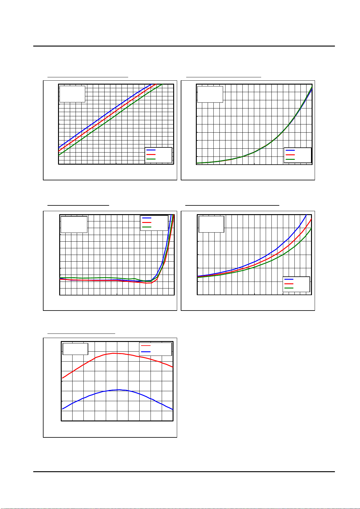
PERFORMANCE DATA
WiMAX OFDM 64QAM signal input. Ta=25degC.
Output Power vs. Input Power Efficiency vs. Output Power
30
Vc=6V
Vref=2.85V
Vcont=0V
25
20
Output Power (dBm)
15
10
-20 -15 -10 -5 0
Input Power (dBm)
2.5GHz
2.6GHz
2.7GHz
20
Vc=6V
18
Vref=2.85V
Vcont=0V
16
14
12
10
8
Efficiency (%)
6
4
2
0
10 15 20 25 30
Output Power (dBm)
EVM vs. Output Power Detector Voltage vs. Output Power
6.0
Vc=6V
5.5
Vref=2.85V
5.0
Vcont=0V
4.5
4.0
3.5
3.0
2.5
EVM (%)
2.0
1.5
1.0
0.5
0.0
10 15 20 25 30
Output Power (dBm)
2.5GHz
2.6GHz
2.7GHz
3.0
Vc=6V
Vref=2.85V
2.5
Vcont=0V
2.0
1.5
Vdet (V)
1.0
0.5
0.0
10 15 20 25 30
Output Power (dBm)
Attenuation Performance
40
Vc=6V
Vref=2.85V
30
20
S21 (dB)
10
0
2.0 2.2 2.4 2.6 2.8 3.0
Frequency (GHz)
Vcont=0V
Vcont=3V
2.5GHz
2.6GHz
2.7GHz
2.5GHz
2.6GHz
2.7GHz
MITSUBISHI ELECTRIC CORP.
(3/7) January-2008
Page 4

MITSUBISHI SEMICONDUCTOR
MGFS36E2527
Specifications are subject to change without notice. 2.5-2.7GHz HBT HYBRID IC
WiMAX OFDM 64QAM signal input.
Output Power vs. Input Power Efficiency vs. Output Power
30
f =2.6GHz
Vc=6V
Vref=2.85V
25
Vcont=0V
20
Output Power (dBm)
15
10
-20 -15 -10 -5 0
Input Power (dBm)
-30degC
0degC
25degC
60degC
85degC
20
f =2.6GHz
18
Vc=6V
Vref=2.85V
16
Vcont=0V
14
12
10
8
Efficiency (%)
6
4
2
0
10 15 20 25 30
Output Power (dBm)
EVM vs. Output Power Detector Voltage vs. Output Power
6.0
f =2.6GHz
5.5
Vc=6V
5.0
Vref=2.85V
4.5
Vcont=0V
4.0
3.5
3.0
2.5
EVM (%)
2.0
1.5
1.0
0.5
0.0
10 15 20 25 30
Output Power (dBm)
-30degC
0degC
25degC
60degC
85degC
3.0
f =2.6GHz
Vc=6V
2.5
Vref=2.85V
Vcont=0V
2.0
1.5
Vdet (V)
1.0
0.5
0.0
10 15 20 25 30
Output Power (dBm)
Attenuation Level
22
f=2.6GHz
Vc=6V
21
Vref=2.85V
20
19
18
Attenuation Level (dB)
17
-30degC
0degC
25degC
60degC
85degC
-30degC
0degC
25degC
60degC
85degC
16
-30 0 30 60 90
Case Temperature (degC)
MITSUBISHI ELECTRIC CORP.
(4/7) January-2008
Page 5

MITSUBISHI SEMICONDUCTOR
MGFS36E2527
Specifications are subject to change without notice. 2.5-2.7GHz HBT HYBRID IC
WiMAX OFDM 64QAM signal input. Ta=25degC.
Output Power vs. Input Power Efficiency vs. Output Power
30
f =2.6GHz
Vc=6V
Vcont=0V
25
20
Output Power (dBm)
15
10
-20 -15 -10 -5 0
Input Power (dBm)
Vref=2.75V
Vref=2.85V
Vref=2.95V
20
f =2.6GHz
18
Vc=6V
Vcont=0V
16
14
12
10
8
Efficiency (%)
6
4
2
0
10 15 20 25 30
Output Power (dBm)
EVM vs. Output Power Detector Voltage vs. Output Power
6.0
f =2.6GHz
5.5
Vc=6V
5.0
Vcont=0V
4.5
4.0
3.5
3.0
2.5
EVM (%)
2.0
1.5
1.0
0.5
0.0
10 15 20 25 30
Output Power (dBm)
Vref=2.75V
Vref=2.85V
Vref=2.95V
3.0
f =2.6GHz
Vc=6V
2.5
Vcont=0V
2.0
1.5
Vdet (V)
1.0
0.5
0.0
10 15 20 25 30
Output Power (dBm)
Attenuation Level
22
f=2.6GHz
Vc=6V
21
20
19
18
Attenuation Level (dB)
17
16
2.7 2.8 2.9 3.0
Reference Voltage (V)
Vref=2.75V
Vref=2.85V
Vref=2.95V
Vref=2.75V
Vref=2.85V
Vref=2.95V
MITSUBISHI ELECTRIC CORP.
(5/7) January-2008
Page 6

MITSUBISHI SEMICONDUCTOR
MGFS36E2527
Specifications are subject to change without notice. 2.5-2.7GHz HBT HYBRID IC
APPLICATION CIRCUIT
Attenuator
Control
RF Input
50ohms
Pin
Vcont
1000pF
Supply
Voltage
PACKAGE OUTLINE
0.3
0.3
2.653.65
1uF
Vcb
Vc1
Vc2
Vc3
1000pF
Vref
GND
Po_det
Pout
Pulse Operation is controlled by Vref
4.5
1stpinmark
1.3(max)
1.0(typ)
4.5
4.1
3.6
1.8
0.5
Reference
1000pF
Voltage
Detector
10nF
50ohms
Dimension in millimeters.
Unless specified tolerance ±0.2mm.
Voltage Out
RF Output
0.5
MITSUBISHI ELECTRIC CORP.
(6/7) January-2008
Page 7

MITSUBISHI SEMICONDUCTOR
MGFS36E2527
Specifications are subject to change without notice. 2.5-2.7GHz HBT HYBRID IC
HANDLING PRECAUTION
1) Work desk, test equipment, soldering iron and worker should be grounded before mounting
and testing. Please note that electric discharge of GaAs HBT is much more sensitive than
that of Si transistor. Handling without ground possibly damages GaAs HBT.
2) The surface of a board on which this product is mounted should be as flat and clean as possible
to prevent a substrate from cracking by bending this product.
3) IR reflow soldering condition is confirmed following profile.
260degC
225degC
(PKG Surface temp.)
≧10sec
≧70sec
180+/-10degC
120+/-20sec
4) Handling precaution at high temperature
This product has the structure of sealing with epoxy resin on grass epoxy substrate. This epoxy resin
gets soft if the temperature exceeds glass transition temperature=120degC, and the thermic
decomposition is occurred if the temperature exceeds 350degC. Therefore, in case of heating this
product, please keep the same heat profile as recommended reflow one.
Please note that crack, flaw or modification may be generated if softened epoxy resin part is handled
with tweezers and etc at high temperature.
5) Cleaning condition
Please select after confirming administrative guidance, legal restrictions, and the mass of the residual
ion contaminant etc., and use it.
6) After soldering, please remove the flux. Please take care that solvent does not penetrate into this
product.
7) GaAs HBT contains As(Arsenic). This product should be dumped as particular industrial waste.
MITSUBISHI ELECTRIC CORP.
(7/7) January-2008
 Loading...