Mitsubishi MGFC5218 Datasheet

PRELIMINARY
Notice : This is not a final specification
Some parametric limits are subject to change.
MITSUBISHI SEMICONDUCTOR <GaAs MMIC>
MGFC5218
K-Band 2-Stage Power Amplifier
DESCRIPTION
The MGFC5218 is a GaAs MMIC chip especially
designed for 18.0 ~ 19.0 GHz band High
Power Amplifier (MPA) .
FEATURES
RF frequency : 18.0 to 19.0 GHz
P1dB : ≥ 29.0 dBm(min.) @ 18.0 to 19.0 GHz
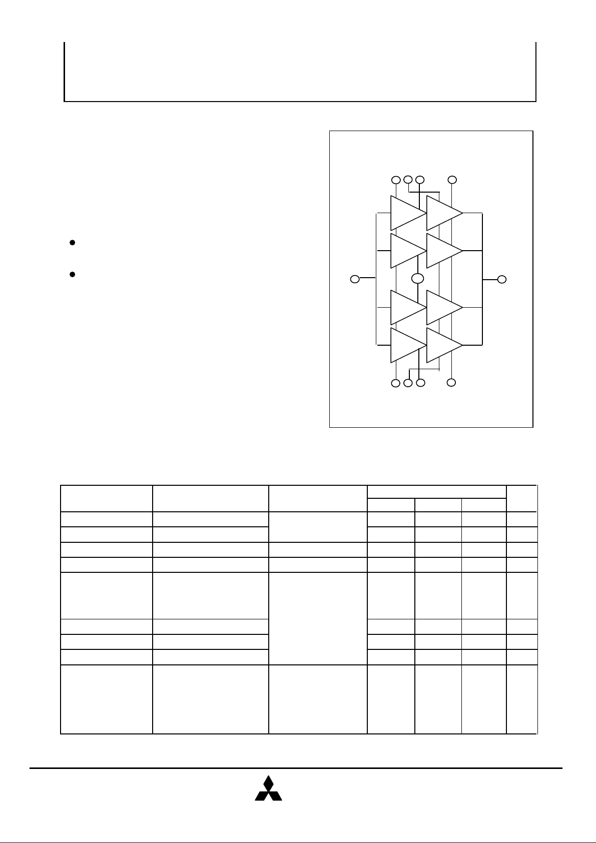
BLOCK DIAGRAM
Vg1
Vg2
Vd1
Vd2
In
Vd1
Vg1
Vg2
Vd1
Vd2
Chip size: 1940 µm x 2000 µm
Out
TARGET SPECIFICATIONS (Ta=25˚C)
Symbol
IDSS1
IDSS2
Vp1
Vp2
P1dB
Gain
Input Return Loss
Output Return Loss
IM3
Drain Saturation Current Vd=3.0V
Drain Saturation Current
Pinch Off Voltage Vd=3.0V,Id=0.6mA
Pinch Off Voltage Vd=3.0V,Id=1.2mA
Output Power at 1 dB
Compression Point
Gain
Input Return Loss
Output Return Loss
Inter Modulation Level
Parameter Test Conditions
f=18 - 20 GHz,
Vd1=Vd2=6.0V ,
Id1=360mA*,
Id2=720mA*
f=18 - 20 GHz,
Vd1=Vd2=6.0V ,
Id1=360mA*,
Id2=720mA*
Pout=TBD
*:Ids at RF off
Limits
Min. Typ. Max. Unit
720
1440
-2.0 -1.0
-2.0 -1.0
29.0
15.0
8.0
8.0
TBD
mA
mA
dBm
dB
dB
dB
dBc
V
V
MITSUBISHI
ELECTRIC
as of July '98

MITSUBISHI SEMICONDUCTOR <GaAs MMIC>
PRELIMINARY
Notice : This is not a final specification
Some parametric limits are subject to change.
K-Band 2-Stage Power Amplifier
DIE SIZE AND BOND PAD LOCATION(UNIT : µM)
MGFC5218
Vg1
(-0.2 to -1.0 V)
RF-in
Vg1
275
Vg2 (-0.2 to -1.0 V)
GND GND
GND
Vg2
130
990
975
1535
Vd1 Vd2
Vd1
Vd1
1940
Vd2
RF-out
GND
MITSUBISHI
ELECTRIC
as of July '98
 Loading...