

PRELIMINARY
Notice : This is not a final specification
Some parametric limits are subject to change.
MITSUBISHI SEMICONDUCTOR <GaAs MMIC>
MGFC5109
Ka-Band 3-Stage Self Bias Low Noise Amplifier
DESCRIPTION
The MGFC5109 is a GaAs MMIC chip
especially designed for 27.0 ~ 30.0 GHz band
Low Noise Amplifier.(LNA) .
FEATURES
RF frequency : 27.0 to 30.0 GHz
Super Low Noise NF=2.5dB (TYP.)
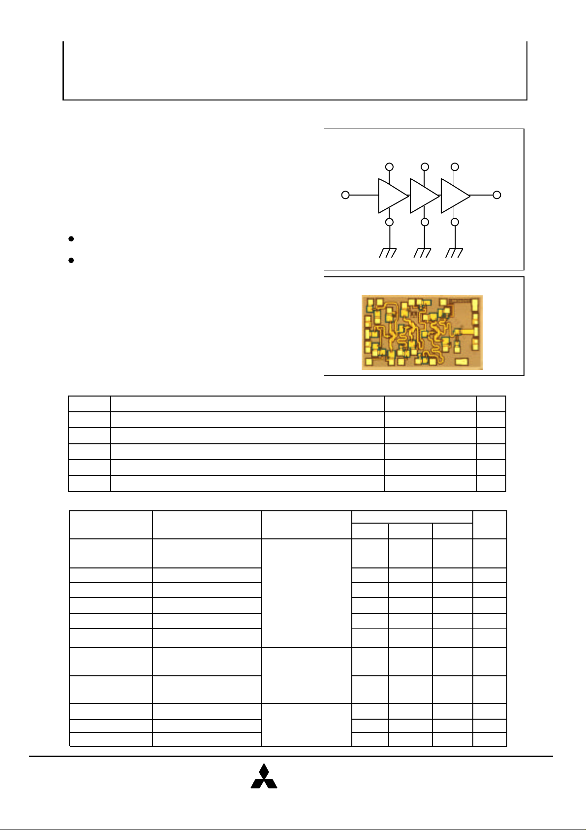
BLOCK DIAGRAM
In
Vg1 Vg3Vg2
PHOTOGRAPH
ABSOLUTE MAXIMUM RATINGS (Ta=25˚C)
Symbol Parameter Values Unit
Vd Drain bias voltage 3 V
Out
Id Drain bias current 30 mA
Vg Gate bias voltage
Pin Maximum peak input power overdrive (Duration < 1sec) TBD dBm
Ta Operating temperature range TBD
-
TARGET SPECIFICATIONS (Ta=25˚C)
Symbol
Fop
Gain
Delta gain
NF
VSWR in Input VSWR
VSWR out
P1dB
Output IP3
Vd
Id Drain bias current mA
Vg
Parameter Test conditions
Operating frequency
range
Small signal gain
Small signal gain flatness
Noise figure
Output VSWR
Output power at 1 dB
compression
Output power at 3rdorder intercept point
Drain bias voltage
Gate bias voltage
Vd=2.5V,Id=20mA
Min.
27.0 30.0
17.0
On-wafer
measurement
Freq=30GHz
Limits
Typ.
18.0
1.5
2.5
2.5:1
2.0:1
(5)
TBD
(17)
TBD
2.5
30
No need
Max.
V
˚C
Unit
GHz
dB
dB
dB
dBm
dBm
V
V
MITSUBISHI
ELECTRIC
as of July '98
MITSUBISHI SEMICONDUCTOR <GaAs MMIC>
PRELIMINARY
Notice : This is not a final specification
Some parametric limits are subject to change.
Ka-Band 3-Stage Self Bias Low Noise Amplifier
DIE SIZE AND BOND PAD LOCATION(UNIT : µm)
1824
1808
1308
808
308
116
MGFC5109
Vd1 Vd2 GNDVd3
GND
RF-in
GND
Vg1 Vg2
145
645
1145
1645
1940
Vg3
GND
RF-out
GND
GND
MITSUBISHI
ELECTRIC
as of July '98
 Loading...