

PRELIMINARY
Notice : This is not a final specification
Some parametric limits are subject to change.
MITSUBISHI SEMICONDUCTOR <GaAs MMIC>
MGFC5108
Ka-Band 3-Stage Self Bias Low Noise Amplifier
DESCRIPTION
The MGFC5108 is a GaAs MMIC chip
especially designed for 24.0 ~ 27.0 GHz band
Low Noise Amplifier.(LNA) .
FEATURES
RF frequency : 24.0 to 27.0 GHz
Super Low Noise NF=2.5dB (TYP.)
Single voltage operation
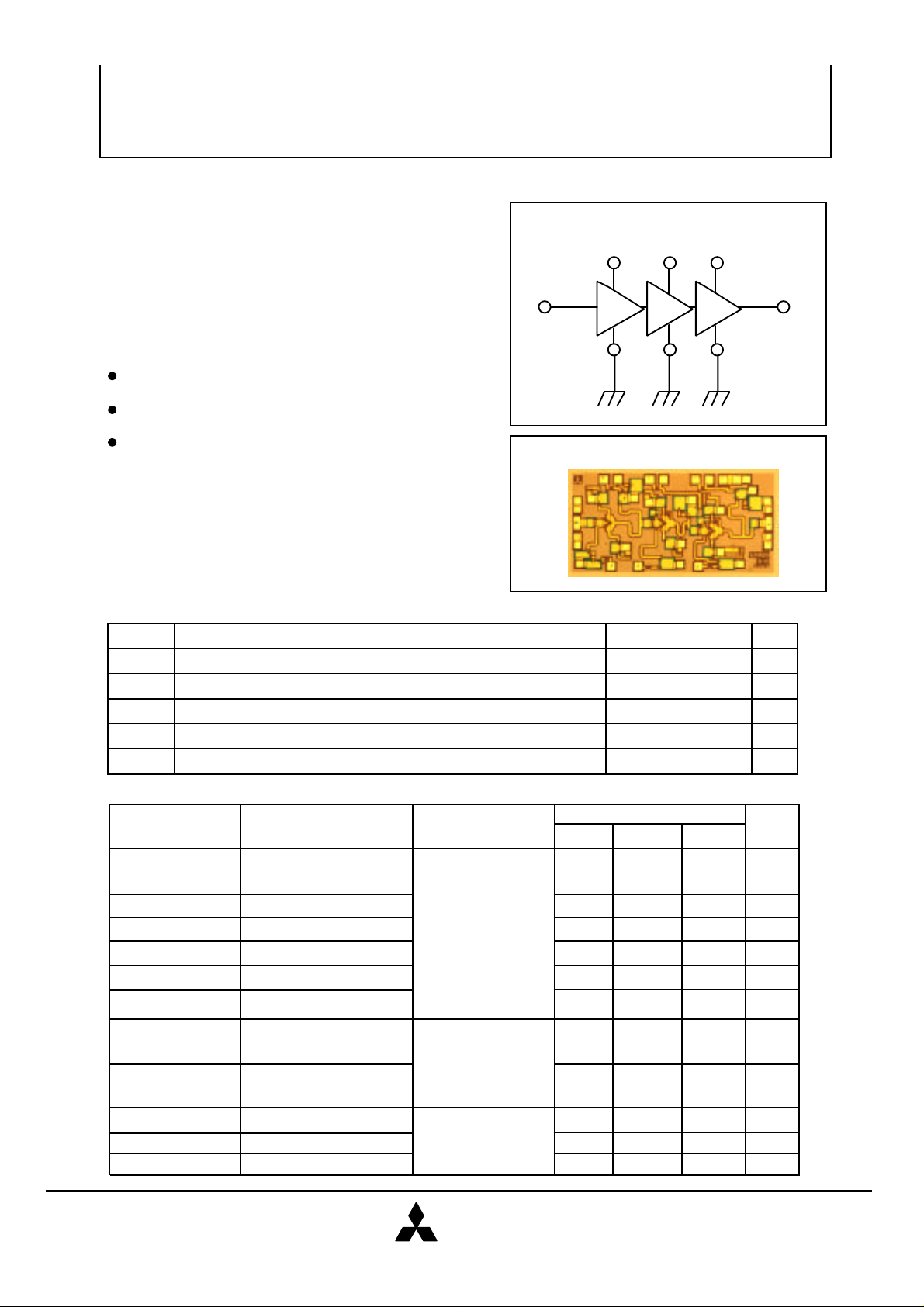
BLOCK DIAGRAM
Vd1 Vd3Vd2
In
Vg1 Vg3Vg2
PHOTOGRAPH
ABSOLUTE MAXIMUM RATINGS (Ta=25˚C)
Symbol Parameter Values Unit
Vd Drain bias voltage 5 V
Out
Id Drain bias current 30 mA
Vg Gate bias voltage
Pin Maximum peak input power overdrive (Duration < 1sec) TBD dBm
Ta Operating temperature range TBD
-
TARGET SPECIFICATIONS (Ta=25˚C)
Symbol
Fop
Gain
Delta gain
NF
VSWR in Input VSWR
VSWR out
P1dB
Output IP3
Vd
Id Drain bias current mA
Vg
Parameter Test conditions
Operating frequency
range
Small signal gain
Small signal gain flatness
Noise figure
Output VSWR
Output power at 1 dB
compression
Output power at 3rdorder intercept point
Drain bias voltage
Gate bias voltage
Vd=5V,Id=30mA
Min.
24.0 27.0
17.0
On-wafer
measurement
Freq=22GHz
Limits
Typ.
18.0
1.5
2.5
(5)
TBD
(17)
TBD
5
30
No need
Max.
2.5:1
2.5:1
V
˚C
Unit
GHz
dB
dB
dB
dBm
dBm
V
V
MITSUBISHI
ELECTRIC
as of July '98
MITSUBISHI SEMICONDUCTOR <GaAs MMIC>
PRELIMINARY
Notice : This is not a final specification
Some parametric limits are subject to change.
Ka-Band 3-Stage Self Bias Low Noise Amplifier
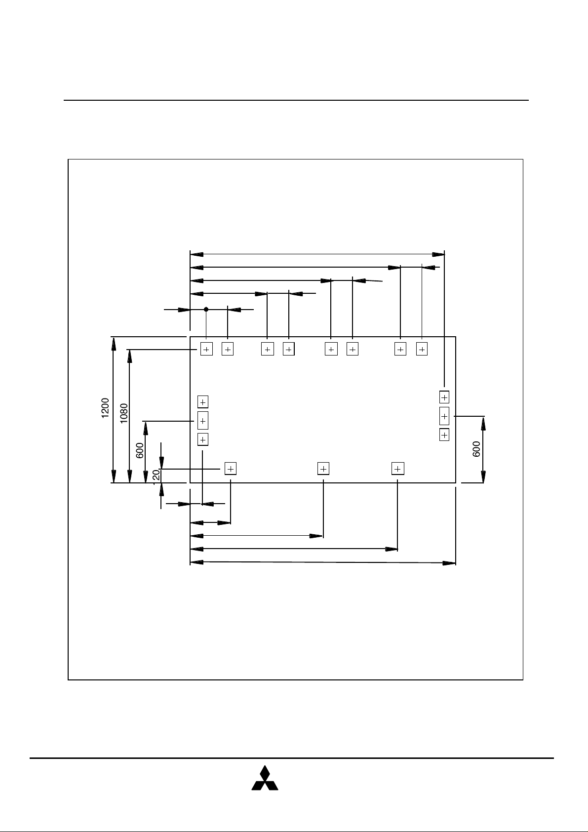
DIE SIZE AND BOND PAD LOCATION(UNIT : µm)
2194
1700
400
150
900
1400
150
150
MGFC5108
150
Vd1a Vd2a GND
Vd1b Vd2b GNDVd3b
GND
RF-in
GND
Vg1 Vg3
106
480
775
1430
Vd3a
Vg2
2300
GND
RF-out
GND
MITSUBISHI
ELECTRIC
as of July '98

PRELIMINARY
Notice : This is not a final specification
Some parametric limits are subject to change.
TYPICAL CHARACTERISTICS
Small Signal Performances
(Vd = 5.0 V, Id = 30 mA, Ta = 25 ˚C )
MITSUBISHI SEMICONDUCTOR <GaAs MMIC>
MGFC5108
Ka-Band 3-Stage Self Bias Low Noise Amplifier
25
20
15
10
5
0
22 23 24 25 26 27 28
VSWR in
VSWR out
Frequency (GHz)
NF
10
8
6
4
2
0
MITSUBISHI
ELECTRIC
as of July '98

PRELIMINARY
Notice : This is not a final specification
Some parametric limits are subject to change.
AN EXAMPLE OF TEST CIRCUIT
5V 5V 5V
Cb Cb Cb
MITSUBISHI SEMICONDUCTOR <GaAs MMIC>
MGFC5108
Ka-Band 3-Stage Self Bias Low Noise Amplifier
:Chip capacitor (39pF)
Cb > 100µF
Vd1a Vd2a
Vd1b Vd2b
GND
RF-in
GND
Vg1 Vg3
*1
*2
*1 Length of bonding wire < 200 µm
*2 Number of bonding wire ≥ 3
Vg2
Vd3a
Vd3b
GND
GND
GND
RF-out
GND
*1
*2
MITSUBISHI
ELECTRIC
as of July '98

PRELIMINARY
Notice : This is not a final specification
Some parametric limits are subject to change.
AN EXAMPLE OF TEST CIRCUIT
2.5V 2.5V 2.5V
MITSUBISHI SEMICONDUCTOR <GaAs MMIC>
MGFC5108
Ka-Band 3-Stage Self Bias Low Noise Amplifier
Cb Cb Cb
Vd1a Vd2a GND
Vd1b Vd2b GNDVd3b
GND
RF-in
GND
Vg1 Vg3
Vd3a
Vg2
*1
*2
:Chip capacitor (39pF)
Cb > 100µF
GND
RF-out
GND
*1
*2
*1 Length of bonding wire < 200 µm
*2 Number of bonding wire ≥ 3
MITSUBISHI
ELECTRIC
as of July '98
 Loading...