

Page 1
Output power at 1dB gain
compression
查询MGFC45V5964A供应商
PRELIMINARY
Notice : This is not a final specification.
Some parametric limits are subject to change.
5.9 - 6.4GHz BAND 32W INTERNALLY MATCHED GaAs FET
DESCRIPTION
The MGFC45V5964A is an internally impedance matched
GaAs power FET especially designed for use in 5.9 - 6.4
GHz band amplifiers. The hermetically sealed metal-ceramic
package guarantees high reliability.
FEATURES
Internally matched to 50 ohm system
High output power
P1dB = 32W (TYP.) @ f=5.9 - 6.4 GHz
High power gain
GLP =9.0 dB (TYP.) @ f=5.9 - 6.4 GHz
High power added efficiency
P.A.E. = 33 % (TYP.) @ f=5.9 - 6.4 GHz
Low Distortion[Item-51]
IM3=-42 dBc(MIN.)@Po=34.5dBm S.C.L.
APPLICATION
5.9 - 6.4 GHz band amplifiers
QUALITY GRADE
IG
RECOMMENDED BIAS CONDITIONS
VDS = 10V
ID = 8 A
Rg=25 ohm Refer to Bias Procedure
ABSOLUTE MAXIMUM RATINGS
27-March'98
MITSUBISHI SEMICONDUCTOR <GaAs FET>
MGFC45V5964A
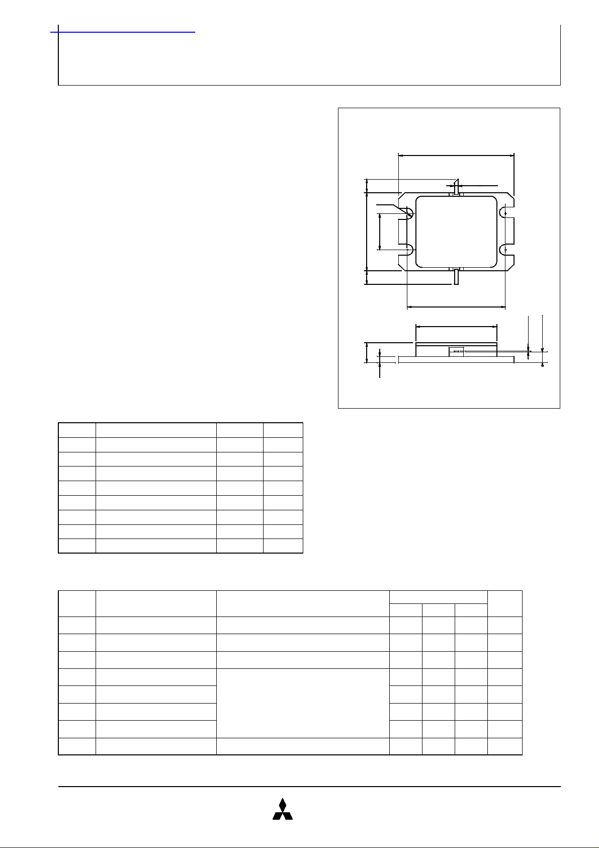
OUTLINE DRAWING Unit:millimeters (inches)
24 +/- 0.3
0.6 +/- 0.15
2MIN
R1.2
8.0 +/- 0.2
17.4 +/- 0.2
2MIN
4.3 +/- 0.4
1.4
GF-38
(1)
20.4 +/- 0.2
16.7
(3)
(1) GATE
(2) SOURCE(FIANGE)
(3) DRAIN
(2)
2.4 +/- 0.2
0.1 +/- 0.05
Symbol Parameter Ratings Unit
VGDO Gate to drain voltage -15 V
VGSO Gate to source voltage -15 V
ID Drain current 30 A
IGR Reverse gate current -60 mA
IGF Forward gate current 126 mA
PT Total power dissipation 125 W
Tch Channel temperature 175 deg.C
Tstg Storage temperature -65/+175 deg.C
*1 : Tc=25 Deg.C
ABSOLUTE MAXIMUM RATINGS
Symbol Parameter Test conditions
IDSS Saturated drain current VDS = 3V , VGS = 0V - 24 - A
Gm Transconductance VDS = 3V , ID = 8A - 8 - S
VGS(off) Gate to source cut-off voltage VDS = 3V , ID = 160mA - - -5 V
P1dB
GLP Linear power gain VDS = 10V , ID = 8A , f = 5.9 - 6.4 GHz 8 9 - dB
PAE Power added efficiency - 33 - %
44.5 45 - dBm
Limits
Min Typ Max
Unit
IM3 3rd order IM distortion -42 -45 - dBc
Rth(ch-c) Thermal resistance *1 Delta Vf method - ‑ 1.0 Deg.C/W
*1 : Channel to case
*2 : Item-51,2tone test,Po=34.5dBm Single Carrier Level,f=6.4GHz, Delta f=10MHz
MITSUBISHI
ELECTRIC
Page 2
27-March'98
5.9 - 6.4 GHz BAND 32W INTERNALLY MATCHED GaAs FET
11S21S12S22
PRELIMINARY
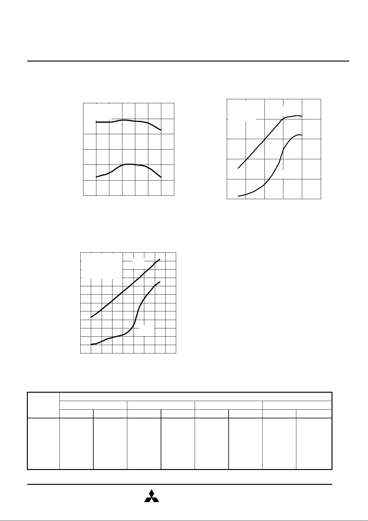
LINEAR POWER GAIN GLP(dB)
OUTPUT POWER Po (dBm S.C.L.)
OUTPUT POWER Po(dBm)
Notice : This is not a final specification.
Some parametric limits are subject to change.
TYPICAL CHARACTERISTICS (Ta=25 Deg.C)
MITSUBISHI SEMICONDUCTOR <GaAs FET>
MGFC45V5964A
P1dB ,GLP vs. f
47
VDS=10(V)
IDS=8(A)
P1dB
46
45
44
OUTPUT POWER P1dB (dBm)
43
GLP
42
41
5.8 5.9 6.0 6.1 6.2 6.3 6.4 6.5
FERQUENCY (GHz)
Po IM3 vs. Pin
44
VDS=10(V)
42
IDS=8(A)
f=6.4(GHz)
40
Delta f=10(MHz)
38
Po
36
34
32
30
28
26
IM3
24
22
20
18 20 22 24 26 28 30 32 34 36
INPUT POWER Pin(dBm S.C.L.)
14
13
12
11
10
9
8
0
-10
-20
-30
-40
-50
-60
IM3(dBc)
Po , PAE vs. Pin
50
VDS=10(V)
IDS=8(A)
f=6.15(GHz)
45
40
35
30
25
20 25 30 35 40 45
INPUTPOWER Pin(dBm)
Po
PAE
50
40
30
20
10
POWER ADDED EFFICIECY PAE (%)
0
S PARAMETERS (Ta=25 Deg.C , V
=10V , IDS=8A)
DS
S Parameters (TYP.)
f
S
(GHz) Magn. Angle(deg.) Magn. Angle(deg.) Magn. Angle(deg.) Magn. Angle(deg.)
5.90 0.61 159 2.957 -44 0.04 -117 0.21 160
6.00 0.55 138 3.071 -62 0.05 -134 0.22 134
6.10 0.48 115 3.119 -81 0.06 -152 0.25 112
6.20 0.41 92 3.148 -100 0.07 -167 0.26 91
6.30 0.34 65 3.143 -118 0.08 175 0.26 73
6.40 0.28 36 3.122 -137 0.09 160 0.25 55
MITSUBISHI
ELECTRIC
 Loading...